DM74LS169A Synchronous 4-Bit Up/Down Binary Counter
|
|
|
- Dwain O’Connor’
- 9 years ago
- Views:
Transcription
1 Synchronous 4-Bit Up/Down Binary Counter General Description This synchronous presettable counter features an internal carry look-ahead for cascading in high-speed counting applications. Synchronous operation is provided by having all flip-flops clocked simultaneously, so that the outputs all change at the same time when so instructed by the countenable inputs and internal gating. This mode of operation helps eliminate the output counting spikes that are normally associated with asynchronous (ripple clock) counters. A buffered clock input triggers the four masterslave flip-flops on the rising edge of the clock waveform. This counter is fully programmable; that is, the outputs may each be preset either HIGH or LOW. The load input circuitry allows loading with the carry-enable output of cascaded counters. As loading is synchronous, setting up a low level at the load input disables the counter and causes the outputs to agree with the data inputs after the next clock pulse. The carry look-ahead circuitry permits cascading counters for n-bit synchronous applications without additional gating. Both count-enable inputs (P and T) must be LOW to count. The direction of the count is determined by the level of the UP/DOWN input. When the input is HIGH, the counter counts UP; when LOW, it counts DOWN. Input T is fed forward to enable the carry outputs. The carry output thus August 1986 Revised April 2000 enabled will produce a low-level output pulse with a duration approximately equal to the high portion of the Q A output when counting UP, and approximately equal to the low portion of the Q A output when counting DOWN. This lowlevel overflow carry pulse can be used to enable successively cascaded stages. Transitions at the enable P or T inputs are allowed regardless of the level of the clock input. All inputs are diode clamped to minimize transmission-line effects, thereby simplifying system design. This counter features a fully independent clock circuit. Changes at control inputs (enable P, enable T, load, UP/ DOWN), which modify the operating mode, have no effect until clocking occurs. The function of the counter (whether enabled, disabled, loading, or counting) will be dictated solely by the conditions meeting the stable setup and hold times. Features Fully synchronous operation for counting and programming. Internal look-ahead for fast counting. Carry output for n-bit cascading. Fully independent clock circuit DM74LS169A Synchronous 4-Bit Up/Down Binary Counter Ordering Code: Order Number Package Number Package Description DM74LS169AM M16A 16-Lead Small Outline Integrated Circuit (SOIC), JEDEC MS-012, Narrow DM74LS169AN N16E 16-Lead Plastic Dual-In-Line Package (PDIP), JEDEC MS-001, Wide Devices also available in Tape and Reel. Specify by appending the suffix letter X to the ordering code. Connection Diagram 2000 Fairchild Semiconductor Corporation DS

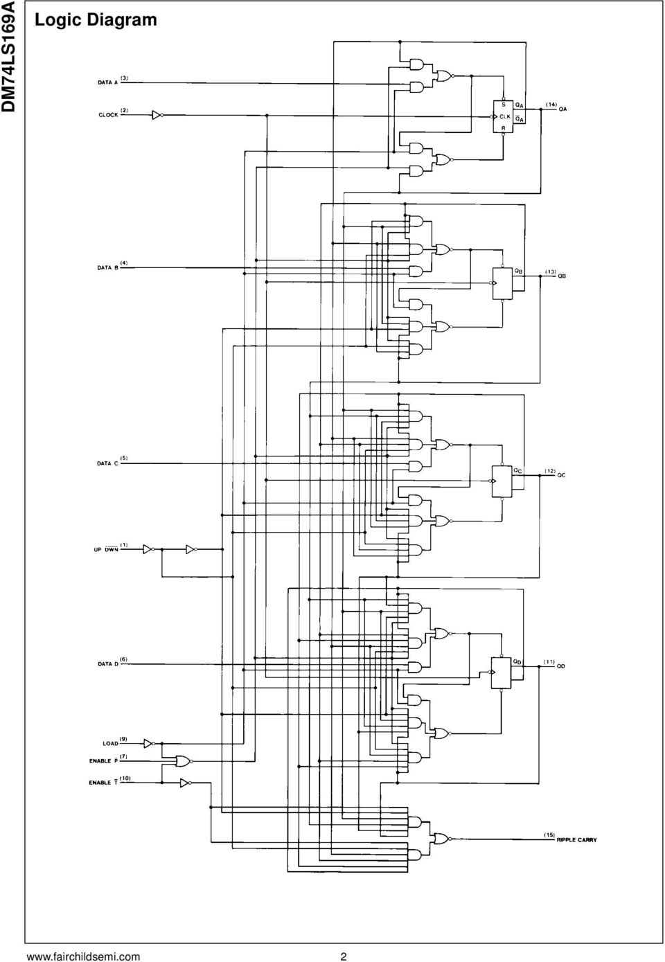
2 Logic Diagram 2
3 Timing Diagram DM74LS169A Typical Load, Count, and Inhibit Sequences 3

4 Absolute Maximum Ratings(Note 1) Supply Voltage 7V Input Voltage 7V Operating Free Air Temperature Range 0 C to +70 C Storage Temperature Range 65 C to +150 C Note 1: The Absolute Maximum Ratings are those values beyond which the safety of the device cannot be guaranteed. The device should not be operated at these limits. The parametric values defined in the Electrical Characteristics tables are not guaranteed at the absolute maximum ratings. The Recommended Operating Conditions table will define the conditions for actual device operation. Recommended Operating Conditions Symbol Parameter Min Nom Max Units V CC Supply Voltage V V IH HIGH Level Input Voltage 2 V V IL LOW Level Input Voltage 0.8 V I OH HIGH Level Output Current 0.4 ma I OL LOW Level Output Current 8 ma f CLK Clock Frequency (Note 2) 0 25 MHz Clock Frequency (Note 3) 0 20 MHz t W Clock Pulse Width (Note 4) 25 ns t SU Setup Time Data 20 (Note 4) Enable 20 T or P ns Load 25 U/D 30 t H Hold Time (Note 4) 0 ns T A Free Air Operating Temperature 0 70 C Note 2: C L = 15 pf, R L = 2 kω, T A = 25 C and V CC = 5V. Note 3: C L = 50 pf, R L = 2 kω, T A = 25 C and V CC = 5V. Note 4: T A = 25 C and V CC = 5V. Electrical Characteristics over recommended operating free air temperature range (unless otherwise noted) Typ Symbol Parameter Conditions Min (Note 5) Max Units V I Input Clamp Voltage V CC = Min, I I = 18 ma 1.5 V V OH HIGH Level V CC = Min, I OH = Max Output Voltage V IL = Max, V IH = Min V V OL LOW Level V CC = Min, I OL = Max Output Voltage V IL = Max, V IH = Min V I OL = 4 ma, V CC = Min I I Input Max V CC = Max Enable T 0.2 Input Voltage V I = 7V Others 0.1 ma I IH HIGH Level V CC = Max Enable T 40 Input Current V I = 2.7V Others 20 µa I IL LOW Level V CC = Max Enable T 0.8 Input Current V I = 0.4V Others 0.4 ma I OS Short Circuit Output Current V CC = Max (Note 6) ma I CC Supply Current V CC = Max (Note 7) ma Note 5: All typicals are at V CC = 5V and T A = 25 C. Note 6: Not more than one output should be shorted at a time, and the duration should not exceed one second. Note 7: I CC is measured after a momentary 4.5V, then ground, is applied to the CLOCK with all other inputs grounded and all the outputs OPEN. 4

5 Switching Characteristic at V CC = 5V and T A = 25 C From (Input) R L = 2 kω Symbol Parameter To (Output) C L = 15 pf C L = 50 pf Units Min Max Min Max f MAX Maximum Clock Frequency MHz t PLH Propagation Delay Time Clock to LOW-to-HIGH Level Output ns t PHL Propagation Delay Time Clock to HIGH-to-LOW Level Output ns t PLH Propagation Delay Time Clock to LOW-to-HIGH Level Output Any Q ns t PHL Propagation Delay Time Clock to HIGH-to-LOW Level Output Any Q ns t PLH Propagation Delay Time Enable T to LOW-to-HIGH Level Output ns t PHL Propagation Delay Time Enable T to HIGH-to-LOW Level Output ns t PLH Propagation Delay Time Up/Down to LOW-to-HIGH Level Output (Note 8) ns t PHL Propagation Delay Time Up/Down to HIGH-to-LOW Level Output (Note 8) ns Note 8: The propagation delay from UP/DOWN to RIPPLE CARRY must be measured with the counter at either a minimum or a maximum count. As the logic level of the UP/DOWN input is changed, the ripple carry output will follow. If the count is minimum, the RIPPLE CARRY output transition will be in phase. If the count is maximum, the RIPPLE CARRY output will be out of phase. DM74LS169A 5
 25 30 ns t PHL Propagation Delay Time Up/Down to HIGH-to-LOW Level Output")
6 Physical Dimensions inches (millimeters) unless otherwise noted 16-Lead Small Outline Integrated Circuit (SOIC), JEDEC MS-012, Narrow Package Number M16A 6

7 Physical Dimensions inches (millimeters) unless otherwise noted (Continued) 16-Lead Plastic Dual-In-Line Package (PDIP), JEDEC MS-001, Wide Package Number N16E DM74LS169A Synchronous 4-Bit Up/Down Binary Counter Fairchild does not assume any responsibility for use of any circuitry described, no circuit patent licenses are implied and Fairchild reserves the right at any time without notice to change said circuitry and specifications. LIFE SUPPORT POLICY FAIRCHILD S PRODUCTS ARE NOT AUTHORIZED FOR USE AS CRITICAL COMPONENTS IN LIFE SUPPORT DEVICES OR SYSTEMS WITHOUT THE EXPRESS WRITTEN APPROVAL OF THE PRESIDENT OF FAIRCHILD SEMICONDUCTOR CORPORATION. As used herein: 1. Life support devices or systems are devices or systems which, (a) are intended for surgical implant into the body, or (b) support or sustain life, and (c) whose failure to perform when properly used in accordance with instructions for use provided in the labeling, can be reasonably expected to result in a significant injury to the user. 2. A critical component in any component of a life support device or system whose failure to perform can be reasonably expected to cause the failure of the life support device or system, or to affect its safety or effectiveness

1-800-831-4242
 Distributed by: www.jameco.com 1-800-831-4242 The content and copyrights of the attached material are the property of its owner. DM74LS161A DM74LS163A Synchronous 4-Bit Binary Counters General Description
DM74LS191 Synchronous 4-Bit Up/Down Counter with Mode Control
 August 1986 Revised February 1999 DM74LS191 Synchronous 4-Bit Up/Down Counter with Mode Control General Description The DM74LS191 circuit is a synchronous, reversible, up/ down counter. Synchronous operation
DM74LS193 Synchronous 4-Bit Binary Counter with Dual Clock
 September 1986 Revised March 2000 DM74LS193 Synchronous 4-Bit Binary Counter with Dual Clock General Description The DM74LS193 circuit is a synchronous up/down 4-bit binary counter. Synchronous operation
54LS169 DM54LS169A DM74LS169A Synchronous 4-Bit Up Down Binary Counter
 54LS169 DM54LS169A DM74LS169A Synchronous 4-Bit Up Down Binary Counter General Description This synchronous presettable counter features an internal carry look-ahead for cascading in high-speed counting
DM74LS112A Dual Negative-Edge-Triggered Master-Slave J-K Flip-Flop with Preset, Clear, and Complementary Outputs
 August 1986 Revised March 2000 DM74LS112A Dual Negative-Edge-Triggered Master-Slave J-K Flip-Flop with Preset, Clear, and Complementary General Description This device contains two independent negative-edge-triggered
DM7474 Dual Positive-Edge-Triggered D-Type Flip-Flops with Preset, Clear and Complementary Outputs
 DM7474 Dual Positive-Edge-Triggered D-Type Flip-Flops with Preset, Clear and Complementary Outputs General Description This device contains two independent positive-edge-triggered D-type flip-flops with
74LS193 Synchronous 4-Bit Binary Counter with Dual Clock
 74LS193 Synchronous 4-Bit Binary Counter with Dual Clock General Description The DM74LS193 circuit is a synchronous up/down 4-bit binary counter. Synchronous operation is provided by having all flip-flops
DM74LS00 Quad 2-Input NAND Gate
 DM74LS00 Quad 2-Input NAND Gate General Description This device contains four independent gates each of which performs the logic NAND function. Ordering Code: August 1986 Revised March 2000 Order Number
DM74LS05 Hex Inverters with Open-Collector Outputs
 Hex Inverters with Open-Collector Outputs General Description This device contains six independent gates each of which performs the logic INVERT function. The open-collector outputs require external pull-up
DM54161 DM74161 DM74163 Synchronous 4-Bit Counters
 DM54161 DM74161 DM74163 Synchronous 4-Bit Counters General Description These synchronous presettable counters feature an internal carry look-ahead for application in high-speed counting designs The 161
54191 DM54191 DM74191 Synchronous Up Down 4-Bit Binary Counter with Mode Control
 54191 DM54191 DM74191 Synchronous Up Down 4-Bit Binary Counter with Mode Control General Description This circuit is a synchronous reversible up down counter The 191 is a 4-bit binary counter Synchronous
CD4027BC Dual J-K Master/Slave Flip-Flop with Set and Reset
 October 1987 Revised March 2002 CD4027BC Dual J-K Master/Slave Flip-Flop with Set and Reset General Description The CD4027BC dual J-K flip-flops are monolithic complementary MOS (CMOS) integrated circuits
DM74LS157 DM74LS158 Quad 2-Line to 1-Line Data Selectors/Multiplexers
 September 1986 Revised April 2000 DM74LS157 DM74LS158 Quad 2-Line to 1-Line Data Selectors/Multiplexers General Description These data selectors/multiplexers contain inverters and drivers to supply full
DM74LS151 1-of-8 Line Data Selector/Multiplexer
 1-of-8 Line Data Selector/Multiplexer General Description This data selector/multiplexer contains full on-chip decoding to select the desired data source. The DM74LS151 selects one-of-eight data sources.
DM74LS153 Dual 1-of-4 Line Data Selectors/Multiplexers
 Dual 1-of-4 Line Data Selectors/Multiplexers General Description Each of these data selectors/multiplexers contains inverters and drivers to supply fully complementary, on-chip, binary decoding data selection
74AC191 Up/Down Counter with Preset and Ripple Clock
 74AC191 Up/Down Counter with Preset and Ripple Clock General Description The AC191 is a reversible modulo 16 binary counter. It features synchronous counting and asynchronous presetting. The preset feature
CD40174BC CD40175BC Hex D-Type Flip-Flop Quad D-Type Flip-Flop
 Hex D-Type Flip-Flop Quad D-Type Flip-Flop General Description The CD40174BC consists of six positive-edge triggered D- type flip-flops; the true outputs from each flip-flop are externally available. The
74F74 Dual D-Type Positive Edge-Triggered Flip-Flop
 Dual D-Type Positive Edge-Triggered Flip-Flop General Description The F74 is a dual D-type flip-flop with Direct Clear and Set inputs and complementary (Q, Q) outputs. Information at the input is traferred
MM74HC174 Hex D-Type Flip-Flops with Clear
 Hex D-Type Flip-Flops with Clear General Description The MM74HC174 edge triggered flip-flops utilize advanced silicon-gate CMOS technology to implement D-type flipflops. They possess high noise immunity,
DM74LS47 BCD to 7-Segment Decoder/Driver with Open-Collector Outputs
 DM74LS47 BCD to 7-Segment Decoder/Driver with Open-Collector Outputs General Description The DM74LS47 accepts four lines of BCD (8421) input data, generates their complements internally and decodes the
MM74HC273 Octal D-Type Flip-Flops with Clear
 MM74HC273 Octal D-Type Flip-Flops with Clear General Description The MM74HC273 edge triggered flip-flops utilize advanced silicon-gate CMOS technology to implement D-type flipflops. They possess high noise
54LS193 DM54LS193 DM74LS193 Synchronous 4-Bit Up Down Binary Counters with Dual Clock
 54LS193 DM54LS193 DM74LS193 Synchronous 4-Bit Up Down Binary Counters with Dual Clock General Description This circuit is a synchronous up down 4-bit binary counter Synchronous operation is provided by
DM9368 7-Segment Decoder/Driver/Latch with Constant Current Source Outputs
 DM9368 7-Segment Decoder/Driver/Latch with Constant Current Source Outputs General Description The DM9368 is a 7-segment decoder driver incorporating input latches and constant current output circuits
CD4001BC/CD4011BC Quad 2-Input NOR Buffered B Series Gate Quad 2-Input NAND Buffered B Series Gate
 CD4001BC/CD4011BC Quad 2-Input NOR Buffered B Series Gate Quad 2-Input NAND Buffered B Series Gate General Description The CD4001BC and CD4011BC quad gates are monolithic complementary MOS (CMOS) integrated
CD4013BC Dual D-Type Flip-Flop
 CD4013BC Dual D-Type Flip-Flop General Description The CD4013B dual D-type flip-flop is a monolithic complementary MOS (CMOS) integrated circuit constructed with N- and P-channel enhancement mode transistors.
74F675A 16-Bit Serial-In, Serial/Parallel-Out Shift Register
 74F675A 16-Bit Serial-In, Serial/Parallel-Out Shift Register General Description The 74F675A contai a 16-bit serial in/serial out shift register and a 16-bit parallel out storage register. Separate serial
74AC139 74ACT139 Dual 1-of-4 Decoder/Demultiplexer
 Dual 1-of-4 Decoder/Demultiplexer General Description The AC/ACT139 is a high-speed, dual 1-of-4 decoder/ demultiplexer. The device has two independent decoders, each accepting two inputs and providing
MM74HC4538 Dual Retriggerable Monostable Multivibrator
 MM74HC4538 Dual Retriggerable Monostable Multivibrator General Description The MM74HC4538 high speed monostable multivibrator (one shots) is implemented in advanced silicon-gate CMOS technology. They feature
5495A DM7495 4-Bit Parallel Access Shift Registers
 5495A DM7495 4-Bit Parallel Access Shift Registers General Description These 4-bit registers feature parallel and serial inputs parallel outputs mode control and two clock inputs The registers have three
MM74HCT373 MM74HCT374 3-STATE Octal D-Type Latch 3-STATE Octal D-Type Flip-Flop
 3-STATE Octal D-Type Latch 3-STATE Octal D-Type Flip-Flop General Description The MM74HCT373 octal D-type latches and MM74HCT374 Octal D-type flip flops advanced silicongate CMOS technology, which provides
CD4001BC/CD4011BC Quad 2-Input NOR Buffered B Series Gate Quad 2-Input NAND Buffered B Series Gate
 Quad 2-Input NOR Buffered B Series Gate Quad 2-Input NAND Buffered B Series Gate General Description The CD4001BC and CD4011BC quad gates are monolithic complementary MOS (CMOS) integrated circuits cotructed
CD4043BC CD4044BC Quad 3-STATE NOR R/S Latches Quad 3-STATE NAND R/S Latches
 CD4043BC CD4044BC Quad 3-STATE NOR R/S Latches Quad 3-STATE NAND R/S Latches General Description The CD4043BC are quad cross-couple 3-STATE CMOS NOR latches, and the CD4044BC are quad cross-couple 3- STATE
CD4013BC Dual D-Type Flip-Flop
 Dual D-Type Flip-Flop General Description The CD4013B dual D-type flip-flop is a monolithic complementary MOS (CMOS) integrated circuit cotructed with N- and P-channel enhancement mode traistors. Each
DM74121 One-Shot with Clear and Complementary Outputs
 June 1989 Revised July 2001 DM74121 One-Shot with Clear and Complementary Outputs General Description The DM74121 is a monostable multivibrator featuring both positive and negative edge triggering with
MM74HC14 Hex Inverting Schmitt Trigger
 MM74HC14 Hex Inverting Schmitt Trigger General Description The MM74HC14 utilizes advanced silicon-gate CMOS technology to achieve the low power dissipation and high noise immunity of standard CMOS, as
DM74157 Quad 2-Line to 1-Line Data Selectors/Multiplexers
 DM74157 Quad 2-Line to 1-Line Data Selectors/Multiplexers General Description These data selectors/multiplexers contain inverters and drivers to supply full on-chip data selection to the four out-put gates.
MM74C74 Dual D-Type Flip-Flop
 Dual D-Type Flip-Flop General Description The MM74C74 dual D-type flip-flop is a monolithic complementary MOS (CMOS) integrated circuit cotructed with N- and P-channel enhancement traistors. Each flip-flop
74AC138 74ACT138 1-of-8 Decoder/Demultiplexer
 1-of-8 Decoder/Demultiplexer General Description The AC/ACT138 is a high-speed 1-of-8 decoder/demultiplexer. This device is ideally suited for high-speed bipolar memory chip select address decoding. The
DM74LS373/DM74LS374 3-STATE Octal D-Type Transparent Latches and Edge-Triggered Flip-Flops
 DM74LS373/DM74LS374 3-STATE Octal D-Type Transparent Latches and Edge-Triggered Flip-Flops General Description These 8-bit registers feature totem-pole 3-STATE outputs designed specifically for driving
5485 DM5485 DM7485 4-Bit Magnitude Comparators
 5485 DM5485 DM7485 4-Bit Magnitude Comparators General Description These 4-bit magnitude comparators perform comparison of straight binary or BCD codes Three fully-decoded decisions about two 4-bit words
74VHC574 Octal D-Type Flip-Flop with 3-STATE Outputs
 74HC574 Octal D-Type Flip-Flop with 3-STATE Outputs General Description Ordering Code: March 1993 Revised May 2005 The HC574 is an advanced high speed CMOS octal flipflop with 3-STATE output fabricated
74F168*, 74F169 4-bit up/down binary synchronous counter
 INTEGRATED CIRCUITS 74F168*, * Discontinued part. Please see the Discontinued Product List in Section 1, page 21. 1996 Jan 5 IC15 Data Handbook FEATURES Synchronous counting and loading Up/Down counting
54157 DM54157 DM74157 Quad 2-Line to 1-Line Data Selectors Multiplexers
 54157 DM54157 DM74157 Quad 2-Line to 1-Line Data Selectors Multiplexers General Description These data selectors multiplexers contain inverters and drivers to supply full on-chip data selection to the
MM74C150 MM82C19 16-Line to 1-Line Multiplexer 3-STATE 16-Line to 1-Line Multiplexer
 MM74C150 MM82C19 16-Line to 1-Line Multiplexer 3-STATE 16-Line to 1-Line Multiplexer General Description The MM74C150 and MM82C19 multiplex 16 digital lines to 1 output. A 4-bit address code determines
Obsolete Product(s) - Obsolete Product(s)
 - Obsolete Product(s)") SYNCHRONOUS PROGRAMMABLE 4-BIT BINARY COUNTER WITH ASYNCHRONOUS CLEAR INTERNAL LOOK-AHEAD FOR FAST COUNTING CARRY OUTPUT FOR CASCADING SYNCHRONOUSLY PROGRAMMABLE LOW-POWER TTL COMPATIBILITY STANDARDIZED
SYNCHRONOUS PROGRAMMABLE 4-BIT BINARY COUNTER WITH ASYNCHRONOUS CLEAR INTERNAL LOOK-AHEAD FOR FAST COUNTING CARRY OUTPUT FOR CASCADING SYNCHRONOUSLY PROGRAMMABLE LOW-POWER TTL COMPATIBILITY STANDARDIZED
Quad 2-Line to 1-Line Data Selectors Multiplexers
 54LS157 DM54LS157 DM74LS157 54LS158 DM54LS158 DM74LS158 Quad 2-Line to 1-Line Data Selectors Multiplexers General Description These data selectors multiplexers contain inverters and drivers to supply full
CD4040BC, 12-Stage Ripple Carry Binary Counters CD4060BC, 14-Stage Ripple Carry Binary Counters
 CD4040BC, 12-Stage Ripple Carry Binary Counters CD4060BC, 14-Stage Ripple Carry Binary Counters Features Wide supply voltage range: 3.0V to 15V High noise immunity: 0.45 V DD (Typ.) Low power TTL compatibility:
MM74C150 MM82C19 16-Line to 1-Line Multiplexer 3-STATE 16-Line to 1-Line Multiplexer
 MM74C150 MM82C19 16-Line to 1-Line Multiplexer 3-STATE 16-Line to 1-Line Multiplexer General Description The MM74C150 and MM82C19 multiplex 16 digital lines to 1 output. A 4-bit address code determines
DM54LS260 DM74LS260 Dual 5-Input NOR Gate
 DM54LS260 DM74LS260 Dual 5-Input NOR Gate General Description This device contains two individual five input gates each of which perform the logic NOR function Connection Diagram Dual-In-Line Package TL
CD4027BM CD4027BC Dual J-K Master Slave Flip-Flop with Set and Reset
 CD4027BM CD4027BC Dual J-K Master Slave Flip-Flop with Set and Reset General Description These dual J-K flip-flops are monolithic complementary MOS (CMOS) integrated circuits constructed with N- and P-
DM74184 DM74185A BCD-to-Binary and Binary-to-BCD Converters
 DM74184 DM74185A BCD-to-Binary and Binary-to-BCD Converters General Description These monolithic converters are derived from the 256-bit read only memories DM5488 and DM7488 Emitter connections are made
SN54HC191, SN74HC191 4-BIT SYNCHRONOUS UP/DOWN BINARY COUNTERS
 Single Down/Up Count-Control Line Look-Ahead Circuitry Enhances Speed of Cascaded Counters Fully Synchronous in Count Modes Asynchronously Presettable With Load Control Package Options Include Plastic
CD4008BM CD4008BC 4-Bit Full Adder
 CD4008BM CD4008BC 4-Bit Full Adder General Description The CD4008B types consist of four full-adder stages with fast look-ahead carry provision from stage to stage Circuitry is included to provide a fast
NOTE: The Flatpak version has the same pinouts (Connection Diagram) as the Dual In-Line Package.
 as the Dual In-Line Package.") PRESETTABLE BCD/DECADE UP/DOWN COUNTERS PRESETTABLE 4-BIT BINARY UP/DOWN COUNTERS The SN54/74LS90 is a synchronous UP/DOWN BCD Decade (842) Counter and the SN54/74LS9 is a synchronous UP/DOWN Modulo-6
PRESETTABLE BCD/DECADE UP/DOWN COUNTERS PRESETTABLE 4-BIT BINARY UP/DOWN COUNTERS The SN54/74LS90 is a synchronous UP/DOWN BCD Decade (842) Counter and the SN54/74LS9 is a synchronous UP/DOWN Modulo-6
INTEGRATED CIRCUITS. For a complete data sheet, please also download:
 INTEGRATED CIRCUITS DATA SEET For a complete data sheet, please also download: The IC6 74C/CT/CU/CMOS ogic Family Specifications The IC6 74C/CT/CU/CMOS ogic Package Information The IC6 74C/CT/CU/CMOS ogic
NOTE: The Flatpak version has the same pinouts (Connection Diagram) as the Dual In-Line Package.
 as the Dual In-Line Package.") PRESETTABLE BCD/DECADE UP/DOWN COUNTERS PRESETTABLE 4-BIT BINARY UP/DOWN COUNTERS The SN54/74LS190 is a synchronous UP/DOWN BCD Decade (8421) Counter and the SN54/74LS191 is a synchronous UP/DOWN Modulo-
PRESETTABLE BCD/DECADE UP/DOWN COUNTERS PRESETTABLE 4-BIT BINARY UP/DOWN COUNTERS The SN54/74LS190 is a synchronous UP/DOWN BCD Decade (8421) Counter and the SN54/74LS191 is a synchronous UP/DOWN Modulo-
74VHC112 Dual J-K Flip-Flops with Preset and Clear
 74VHC112 Dual J-K Flip-Flops with Preset and Clear Features High speed: f MAX = 200MHz (Typ.) at V CC = 5.0V Low power dissipation: I CC = 2µA (Max.) at T A = 25 C High noise immunity: V NIH = V NIL =
SN54ALS191A, SN74ALS191A SYNCHRONOUS 4-BIT UP/DOWN BINARY COUNTERS
 Single own/ Up Count-Control Line Look-Ahead Circuitry Enhances Speed of Cascaded Counters Fully Synchronous in Count Modes Asynchronously Presettable With Load Control Package Optio Include Plastic Small-Outline
MC14008B. 4-Bit Full Adder
 4-Bit Full Adder The MC4008B 4bit full adder is constructed with MOS PChannel and NChannel enhancement mode devices in a single monolithic structure. This device consists of four full adders with fast
54LS174,54LS175,DM54LS174,DM54LS175, DM74LS174,DM74LS175
 54LS174,54LS175,DM54LS174,DM54LS175, DM74LS174,DM74LS175 54LS174 DM54LS174 DM74LS174 54LS175 DM54LS175 DM74LS175 Hex/Quad D Flip-Flops with Clear Literature Number: SNOS290A 54LS174 DM54LS174 DM74LS174
HEF4021B. 1. General description. 2. Features and benefits. 3. Ordering information. 8-bit static shift register
 Rev. 10 21 March 2016 Product data sheet 1. General description 2. Features and benefits 3. Ordering information The is an (parallel-to-serial converter) with a synchronous serial data input (DS), a clock
SN54/74LS192 SN54/74LS193
 PRESEABLE BCD/DECADE UP/DOWN COUNER PRESEABLE 4-BI BINARY UP/DOWN COUNER he SN4/74LS2 is an UP/DOWN BCD Decade (842) Counter and the SN4/74LS3 is an UP/DOWN MODULO-6 Binary Counter. Separate Count Up and
CD4511BM CD4511BC BCD-to-7 Segment Latch Decoder Driver
 CD4511BM CD4511BC BCD-to-7 Segment Latch Decoder Driver General Description The CD4511BM CD4511BC BCD-to-seven segment latch decoder driver is constructed with complementary MOS (CMOS) enhancement mode
6-BIT UNIVERSAL UP/DOWN COUNTER
 6-BIT UNIVERSAL UP/DOWN COUNTER FEATURES DESCRIPTION 550MHz count frequency Extended 100E VEE range of 4.2V to 5.5V Look-ahead-carry input and output Fully synchronous up and down counting Asynchronous
8-bit synchronous binary down counter
 Rev. 5 21 April 2016 Product data sheet 1. General description The is an 8-bit synchronous down counter. It has control inputs for enabling or disabling the clock (CP), for clearing the counter to its
DATA SHEET. HEF40193B MSI 4-bit up/down binary counter. For a complete data sheet, please also download: INTEGRATED CIRCUITS
 INTEGRATED CIRCUITS DATA SHEET For a complete data sheet, please also download: The IC04 LOCMOS HE4000B Logic Family Specifications HEF, HEC The IC04 LOCMOS HE4000B Logic Package Outlines/Information HEF,
Description. Table 1. Device summary. Order code Temperature range Package Packaging Marking
 14-stage ripple carry binary counter/divider and oscillator Applications Automotive Industrial Computer Consumer Description Datasheet - production data Features Medium speed operation Common reset Fully
1 TO 4 CLOCK BUFFER ICS551. Description. Features. Block Diagram DATASHEET
 DATASHEET 1 TO 4 CLOCK BUFFER ICS551 Description The ICS551 is a low cost, high-speed single input to four output clock buffer. Part of IDT s ClockBlocks TM family, this is our lowest cost, small clock
INTEGRATED CIRCUITS. 74F74 Dual D-type flip-flop. Product specification Supercedes data of 1990 Oct 23 IC15 Data Handbook.
 INTEGRATED CIRCUITS Supercedes data of 1990 Oct 23 IC15 Data Handbook 1996 Mar 12 FEATURE Industrial temperature range available ( 40 C to +85 C) DESCRIPTION The is a dual positive edge-triggered D-type
. MEDIUM SPEED OPERATION - 8MHz (typ.) @ . MULTI-PACKAGE PARALLEL CLOCKING FOR HCC4029B HCF4029B PRESETTABLE UP/DOWN COUNTER BINARY OR BCD DECADE
 @ . MULTI-PACKAGE PARALLEL CLOCKING FOR HCC4029B HCF4029B PRESETTABLE UP/DOWN COUNTER BINARY OR BCD DECADE") HCC4029B HCF4029B PRESETTABLE UP/DOWN COUNTER BINARY OR BCD DECADE. MEDIUM SPEED OPERATION - 8MHz (typ.) @ CL = 50pF AND DD-SS = 10. MULTI-PACKAGE PARALLEL CLOCKING FOR SYNCHRONOUS HIGH SPEED OUTPUT RES-
HCC4029B HCF4029B PRESETTABLE UP/DOWN COUNTER BINARY OR BCD DECADE. MEDIUM SPEED OPERATION - 8MHz (typ.) @ CL = 50pF AND DD-SS = 10. MULTI-PACKAGE PARALLEL CLOCKING FOR SYNCHRONOUS HIGH SPEED OUTPUT RES-
Features. Instruction. Decoder Control Logic, And Clock Generators. Address Compare amd Write Enable. Protect Register V PP.
 February 1999 NM9366 (MICROWIRE Bus Interface) 4096-Bit Serial EEPROM General Description The NM9366 devices are 4096 bits of CMOS non-volatile electrically erasable memory divided into 256 16-bit registers.
LOW POWER SCHOTTKY. http://onsemi.com GUARANTEED OPERATING RANGES ORDERING INFORMATION PLASTIC N SUFFIX CASE 648 SOIC D SUFFIX CASE 751B
 The SN74LS47 are Low Power Schottky BCD to 7-Segment Decoder/ Drivers consisting of NAND gates, input buffers and seven AND-OR-INVERT gates. They offer active LOW, high sink current outputs for driving
74HC107; 74HCT107. Dual JK flip-flop with reset; negative-edge trigger
 Rev. 5 30 November 2015 Product data sheet 1. General description 2. Features and benefits 3. Ordering information The is a dual negative edge triggered JK flip-flop featuring individual J and K inputs,
8-bit binary counter with output register; 3-state
 Rev. 3 24 February 2016 Product data sheet 1. General description The is an 8-bit binary counter with a storage register and 3-state outputs. The storage register has parallel (Q0 to Q7) outputs. The binary
4-bit binary full adder with fast carry CIN + (A1 + B1) + 2(A2 + B2) + 4(A3 + B3) + 8(A4 + B4) = = S1 + 2S2 + 4S3 + 8S4 + 16COUT
 + 2(A2 + B2) + 4(A3 + B3) + 8(A4 + B4) = = S1 + 2S2 + 4S3 + 8S4 + 16COUT") Rev. 03 11 November 2004 Product data sheet 1. General description 2. Features The is a high-speed Si-gate CMOS device and is pin compatible with low power Schottky TTL (LSTTL). The is specified in compliance
Rev. 03 11 November 2004 Product data sheet 1. General description 2. Features The is a high-speed Si-gate CMOS device and is pin compatible with low power Schottky TTL (LSTTL). The is specified in compliance
HEF4013B. 1. General description. 2. Features and benefits. 3. Applications. 4. Ordering information. Dual D-type flip-flop
 Rev. 9 10 December 2015 Product data sheet 1. General description 2. Features and benefits 3. Applications The is a dual D-type flip-flop that features independent set-direct input (SD), clear-direct input
INTEGRATED CIRCUITS. 74LVC08A Quad 2-input AND gate. Product specification IC24 Data Handbook. 1997 Jun 30
 INTEGRATED CIRCUITS IC24 Data Handbook 1997 Jun 30 FEATURES Wide supply voltage range of 1.2 V to 3.6 V In accordance with JEDEC standard no. 8-1A Inputs accept voltages up to 5.5 V CMOS low power consumption
Features. Applications
 LM555 Timer General Description The LM555 is a highly stable device for generating accurate time delays or oscillation. Additional terminals are provided for triggering or resetting if desired. In the
74HC377; 74HCT377. 1. General description. 2. Features and benefits. 3. Ordering information
 Rev. 4 24 February 2016 Product data sheet 1. General description 2. Features and benefits 3. Ordering information The is an octal positive-edge triggered D-type flip-flop. The device features clock (CP)
74HC175; 74HCT175. Quad D-type flip-flop with reset; positive-edge trigger
 Rev. 5 29 January 2016 Product data sheet 1. General description 2. Features and benefits 3. Ordering information The is a quad positive-edge triggered D-type flip-flop with individual data inputs (Dn)
74HC574; 74HCT574. Octal D-type flip-flop; positive edge-trigger; 3-state
 Rev. 7 4 March 2016 Product data sheet 1. General description 2. Features and benefits 3. Ordering information The is an 8-bit positive-edge triggered D-type flip-flop with 3-state outputs. The device
HCF4001B QUAD 2-INPUT NOR GATE
 QUAD 2-INPUT NOR GATE PROPAGATION DELAY TIME: t PD = 50ns (TYP.) at V DD = 10V C L = 50pF BUFFERED INPUTS AND OUTPUTS STANDARDIZED SYMMETRICAL OUTPUT CHARACTERISTICS QUIESCENT CURRENT SPECIFIED UP TO 20V
MC14175B/D. Quad Type D Flip-Flop
 Quad Type D Flip-Flop The MC475B quad type D flipflop is cotructed with MOS Pchannel and Nchannel enhancement mode devices in a single monolithic structure. Each of the four flipflops is positiveedge triggered
74HC165; 74HCT165. 8-bit parallel-in/serial out shift register
 Rev. 4 28 December 2015 Product data sheet 1. General description 2. Features and benefits 3. Applications 4. Ordering information The is an 8-bit serial or parallel-in/serial-out shift register. The device
Low-power D-type flip-flop; positive-edge trigger; 3-state
 Rev. 8 29 November 2012 Product data sheet 1. General description The provides the single D-type flip-flop with 3-state output. The flip-flop will store the state of data input (D) that meet the set-up
74HC393; 74HCT393. Dual 4-bit binary ripple counter
 Rev. 6 3 December 2015 Product data sheet 1. General description 2. Features and benefits 3. Ordering information The 74HC393; 7474HCT393 is a dual 4-stage binary ripple counter. Each counter features
74F257A Quad 2-line to 1-line selector/multiplexer, non-inverting (3-State)
") INTEGRATED CIRCUITS Quad 2-line to 1-line selector/multiplexer, non-inverting (3-State) 1995 Mar 31 IC15 Data Handbook Philips Semiconductors Quad 2-line to 1-line selector/multiplexer, non-inverting (3-State)
INTEGRATED CIRCUITS Quad 2-line to 1-line selector/multiplexer, non-inverting (3-State) 1995 Mar 31 IC15 Data Handbook Philips Semiconductors Quad 2-line to 1-line selector/multiplexer, non-inverting (3-State)
How to Read a Datasheet
 How to Read a Datasheet Prepared for the WIMS outreach program 5/6/02, D. Grover In order to use a PIC microcontroller, a flip-flop, a photodetector, or practically any electronic device, you need to consult
TS555. Low-power single CMOS timer. Description. Features. The TS555 is a single CMOS timer with very low consumption:
 Low-power single CMOS timer Description Datasheet - production data The TS555 is a single CMOS timer with very low consumption: Features SO8 (plastic micropackage) Pin connections (top view) (I cc(typ)
74AUP1G74. 1. General description. 2. Features and benefits. Low-power D-type flip-flop with set and reset; positive-edge trigger
 Low-power D-type flip-flop with set and reset; positive-edge trigger Rev. 9 6 January 2014 Product data sheet 1. General description The provides a low-power, low-voltage single positive-edge triggered
HIGH SPEED-10 MBit/s LOGIC GATE OPTOCOUPLERS
 DESCRIPTION The, /6 single-channel and /6 dual-channel optocouplers consist of a 5 nm AlGaAS LED, optically coupled to a very high speed integrated photodetector logic gate with a strobable output. This
3-to-8 line decoder, demultiplexer with address latches
 Rev. 7 29 January 2016 Product data sheet 1. General description The is a high-speed Si-gate CMOS device and is pin compatible with low-power Schottky TTL (LSTTL). The is specified in compliance with JEDEC
14-stage ripple-carry binary counter/divider and oscillator
 Rev. 8 25 March 2016 Product data sheet 1. General description 2. Features and benefits 3. Ordering information The is a with three oscillator terminals (RS, REXT and CEXT), ten buffered outputs (Q3 to
HCF4010B HEX BUFFER/CONVERTER (NON INVERTING)
") HEX BUFFER/CONVERTER (NON INVERTING) PROPAGATION DELAY TIME: t PD = 50ns (Typ.) at V DD = 10V C L = 50pF HIGH TO LOW LEVEL LOGIC CONVERSION MULTIPLEXER: 1 TO 6 OR 6 TO 1 HIGH "SINK" AND "SOURCE" CURRENT
HEX BUFFER/CONVERTER (NON INVERTING) PROPAGATION DELAY TIME: t PD = 50ns (Typ.) at V DD = 10V C L = 50pF HIGH TO LOW LEVEL LOGIC CONVERSION MULTIPLEXER: 1 TO 6 OR 6 TO 1 HIGH "SINK" AND "SOURCE" CURRENT
NTE2053 Integrated Circuit 8 Bit MPU Compatible A/D Converter
 NTE2053 Integrated Circuit 8 Bit MPU Compatible A/D Converter Description: The NTE2053 is a CMOS 8 bit successive approximation Analog to Digital converter in a 20 Lead DIP type package which uses a differential
74HC4040; 74HCT4040. 12-stage binary ripple counter
 Rev. 5 3 February 2016 Product data sheet 1. General description 2. Features and benefits 3. Applications 4. Ordering information The is a with a clock input (CP), an overriding asynchronous master reset
INTEGRATED CIRCUITS. 74F153 Dual 4-line to 1-line multiplexer. Product specification 1996 Jan 05 IC15 Data Handbook
 INTEGRATED CIRCUITS 1996 Jan 05 IC15 Data Handbook FEATURES Non-inverting outputs Separate enable for each section Common select inputs See 74F253 for 3-State version PIN CONFIGURATION Ea 1 S1 2 I3a 3
HCF4028B BCD TO DECIMAL DECODER
 BCD TO DECIMAL DECODER BCD TO DECIMAL DECODING OR BINARY TO OCTAL DECODING HIGH DECODED OUTPUT DRIVE CAPABILITY "POSITIVE LOGIC" INPUTS AND OUTPUTS: DECODED OUTPUTS GO HIGH ON SELECTION MEDIUM SPEED OPERATION
CD4093BM CD4093BC Quad 2-Input NAND Schmitt Trigger
 CD4093BM CD4093BC Quad 2-Input NAND Schmitt Trigger General Description The CD4093B consists of four Schmitt-trigger circuits Each circuit functions as a 2-input NAND gate with Schmitt-trigger action on
CAT28C64B F R E E. 64K-Bit CMOS PARALLEL EEPROM L E A D FEATURES DESCRIPTION BLOCK DIAGRAM
 64K-Bit CMOS PARALLEL EEPROM FEATURES Fast read access times: 90/120/150ns Low power CMOS dissipation: Active: 25 ma max. Standby: 100 µa max. Simple write operation: On-chip address and data latches Self-timed