MOS (metal-oxidesemiconductor) 李 2003/12/19
|
|
|
- Jessie Flynn
- 9 years ago
- Views:
Transcription
1 MOS (metal-oxidesemiconductor) 李 2003/12/19

2 Outline Structure Ideal MOS The surface depletion region Ideal MOS curves The SiO 2 -Si MOS diode (real case)

3 Structure A basic MOS consisting of three layers. The top layer is a conductive metal electrode, the middle layer is an insulator of glass or silicon dioxide, and the bottom layer is another conductive electrode made out of crystal silicon. This layer is a semiconductor whose conductivity changes with either doping or temperature.

4 Structure Cross-section of an MOS diode d is the thickness of the oxide and V is the applied voltage on the metal field plate V>(<)0 metal plate is positively (negatively) biased with respect to the ohmic contact
 biased with respect to the")
5 Ideal MOS A. at zero applied bias, the energy difference between the metal work function q m and the semiconductor work function q s is zero (in other words, the energy band is flat called flat band condition ) B. the only charges that exit in the diode under any biasing condition are those in the semiconductor and those with equal but opposite sign on the metal surface adjacent to the oxide C. there is no carrier transport through the oxide under dc biasing conditions, or the resistivity of the oxide is infinite

6 Ideal MOS

7 Ideal MOS When an ideal MOS diode is biased with positive or negative voltages, three case may exist at the semiconductor surface A. accumulation B. depletion C. inversion

8 Accumulation V<0 excess + carrier will be induced at the SiO 2 -Si interface Bands near the semiconductor surface are bent upward Charge distribution Qs=lQml (Qs + charge per unit area in the semiconductor)

9 depletion V>0 Bands near the semiconductor surface are bent downward and the major carriers (holes) are depleted Charge distribution Qsc=-qN A W (space charge per unit area) W (width of depletion region)
 W (width of depletion")
10 inversion Larger +V is applied Ei cross over the Fermi level Electrons is greater than holes Weak and strong inversion (electron concentration in interface equal to the substrate doping level) After this point additional e in the n-type inversion layer(1~10nm)
 After this point additional e in the n-type")
11 The surface depletion region

12 The surface depletion region We can use q to replace E and get this eq At the surface

13 The surface depletion region

14 Prove the depletion region width By using the one dimensional Poisson s equation s (x) is the charge density per unit volume at position x and s is the dielectric permittivity when the semiconductor is depleted to a width of W and the charge within the semiconductor is given by s =-qn A integration of Poisson s equation we get the electrostatic potential distribution as a function of distance x in the surface depletion region

15 Prove the depletion region width When strong inversion occurs n s =N A n s =n i e q(s-b)/kt N A =n i e qb/kt From we can get the max width of the surface depletion region W m is

16 The relationship between W and N A

17 Ideal MOS curves
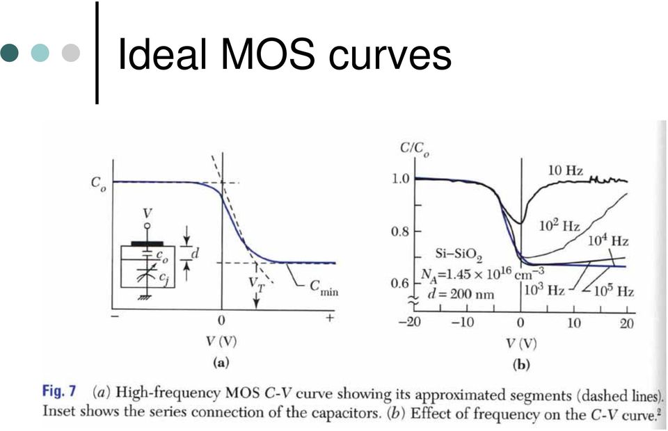
18 Ideal MOS curves 1.C=C o 2. 3.Threshold voltage

19 The SiO 2 -Si MOS diode In real case there are some difference between the ideal MOS a. the work function difference b. interface traps and oxide charges

20 The work function difference Flat-band voltage (V FB = ms )

21 Interface traps and oxide charges Interface-trapped charge Fixed-oxide charge Oxide-trapped charge Mobile ionic charge
22 Interface-trapped charge Q it It is due to the SiO 2 -Si interface properties and dependent on the chemical composition of this interface The interface trap density is orientation dependent for example in <100>orientation the interface trap density is about an order of magnitude smaller than that in <111>orientation 450 hydrogen annealing the value of Interface-trapped charges for <100>orientation silicon can be as low as cm -2
23 Fixed-oxide charge Q f the fixed-oxide charge is located within approximately 3 nm of the SiO 2 -Si interface.this charge is fixed and cannot be charged or discharged over a wide variation of surface potential. Generally, Q f is positive and depends on oxidation and annealing conditions and on silicon orientation It has been suggested that when the oxidation is stopped, some ionic silicon is left near the interface. It may result in the positive interface charge Q f Typical fixed-oxide charge densities for a carefully treated SiO 2 -Si interface system are about cm -2 for a <100>surface and about 5x cm -2 for a <111>surface
24 Oxide-trapped charge Q ot Oxide-trapped charge are associated with defect in the silicon dioxide. These charges can be created, for example, by X-ray radiation or high energy electron bombardment the trap are distributed inside the oxide layer. Most of process-related oxidetrapped charge can be removed by low-temperature annealing
25 Mobile ionic charge Q m The mobile ionic charges Q m, such as sodium or other alkali ion are mobile within the oxide under raisetemperature (e.g.>100) and highelectric field operation It may cause stability problem in device
26 Effect of a fixed oxide charge and interface traps on the C-V characteristics of an MOS diode
CHAPTER 10 Fundamentals of the Metal Oxide Semiconductor Field Effect Transistor
 CHAPTER 10 Fundamentals of the Metal Oxide Semiconductor Field Effect Transistor Study the characteristics of energy bands as a function of applied voltage in the metal oxide semiconductor structure known
Solid State Detectors = Semi-Conductor based Detectors
 Solid State Detectors = Semi-Conductor based Detectors Materials and their properties Energy bands and electronic structure Charge transport and conductivity Boundaries: the p-n junction Charge collection
Solar Photovoltaic (PV) Cells
 Cells") Solar Photovoltaic (PV) Cells A supplement topic to: Mi ti l S Micro-optical Sensors - A MEMS for electric power generation Science of Silicon PV Cells Scientific base for solar PV electric power generation
Solar Photovoltaic (PV) Cells A supplement topic to: Mi ti l S Micro-optical Sensors - A MEMS for electric power generation Science of Silicon PV Cells Scientific base for solar PV electric power generation
The MOSFET Transistor
 The MOSFET Transistor The basic active component on all silicon chips is the MOSFET Metal Oxide Semiconductor Field Effect Transistor Schematic symbol G Gate S Source D Drain The voltage on the gate controls
Fabrication and Characterization of N- and P-Type a-si:h Thin Film Transistors
 Fabrication and Characterization of N- and P-Type a-si:h Thin Film Transistors Engineering Practical Jeffrey Frederick Gold Fitzwilliam College University of Cambridge Lent 1997 FABRCATON AND CHARACTERZATON
Semiconductor doping. Si solar Cell
 Semiconductor doping Si solar Cell Two Levels of Masks - photoresist, alignment Etch and oxidation to isolate thermal oxide, deposited oxide, wet etching, dry etching, isolation schemes Doping - diffusion/ion
MOS Capacitor CHAPTER OBJECTIVES
 Hu_ch05v3.fm Page 157 Friday, February 13, 2009 2:38 PM 5 MOS Capacitor CHAPTER OBJECTIVES This chapter builds a deep understanding of the modern MOS (metal oxide semiconductor) structures. The key topics
CONTENTS. Preface. 1.1.2. Energy bands of a crystal (intuitive approach)
") CONTENTS Preface. Energy Band Theory.. Electron in a crystal... Two examples of electron behavior... Free electron...2. The particle-in-a-box approach..2. Energy bands of a crystal (intuitive approach)..3.
CONTENTS Preface. Energy Band Theory.. Electron in a crystal... Two examples of electron behavior... Free electron...2. The particle-in-a-box approach..2. Energy bands of a crystal (intuitive approach)..3.
Sheet Resistance = R (L/W) = R N ------------------ L
 = R N ------------------ L") Sheet Resistance Rewrite the resistance equation to separate (L / W), the length-to-width ratio... which is the number of squares N from R, the sheet resistance = (σ n t) - R L = -----------------------
Sheet Resistance Rewrite the resistance equation to separate (L / W), the length-to-width ratio... which is the number of squares N from R, the sheet resistance = (σ n t) - R L = -----------------------
Chapter 5. Second Edition ( 2001 McGraw-Hill) 5.6 Doped GaAs. Solution
 5.6 Doped GaAs. Solution") Chapter 5 5.6 Doped GaAs Consider the GaAs crystal at 300 K. a. Calculate the intrinsic conductivity and resistivity. Second Edition ( 2001 McGraw-Hill) b. In a sample containing only 10 15 cm -3 ionized
Chapter 5 5.6 Doped GaAs Consider the GaAs crystal at 300 K. a. Calculate the intrinsic conductivity and resistivity. Second Edition ( 2001 McGraw-Hill) b. In a sample containing only 10 15 cm -3 ionized
Crystalline solids. A solid crystal consists of different atoms arranged in a periodic structure.
 Crystalline solids A solid crystal consists of different atoms arranged in a periodic structure. Crystals can be formed via various bonding mechanisms: Ionic bonding Covalent bonding Metallic bonding Van
EDC Lesson 12: Transistor and FET Characteristics. 2008 EDCLesson12- ", Raj Kamal, 1
 EDC Lesson 12: Transistor and FET Characteristics Lesson-12: MOSFET (enhancement and depletion mode) Characteristics and Symbols 2008 EDCLesson12- ", Raj Kamal, 1 1. Metal Oxide Semiconductor Field Effect
An analytical gate tunneling current model for MOSFETs
 Физика и техника полупроводников, 2012, том 46, вып. 3 An analytical gate tunneling current model for MOSFETs Iman Abaspur Kazerouni, Seyed Ebrahim Hosseini Electrical and Computer Department, Sabzevar
SMA5111 - Compound Semiconductors Lecture 2 - Metal-Semiconductor Junctions - Outline Introduction
 SMA5111 - Compound Semiconductors Lecture 2 - Metal-Semiconductor Junctions - Outline Introduction Structure - What are we talking about? Behaviors: Ohmic, rectifying, neither Band picture in thermal equilibrium
The Physics of Energy sources Renewable sources of energy. Solar Energy
 The Physics of Energy sources Renewable sources of energy Solar Energy B. Maffei [email protected] Renewable sources 1 Solar power! There are basically two ways of using directly the radiative
Implementation Of High-k/Metal Gates In High-Volume Manufacturing
 White Paper Implementation Of High-k/Metal Gates In High-Volume Manufacturing INTRODUCTION There have been significant breakthroughs in IC technology in the past decade. The upper interconnect layers of
Bending, Forming and Flexing Printed Circuits
 Bending, Forming and Flexing Printed Circuits John Coonrod Rogers Corporation Introduction: In the printed circuit board industry there are generally two main types of circuit boards; there are rigid printed
ELEC 3908, Physical Electronics, Lecture 15. BJT Structure and Fabrication
 ELEC 3908, Physical Electronics, Lecture 15 Lecture Outline Now move on to bipolar junction transistor (BJT) Strategy for next few lectures similar to diode: structure and processing, basic operation,
LAB IV. SILICON DIODE CHARACTERISTICS
 LAB IV. SILICON DIODE CHARACTERISTICS 1. OBJECTIVE In this lab you are to measure I-V characteristics of rectifier and Zener diodes in both forward and reverse-bias mode, as well as learn to recognize
Semiconductors, diodes, transistors
 Semiconductors, diodes, transistors (Horst Wahl, QuarkNet presentation, June 2001) Electrical conductivity! Energy bands in solids! Band structure and conductivity Semiconductors! Intrinsic semiconductors!
Conductivity of silicon can be changed several orders of magnitude by introducing impurity atoms in silicon crystal lattice.
 CMOS Processing Technology Silicon: a semiconductor with resistance between that of conductor and an insulator. Conductivity of silicon can be changed several orders of magnitude by introducing impurity
Field Effect Transistors
 506 19 Principles of Electronics Field Effect Transistors 191 Types of Field Effect Transistors 193 Principle and Working of JFET 195 Importance of JFET 197 JFET as an Amplifier 199 Salient Features of
Fabrication and Characterization of Schottky Diode
 Fabrication and Characterization of Schottky Diode Arnab Dhabal Acknowledgements I would like to express my greatest gratitude to the people who have helped and supported me in this project. I wish to
Supercapacitors. Advantages Power density Recycle ability Environmentally friendly Safe Light weight
 Supercapacitors Supercapacitors also called ultracapacitors and electric double layer capacitors (EDLC) are capacitors with capacitance values greater than any other capacitor type available today. Capacitance
Photolithography. Class: Figure 12.1. Various ways in which dust particles can interfere with photomask patterns.
 Photolithography Figure 12.1. Various ways in which dust particles can interfere with photomask patterns. 19/11/2003 Ettore Vittone- Fisica dei Semiconduttori - Lectio XIII 16 Figure 12.2. Particle-size
Etching Etch Definitions Isotropic Etching: same in all direction Anisotropic Etching: direction sensitive Selectivity: etch rate difference between
 Etching Etch Definitions Isotropic Etching: same in all direction Anisotropic Etching: direction sensitive Selectivity: etch rate difference between 2 materials Other layers below one being etch Masking
FUNDAMENTAL PROPERTIES OF SOLAR CELLS
 FUNDAMENTAL PROPERTIES OF SOLAR CELLS January 31, 2012 The University of Toledo, Department of Physics and Astronomy SSARE, PVIC Principles and Varieties of Solar Energy (PHYS 4400) and Fundamentals of
Project 2B Building a Solar Cell (2): Solar Cell Performance
: Solar Cell Performance") April. 15, 2010 Due April. 29, 2010 Project 2B Building a Solar Cell (2): Solar Cell Performance Objective: In this project we are going to experimentally measure the I-V characteristics, energy conversion
April. 15, 2010 Due April. 29, 2010 Project 2B Building a Solar Cell (2): Solar Cell Performance Objective: In this project we are going to experimentally measure the I-V characteristics, energy conversion
High Open Circuit Voltage of MQW Amorphous Silicon Photovoltaic Structures
 High Open Circuit Voltage of MQW Amorphous Silicon Photovoltaic Structures ARGYRIOS C. VARONIDES Physics and EE Department University of Scranton 800 Linden Street, Scranton PA, 18510 United States Abstract:
Field-Effect (FET) transistors
 transistors") Field-Effect (FET) transistors References: Hayes & Horowitz (pp 142-162 and 244-266), Rizzoni (chapters 8 & 9) In a field-effect transistor (FET), the width of a conducting channel in a semiconductor and,
Field-Effect (FET) transistors References: Hayes & Horowitz (pp 142-162 and 244-266), Rizzoni (chapters 8 & 9) In a field-effect transistor (FET), the width of a conducting channel in a semiconductor and,
Solar Cell Parameters and Equivalent Circuit
 9 Solar Cell Parameters and Equivalent Circuit 9.1 External solar cell parameters The main parameters that are used to characterise the performance of solar cells are the peak power P max, the short-circuit
Matter, Materials, Crystal Structure and Bonding. Chris J. Pickard
 Matter, Materials, Crystal Structure and Bonding Chris J. Pickard Why should a theorist care? Where the atoms are determines what they do Where the atoms can be determines what we can do Overview of Structure
Junction FETs. FETs. Enhancement Not Possible. n p n p n p
 A11 An Introduction to FETs Introduction The basic principle of the field-effect transistor (FET) has been known since J. E. Lilienfeld s patent of 1925. The theoretical description of a FET made by hockley
UNIT I: INTRFERENCE & DIFFRACTION Div. B Div. D Div. F INTRFERENCE
 107002: EngineeringPhysics Teaching Scheme: Lectures: 4 Hrs/week Practicals-2 Hrs./week T.W.-25 marks Examination Scheme: Paper-50 marks (2 hrs) Online -50marks Prerequisite: Basics till 12 th Standard
High Rate Oxide Deposition onto Web by Reactive Sputtering from Rotatable Magnetrons
 High Rate Oxide Deposition onto Web by Reactive Sputtering from Rotatable Magnetrons D.Monaghan, V. Bellido-Gonzalez, M. Audronis. B. Daniel Gencoa, Physics Rd, Liverpool, L24 9HP, UK. www.gencoa.com,
Application Notes FREQUENCY LINEAR TUNING VARACTORS FREQUENCY LINEAR TUNING VARACTORS THE DEFINITION OF S (RELATIVE SENSITIVITY)
") FREQUENY LINEAR TUNING VARATORS FREQUENY LINEAR TUNING VARATORS For several decades variable capacitance diodes (varactors) have been used as tuning capacitors in high frequency circuits. Most of these
FREQUENY LINEAR TUNING VARATORS FREQUENY LINEAR TUNING VARATORS For several decades variable capacitance diodes (varactors) have been used as tuning capacitors in high frequency circuits. Most of these
Ultra-High Density Phase-Change Storage and Memory
 Ultra-High Density Phase-Change Storage and Memory by Egill Skúlason Heated AFM Probe used to Change the Phase Presentation for Oral Examination 30 th of May 2006 Modern Physics, DTU Phase-Change Material
Winbond W971GG6JB-25 1 Gbit DDR2 SDRAM 65 nm CMOS DRAM Process
 Winbond W971GG6JB-25 1 Gbit DDR2 SDRAM 65 nm CMOS DRAM Process Process Review For comments, questions, or more information about this report, or for any additional technical needs concerning semiconductor
Electric Field Mapping Lab 3. Precautions
 HB 09-25-07 Electric Field Mapping Lab 3 1 Electric Field Mapping Lab 3 Equipment mapping board, U-probe, resistive boards, templates, dc voltmeter (431B), 4 long leads, 16 V dc for wall strip Reading
Coating Technology: Evaporation Vs Sputtering
 Satisloh Italy S.r.l. Coating Technology: Evaporation Vs Sputtering Gianni Monaco, PhD R&D project manager, Satisloh Italy 04.04.2016 V1 The aim of this document is to provide basic technical information
Evaluation of the Surface State Using Charge Pumping Methods
 Evaluation of the Surface State Using Charge Pumping Methods Application Note 4156-9 Agilent 4155C/4156C Semiconductor Parameter Analyzer Introduction As device features get smaller, hot carrier induced
Understanding the p-n Junction by Dr. Alistair Sproul Senior Lecturer in Photovoltaics The Key Centre for Photovoltaic Engineering, UNSW
 Understanding the p-n Junction by Dr. Alistair Sproul Senior Lecturer in Photovoltaics The Key Centre for Photovoltaic Engineering, UNSW The p-n junction is the fundamental building block of the electronic
Nanotechnologies for the Integrated Circuits
 Nanotechnologies for the Integrated Circuits September 23, 2015 Dr. Bertrand Cambou Professor of Practice NAU, Cybersecurity School of Informatics, Computing, and Cyber-Systems Agenda The Market Silicon
Introduction to VLSI Fabrication Technologies. Emanuele Baravelli
 Introduction to VLSI Fabrication Technologies Emanuele Baravelli 27/09/2005 Organization Materials Used in VLSI Fabrication VLSI Fabrication Technologies Overview of Fabrication Methods Device simulation
Characteristics of blocking voltage for power 4H-SiC BJTs with mesa edge termination
 Vol. 31, No. 7 Journal of Semiconductors July 2010 Characteristics of blocking voltage for power 4H-SiC BJTs with mesa edge termination Zhang Qian( 张 倩 ), Zhang Yuming( 张 玉 明 ), and Zhang Yimen( 张 义 门
BJT Ebers-Moll Model and SPICE MOSFET model
 Department of Electrical and Electronic Engineering mperial College London EE 2.3: Semiconductor Modelling in SPCE Course homepage: http://www.imperial.ac.uk/people/paul.mitcheson/teaching BJT Ebers-Moll
Silicon Sensors for CMS Tracker at High-Luminosity Environment - Challenges in particle detection -
 [email protected] Finnish Society for Natural Philosophy, Helsinki, 17 February 2015 Silicon Sensors for CMS Tracker at High-Luminosity Environment - Challenges in particle detection - Timo Peltola
Lecture 030 DSM CMOS Technology (3/24/10) Page 030-1
 Page 030-1") Lecture 030 DSM CMOS Technology (3/24/10) Page 030-1 LECTURE 030 - DEEP SUBMICRON (DSM) CMOS TECHNOLOGY LECTURE ORGANIZATION Outline Characteristics of a deep submicron CMOS technology Typical deep submicron
Lecture 030 DSM CMOS Technology (3/24/10) Page 030-1 LECTURE 030 - DEEP SUBMICRON (DSM) CMOS TECHNOLOGY LECTURE ORGANIZATION Outline Characteristics of a deep submicron CMOS technology Typical deep submicron
Tobias Märkl. November 16, 2009
 ,, Tobias Märkl to 1/f November 16, 2009 1 / 33 Content 1 duction to of Statistical Comparison to Other Types of Noise of of 2 Random duction to Random General of, to 1/f 3 4 2 / 33 , to 1/f 3 / 33 What
Exam 2 Practice Problems Part 1 Solutions
 MASSACHUSETTS INSTITUTE OF TECHNOLOGY Department of Physics Exam Practice Problems Part 1 Solutions Problem 1 Electric Field and Charge Distributions from Electric Potential An electric potential V ( z
Chapter 2 The Study on Polycrystalline Pentacene Thin Film Transistors
 Chapter 2 The Study on Polycrystalline Pentacene Thin Film Transistors 2.1 Introduction Recent focus and attention on organic thin film transistors (TFTs) resulted in dramatic performance improvements
SFxxx-S PID Test Report (Potential Induced Degradation) TUV Rheinland Japan. ARC Product Management 2015.07 Ver. 1
 TUV Rheinland Japan. ARC Product Management 2015.07 Ver. 1") SFxxx-S PID Test Report (Potential Induced Degradation) TUV Rheinland Japan ARC Product Management 2015.07 Ver. 1 Outline SLIDE 1 2 Outline What is PID? TOPICS 3 4 5 6 7 8 Principle of PID & resistance
SFxxx-S PID Test Report (Potential Induced Degradation) TUV Rheinland Japan ARC Product Management 2015.07 Ver. 1 Outline SLIDE 1 2 Outline What is PID? TOPICS 3 4 5 6 7 8 Principle of PID & resistance
Characteristic curves of a solar cell
 Related Topics Semi-conductor, p-n junction, energy-band diagram, Fermi characteristic energy level, diffusion potential, internal resistance, efficiency, photo-conductive effect, acceptors, donors, valence
OLED display. Ying Cao
 OLED display Ying Cao Outline OLED basics OLED display A novel method of fabrication of flexible OLED display Potentials of OLED Suitable for thin, lightweight, printable displays Broad color range Good
3. Diodes and Diode Circuits. 3. Diodes and Diode Circuits TLT-8016 Basic Analog Circuits 2005/2006 1
 3. Diodes and Diode Circuits 3. Diodes and Diode Circuits TLT-8016 Basic Analog Circuits 2005/2006 1 3.1 Diode Characteristics Small-Signal Diodes Diode: a semiconductor device, which conduct the current
AN3022. Establishing the Minimum Reverse Bias for a PIN Diode in a High-Power Switch. 1. Introduction. Rev. V2
 Abstract - An important circuit design parameter in a high-power p-i-n diode application is the selection of an appropriate applied dc reverse bias voltage. Until now, this important circuit parameter
Chapter 7: Polarization
 Chapter 7: Polarization Joaquín Bernal Méndez Group 4 1 Index Introduction Polarization Vector The Electric Displacement Vector Constitutive Laws: Linear Dielectrics Energy in Dielectric Systems Forces
Theory of Transistors and Other Semiconductor Devices
 Theory of Transistors and Other Semiconductor Devices 1. SEMICONDUCTORS 1.1. Metals and insulators 1.1.1. Conduction in metals Metals are filled with electrons. Many of these, typically one or two per
Lecture 12. Physical Vapor Deposition: Evaporation and Sputtering Reading: Chapter 12. ECE 6450 - Dr. Alan Doolittle
 Lecture 12 Physical Vapor Deposition: Evaporation and Sputtering Reading: Chapter 12 Evaporation and Sputtering (Metalization) Evaporation For all devices, there is a need to go from semiconductor to metal.
Fig6-22 CB configuration. Z i [6-54] Z o [6-55] A v [6-56] Assuming R E >> r e. A i [6-57]
![Fig6-22 CB configuration. Z i [6-54] Z o [6-55] A v [6-56] Assuming R E >> r e. A i [6-57]](/thumbs/40/21338705.jpg "Fig6-22 CB configuration. Z i [6-54] Z o [6-55] A v [6-56] Assuming R E >> r e. A i [6-57]") Common-Base Configuration (CB) The CB configuration having a low input and high output impedance and a current gain less than 1, the voltage gain can be quite large, r o in MΩ so that ignored in parallel
Common-Base Configuration (CB) The CB configuration having a low input and high output impedance and a current gain less than 1, the voltage gain can be quite large, r o in MΩ so that ignored in parallel
PARTICLE SIMULATION ON MULTIPLE DUST LAYERS OF COULOMB CLOUD IN CATHODE SHEATH EDGE
 PARTICLE SIMULATION ON MULTIPLE DUST LAYERS OF COULOMB CLOUD IN CATHODE SHEATH EDGE K. ASANO, S. NUNOMURA, T. MISAWA, N. OHNO and S. TAKAMURA Department of Energy Engineering and Science, Graduate School
A Remote Plasma Sputter Process for High Rate Web Coating of Low Temperature Plastic Film with High Quality Thin Film Metals and Insulators
 A Remote Plasma Sputter Process for High Rate Web Coating of Low Temperature Plastic Film with High Quality Thin Film Metals and Insulators Dr Peter Hockley and Professor Mike Thwaites, Plasma Quest Limited
Computer Simulations of Edge Effects in a Small-Area Mesa N-P Junction Diode
 Computer Simulations of Edge Effects in a Small-Area Mesa N-P Junction Diode Preprint Conference Paper NREL/CP-520-45002 February 2009 J. Appel and B. Sopori National Renewable Energy Laboratory N.M. Ravindra
Gamma and X-Ray Detection
 Gamma and X-Ray Detection DETECTOR OVERVIEW The kinds of detectors commonly used can be categorized as: a. Gas-filled Detectors b. Scintillation Detectors c. Semiconductor Detectors The choice of a particular
Measurement of Capacitance
 Measurement of Capacitance Pre-Lab Questions Page Name: Class: Roster Number: Instructor:. A capacitor is used to store. 2. What is the SI unit for capacitance? 3. A capacitor basically consists of two
FEATURE ARTICLE. Figure 1: Current vs. Forward Voltage Curves for Silicon Schottky Diodes with High, Medium, Low and ZBD Barrier Heights
 PAGE 1 FEBRUARY 2009 Schottky Diodes by Rick Cory, Skyworks Solutions, Inc. Introduction Schottky diodes have been used for several decades as the key elements in frequency mixer and RF power detector
Silicon-On-Glass MEMS. Design. Handbook
 Silicon-On-Glass MEMS Design Handbook A Process Module for a Multi-User Service Program A Michigan Nanofabrication Facility process at the University of Michigan March 2007 TABLE OF CONTENTS Chapter 1...
XI / PHYSICS FLUIDS IN MOTION 11/PA
 Viscosity It is the property of a liquid due to which it flows in the form of layers and each layer opposes the motion of its adjacent layer. Cause of viscosity Consider two neighboring liquid layers A
Transistor Characteristics and Single Transistor Amplifier Sept. 8, 1997
 Physics 623 Transistor Characteristics and Single Transistor Amplifier Sept. 8, 1997 1 Purpose To measure and understand the common emitter transistor characteristic curves. To use the base current gain
Observation of Long Transients in the Electrical Characterization of Thin Film BST Capacitors
 Integrated Ferroelectrics, 53: 503 511, 2003 Copyright C Taylor & Francis Inc. ISSN: 1058-4587 print/ 1607-8489 online DOI: 10.1080/10584580390258651 Observation of Long Transients in the Electrical Characterization
Looking at Capacitors
 Module 2 AC Theory Looking at What you'll learn in Module 2: In section 2.1 Common capacitor types and their uses. Basic Circuit Symbols for. In section 2.2 Charge & Discharge How capacitors work. What
Use of Carbon Nanoparticles for the Flexible Circuits Industry
 Use of Carbon Nanoparticles for the Flexible Circuits Industry Ying (Judy) Ding, Rich Retallick MacDermid, Inc. Waterbury, Connecticut Abstract FPC (Flexible Printed Circuit) has been growing tremendously
Wafer Manufacturing. Reading Assignments: Plummer, Chap 3.1~3.4
 Wafer Manufacturing Reading Assignments: Plummer, Chap 3.1~3.4 1 Periodic Table Roman letters give valence of the Elements 2 Why Silicon? First transistor, Shockley, Bardeen, Brattain1947 Made by Germanium
Peltier Application Note
 Peltier Application Note Early 19th century scientists, Thomas Seebeck and Jean Peltier, first discovered the phenomena that are the basis for today s thermoelectric industry. Seebeck found that if you
An organic semiconductor is an organic compound that possesses similar
 MSE 542 Final Term Paper Title: Organic Semiconductor for Flexible Electronics Name: Chunhung Huang Introduction: An organic semiconductor is an organic compound that possesses similar properties to inorganic
CO2005: Electronics I (FET) Electronics I, Neamen 3th Ed. 1
 Electronics I, Neamen 3th Ed. 1") CO2005: Electronics I The Field-Effect Transistor (FET) Electronics I, Neamen 3th Ed. 1 MOSFET The metal-oxide-semiconductor field-effect transistor (MOSFET) becomes a practical reality in the 1970s. The
CO2005: Electronics I The Field-Effect Transistor (FET) Electronics I, Neamen 3th Ed. 1 MOSFET The metal-oxide-semiconductor field-effect transistor (MOSFET) becomes a practical reality in the 1970s. The
Chapter 6. Current and Resistance
 6 6 6-0 Chapter 6 Current and Resistance 6.1 Electric Current... 6-2 6.1.1 Current Density... 6-2 6.2 Ohm s Law... 6-5 6.3 Summary... 6-8 6.4 Solved Problems... 6-9 6.4.1 Resistivity of a Cable... 6-9
Development of New Inkjet Head Applying MEMS Technology and Thin Film Actuator
 Development of New Inkjet Head Applying MEMS Technology and Thin Film Actuator Kenji MAWATARI, Koich SAMESHIMA, Mitsuyoshi MIYAI, Shinya MATSUDA Abstract We developed a new inkjet head by applying MEMS
Power Resistor for Mounting onto a Heatsink Thick Film Technology
 DIMENSIONS in millimeters Power Resistor for Mounting onto a Heatsink Thick Film Technology FEATURES 800 W at 85 C bottom case temperature Wide resistance range: 0.3 to 900 k E24 series Non inductive Easy
Physics 623 Transistor Characteristics and Single Transistor Amplifier Sept. 13, 2006
 Physics 623 Transistor Characteristics and Single Transistor Amplifier Sept. 13, 2006 1 Purpose To measure and understand the common emitter transistor characteristic curves. To use the base current gain
Bipolar Junction Transistor Basics
 by Kenneth A. Kuhn Sept. 29, 2001, rev 1 Introduction A bipolar junction transistor (BJT) is a three layer semiconductor device with either NPN or PNP construction. Both constructions have the identical
Solid-State Physics: The Theory of Semiconductors (Ch. 10.6-10.8) SteveSekula, 30 March 2010 (created 29 March 2010)
 SteveSekula, 30 March 2010 (created 29 March 2010)") Modern Physics (PHY 3305) Lecture Notes Modern Physics (PHY 3305) Lecture Notes Solid-State Physics: The Theory of Semiconductors (Ch. 10.6-10.8) SteveSekula, 30 March 2010 (created 29 March 2010) Review
Modern Physics (PHY 3305) Lecture Notes Modern Physics (PHY 3305) Lecture Notes Solid-State Physics: The Theory of Semiconductors (Ch. 10.6-10.8) SteveSekula, 30 March 2010 (created 29 March 2010) Review
Electromagnetism Laws and Equations
 Electromagnetism Laws and Equations Andrew McHutchon Michaelmas 203 Contents Electrostatics. Electric E- and D-fields............................................. Electrostatic Force............................................2
HW6 Solutions Notice numbers may change randomly in your assignments and you may have to recalculate solutions for your specific case.
 HW6 Solutions Notice numbers may change randomly in your assignments and you may have to recalculate solutions for your specific case. Tipler 22.P.053 The figure below shows a portion of an infinitely
Modeling the Characteristics of a High-k HfO 2 -Ta 2 O 5 Capacitor in Verilog-A
 Modeling the Characteristics of a High-k HfO 2 -Ta 2 O 5 Capacitor in Verilog-A George V. Angelov, Member, IEEE Abstract A circuit simulation model of a MOS capacitor with high-k HfO 2 Ta 2 O 5 mixed layer
Diode Circuits. Operating in the Reverse Breakdown region. (Zener Diode)
") Diode Circuits Operating in the Reverse Breakdown region. (Zener Diode) In may applications, operation in the reverse breakdown region is highly desirable. The reverse breakdown voltage is relatively insensitive
Diode Circuits Operating in the Reverse Breakdown region. (Zener Diode) In may applications, operation in the reverse breakdown region is highly desirable. The reverse breakdown voltage is relatively insensitive
Special-Purpose Diodes
 7 Special-Purpose Diodes 7.1 Zener Diode 7.2 Light-Emitting Diode (LED) 7.3 LED Voltage and Current 7.4 Advantages of LED 7.5 Multicolour LEDs 7.6 Applications of LEDs 7.7 Photo-diode 7.8 Photo-diode operation
Data Sheet. Nationstar LED
 Data Sheet Nationstar LED 1 Table of Contents General Informations:... 3 Electrical and Flux Characteristics... 3 Color Wavelength Diagram:... 6 Mechanical Dimensions:... 7 Electrical Connection:... 7
Measuring Silicon and Germanium Band Gaps using Diode Thermometers
 Measuring Silicon and Germanium Band Gaps using Diode Thermometers Haris Amin Department of Physics, Wabash College, Crawfordsville, IN 47933 (Dated: April 11, 2007) This paper reports the band gaps of
A Potentiometric Analysis of Fluoride Ion in Toothpaste
 CHEM 311L Quantitative Analysis Laboratory Revision 2.0 A Potentiometric Analysis of Fluoride Ion in Toothpaste In this laboratory exercise, we will analyze a toothpaste sample for its Fluoride Ion (F
Formation of solids from solutions and melts
 Formation of solids from solutions and melts Solids from a liquid phase. 1. The liquid has the same composition as the solid. Formed from the melt without any chemical transformation. Crystallization and
ENEE 313, Spr 09 Midterm II Solution
 ENEE 313, Spr 09 Midterm II Solution PART I DRIFT AND DIFFUSION, 30 pts 1. We have a silicon sample with non-uniform doping. The sample is 200 µm long: In the figure, L = 200 µm= 0.02 cm. At the x = 0
Here we introduced (1) basic circuit for logic and (2)recent nano-devices, and presented (3) some practical issues on nano-devices.
 basic circuit for logic and (2)recent nano-devices, and presented (3) some practical issues on nano-devices.") Outline Here we introduced () basic circuit for logic and (2)recent nano-devices, and presented (3) some practical issues on nano-devices. Circuit Logic Gate A logic gate is an elemantary building block
Outline Here we introduced () basic circuit for logic and (2)recent nano-devices, and presented (3) some practical issues on nano-devices. Circuit Logic Gate A logic gate is an elemantary building block
Optical Hyperdoping: Transforming Semiconductor Band Structure for Solar Energy Harvesting
 Optical Hyperdoping: Transforming Semiconductor Band Structure for Solar Energy Harvesting 3G Solar Technologies Multidisciplinary Workshop MRS Spring Meeting San Francisco, CA, 5 April 2010 Michael P.
Quartz Glass. Tubes and Rods
 Quartz Glass Tubes and Rods PH 300, GE 214, QI PN GVB Solutions in Glass Schlackstrasse 3 52080 Aachen Germany +49-241/9108588 +49-241/9108589 E- [email protected] www.g-v-b.de Table of contents General Information
APPLICATION NOTES: Dimming InGaN LED
 APPLICATION NOTES: Dimming InGaN LED Introduction: Indium gallium nitride (InGaN, In x Ga 1-x N) is a semiconductor material made of a mixture of gallium nitride (GaN) and indium nitride (InN). Indium