Ultra-High Density Phase-Change Storage and Memory
|
|
|
- Randell Rich
- 10 years ago
- Views:
Transcription
1 Ultra-High Density Phase-Change Storage and Memory by Egill Skúlason Heated AFM Probe used to Change the Phase Presentation for Oral Examination 30 th of May 2006 Modern Physics, DTU Phase-Change Material

2 Outline Introduction Memory vs Storage Changes in Data Storage Phase-Change Memory and Storage Resent Developments in the PC Concepts Ultra-High-Density PC Memory (IBM, Nat. Mat. 2006) Phase-Change Line-Cell Memory (Philips, Nat. Mat. 2005) Summary 2
 Phase-Change Line-Cell Memory (Philips, Nat. Mat.")
3 Memory vs Storage Computer memory and storage Components, devices and recording media that retain data for some interval of time (e.g. operation, text, picture or audio) Represents the information in the form of binary digits 1s and 0s Memory Usually solid state storage known as RAM Or other forms of fast but temporary storage (primary storage) Storage Slower than primary storage but of more permanent nature Optical disks or magnetic storage (hard disks) So far, no practical universal storage medium exists All forms of storage have some drawbacks Computer systems usually contain several kinds of storage, each with an individual purpose 3

4 Changes in Data Storage (1) Paper tape and punch cards (1890s) Recorded by punching holes into paper or cardboard medium Read electrically or optically (solid or hole?) Magnetic storage (1950s) Different patterns of magnetization (non-volatile) Accessed using one or more read/write heads (sequential access) e.g. floppy disk, hard disk and magnetic tape 4
 e.g. floppy disk, hard disk and magnetic tape 4")
5 Changes in Data Storage (2) Semiconductor (SC) storage (~1960) Integrated circuits used to store information A chip with millions of tiny transistors Modern computers: primary storage consists of dynamic volatile SC memory or dynamic RAM Recently, non-volatile SC memory (flash) for offline storage in home computers Optical disk storage (patent1960s, later commercial) Tiny pits etched on the surface of a circular disk Read by illuminating the surface with a laser diode and observing the reflection Non-volatile and sequential accessed e.g. CD s and DVD s 5

6 Changes in Data Storage (3) Magneto-optical disk storage (late 1980s) The magnetic state on a ferromagnetic surface stores information Read optically and written by combining magnetic and optical methods Non-volatile, sequential access, slow write and fast read Recently proposed methods Molecular memory: stores information in organic molecules that can store electric charge (primary storage) Phase-change memory: different mechanical phases of materials used to store information Read information by observing varying electric resistance Non-volatile, random access, read/write storage Might be used as primary, secondary and off-line storage 6

7 Phase-Change Memory and Storage Phase-change memory from atomic order (crystalline) to disorder (amorphous) was found by S.R. Ovshinsky in the 1960s, called Ovonic memory The material is a chalcogenide alloy of Ge, Sb and Te (GST), already widely used in optical disks and SC memories Million overwrite PC technology enabled rewritable DVD When the structure changes from amorphous to crystalline, the optical absorption edge of the material shifts to a longer wavelength The two phases also have dramatically different electrical resistivity and these properties form the basis by which data is stored The amorphous, high resistance state is used to represent a binary 1, and the crystalline, low resistance state represents a binary 0 7

8 Amorphizing and Crystallizing the GST Phase-change materials (GST), are technologically very important for read-write optical and electrical storage, because they can be switched rapidly back and forth between amorphous and crystalline phases by applying appropriate heat pulses (optical or electrical) GST can be amorphized by a short pulsed heating (~10 ns) above the melting temperature (~600 C) with subsequent rapid cooling (~10 9 K/s) Recrystallization is achieved by a slightly longer heat pulse (~100 ns) below the melting temperature but above the glass-transition temperature (~200 C) 8
 Recrystallization is achieved by a slightly longer heat pulse (~100 ns) below the melting temperature but above the glass-transition")
9 Outline Introduction Memory vs Storage Changes in Data Storage Phase-Change Memory and Storage Resent Developments in the PC Concepts Ultra-High-Density PC Memory (IBM, Nat. Mat. 2006) Phase-Change Line-Cell Memory (Philips, Nat. Mat. 2005) Summary 9
 Phase-Change Line-Cell Memory (Philips, Nat. Mat.")
10 Writing Nanoscale Bits Scanned probe and other methods have showed that it is technically difficult to provide and control the required heating (~50 MW m -2 K -1 ) at densities above ~1 Tb/inch 2 In many cases, adjacent bit erasure, limits the achievable storage densities, whereas other methods, such as near-field optical techniques, suffer from low throughput and insufficient heating at small bit sizes The research team from IBM have managed to write ultrahigh-density bit pattern by locally heating the GST material with a tip of an AFM They have also designed a nanoheater as an alternative to the heated AFM tip 10

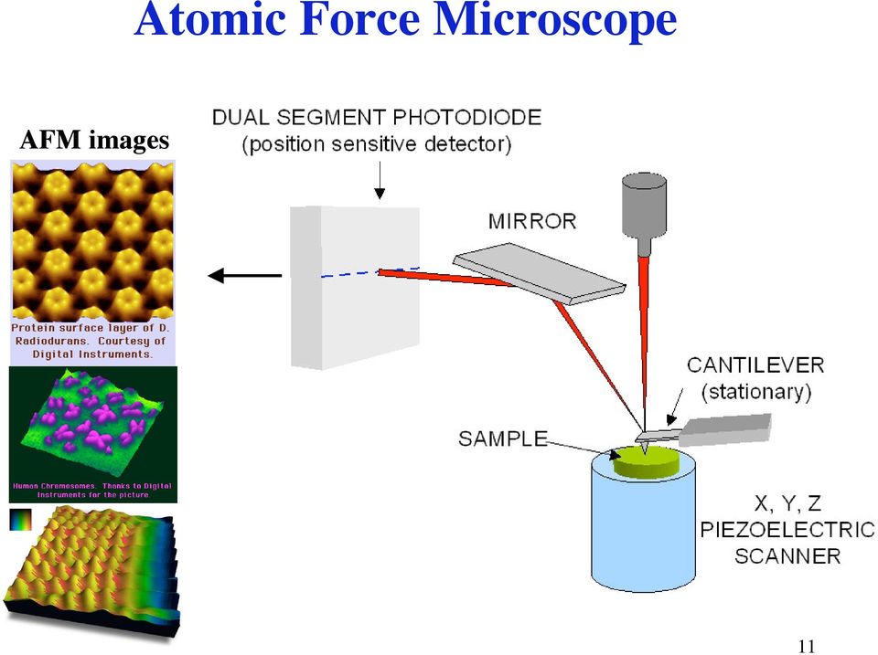
11 Atomic Force Microscope AFM images 11
12 Thermal Recording of Ultra-High-Density Phase-Change Bit Patterns Experimental setup: Laser pulsed heated AFM tip -> ultra small (d: < 5 nm) heat source Crystalline bits visible as little valleys because their density is higher than that of the amorphous phase 0.4 Tb/inch 2 40 nm pitch between bits Line profile of the PC bits: 7 A height difference Hamann et al, Nature Materials, 5 (2006) 12

13 Ultra-High-Density PC Bit Patterns 0.4 Tb/inch2 1.6 Tb/inch2 Part of a 1.6 Tb/inch2 bit pattern erased crystalline Previously erased bit pattern rewritten at 3.3 Tb/inch2 3 orders of magnitude denser than with commercial optical storage technology amorphous Hamann et al, Nature Materials, 5 (2006) 13

14 The Nanoheater This thin-film resistive nanoheater can reliably generate hot-spots with dimensions of less than 50 nm -> might be technically viable alternative to the heated AFM tip AFM image of the nanoheater Design: Advanced electron-beam lithography used to fabricate thinfilm (~25 nm thick) Pt substrates The total heater size is 1 x 3 µm 2 Hamann et al, Nature Materials, 5 (2006) 14
 Pt substrates The total heater size is 1 x 3 µm 2 Hamann et al, Nature Materials,")
15 Nanoheater Thermal Properties Temperature image Characterizing the temperature distribution of the nanoheater: They raster-scanned a cold AFM tip (in a tapping mode) over the powered-up heater, while monitoring its temperature-dependent resistance Finite-Element Calculations Evidently the resistance-change drops laterally away from the heater quite sharply (hot-spot < 50 nm) -> Consistent with standard FE calculations Hamann et al, Nature Materials, 5 (2006) 15
 -> Consistent with standard FE calculations Hamann et al, Nature")
16 Nanoheater Thermal Properties Heat transfer to the nanoheater: By applying more power to the nanoheater, its temperature increases -> determine a thermal resistance of ~ 1.1 K/µW for a typical nanoheater -> In excellent agreement with finite element (FE) calculations Hamann et al, Nature Materials, 5 (2006) 16

17 An All-Thermal Memory/Storage Concept The heater is directly patterned on a PC film Recording by applying appropriate current pulses Amorphizing: 10 ns 1.5 V Crystallizing: 100 ns 0.7 V 2 ohms Reading by measuring the phase-dependent thermal resistance of the heater with low bias-current (5.1 ma) Hamann et al, Nature Materials, 5 (2006) 10 4 cycles doable but the baseline drifts ca. 30% -> better heater design and drive electronics 17
 Hamann et al, Nature Materials, 5 (2006) 10 4 cycles doable but the baseline drifts ca.")
18 Outline Introduction Memory vs Storage Changes in Data Storage Phase-Change Memory and Storage Resent Developments in the PC Concepts Ultra-High-Density PC Memory (IBM, Nat. Mat. 2006) Phase-Change Line-Cell Memory (Philips, Nat. Mat. 2005) Summary 18
 Phase-Change Line-Cell Memory (Philips, Nat. Mat.")
19 Design of PC-RAM Cell An individual PC-RAM memory cell cannot be based on PC volume alone Current designs have transistors and a resistor associated with each cell The PC volume is normally contacted top and bottom, but the relatively large cross-section of such cells leads to high power consumption It is therefore of interest to try geometries in which the current is lateral rather than vertical The research team from Philips have designed a new type of cell to write the PC bit pattern, which they call the phase-change line cell memory 19

20 Concepts for PC Non-Volatile Memories The part of the PC layer undergoing the reversible PC transition is shown in red The dielectric surrounding are denoted in blue Expected that PC in the LC will appear within the line -> there the current density and temperature rise will by largest Advances of line cells over OUM: - No special electrodes are needed. - Only dielectric material (SiO 2 ) surrounds the portion of the film undergoing PC -> lower programming power and current Lankhorst et al, Nature Materials, 4 (2005) 20
 surrounds the portion of the film undergoing PC -> lower programming power and current")
21 PC Memory Cells used to test Feasibility of Line Concept Cross-section of a line-concept memory cell with TiN contacts and Al bondpads processed on a silicon wafer Scanning electron micrograph of such a cell (length 500 nm, width 50 nm) made after structuring of the PC layer, which is done by electron-beam lithography Inset, detail of similar cell with dimensions ca. 100 nm by 50 nm Lankhorst et al, Nature Materials, 4 (2005) 21
22 Phase-Change Materials used in Optical and Electrical Memories In this PC line memory study, they use a Sb-Te composition, doped with Ge, In, Ag and/or Ga Usually, OUM device studies use the Ge 2 Sb 2 Te 5 composition Lankhorst et al, Nature Materials, 4 (2005) 22
23 Temperature Dependent Resistivity of Phase- Change Films with the Line Cell Concept Electrical and structural properties of Ge 2 Sb 2 Te 5 and doped SbTe materials Both materials show large difference in resistivity between the amorphous and the crystalline states Amorphous Ge 2 Sb 2 Te 5 film crystallizes first into a cubic state and above 300 C into more stable hexagonal state Doped SbTe film crystallizes directly into hexagonal state -> better suited in the line cell concept Lankhorst et al, Nature Materials, 4 (2005) 23
24 Typical Line-Cell Electrical Characteristics d.c. Cell Resistance with 50 ns Pulses Crystalline state: Large increase in resistance observed when applying voltage pulses above the RESET threshold voltage -> becomes amorphous Amorphous state: At voltage pulses in the SET window the phase is crystallized and after the SET window it is amorphized again The difference between the incompletely recrystallized state and the amorphous state is large enough for reading the cell Lankhorst et al, Nature Materials, 4 (2005) 24
25 Feasibility of Fast and Reversible Programming of PC-LC with Low Power Real time oscilloscope traces between low ohmic crystalline and high ohmic amorphous state Similar experiments on cells with various line length have shown that the required SET pulse time for complete recrystallization of the amorphous state decreases with decreasing line length -> The speed of the memory thus increases by decreasing the cell PC-LC: 200 nm, cross section ~20 2 nm 2 Read pulse: 0.3 V and 30 ns Black: voltage applied over the cell Red: resulting current Programming time (crystallizaiton) : Real LCM doped-sbte: ns Real OUM GST: ns 25 Lankhorst et al, Nature Materials, 4 (2005)
26 Cycle Endurance of the LC PC-LC: 100 nm, cross section ~25 2 nm 2 Lankhorst et al, Nature Materials, 4 (2005) d.c. cell- resistance are measured after applying a single RESET and a single SET pulse Typically 10 6 cycles are achieved At 10 7 cycles or more, the RESET pulse no longer leads to amorphization and in addition d.c. cell resistance has decreased At cycles the LC is dead The desired value is but 10 6 cycles are similar to flash memory For OUM, typically cycles are reported Might be possible to improve the LC by optimizing materials and cell design 26
27 Scaling of Line-Cell Length Measured RESET voltages (circles) & maximum threshold voltage (triangles) as a function length of lines The RESET voltage decreases with decreasing line length The shortest lines begin to show a reversal of this trend, caused by a relatively large heat loss at the pads at the end of the line Maximum threshold voltages are determined for cells that have been programmed into the maximal possible RESET resistance -> V T increases with increased line length Low enough for cells shorter than 200 nm Lankhorst et al, Nature Materials, 4 (2005) 27
28 Scaling of Cross-Section & Line-Cell Length RESET current can be reduced by scaling-down the cross-section of the line The measured currents agree with the trend obtained from numerical calculations (except the 80 and 100 nm lines) Dashed lines: 2D numerical calculations on cylindrical lines (home made program to solve differential equations) Lankhorst et al, Nature Materials, 4 (2005) Further reduction of programming current is possible by using better thermal insulation material 28
29 Summary Similar idea to store information for more then 100 years, from the paper tape to the phase-change materials Using AFM, it is possible to write 3.3 Tb/inch2 pattern which is 3 orders of magnitude denser than commercially available today and 3 times denser than previously published for PC memory Designing a nanoheater as an alternative to the AFM tip, it is possible to read, write and erase GST film many times 29
30 Designing the PC cell where the current is laterally instead of vertically and doping the SbTe material gives promising results Summary The PC material can easily been distinguished between amorphous and crystalline phases and this LC can run for million cycles Conclusion PC materials have the potential to become universal memory devices in near future technology 30
Storage Class Memory and the data center of the future
 IBM Almaden Research Center Storage Class Memory and the data center of the future Rich Freitas HPC System performance trends System performance requirement has historically double every 18 mo and this
Overview of Optical Recording Technology- Current Status and Near Term Projections
 Overview of Optical Recording Technology- Current Status and Near Term Projections Koichi Sadashige Sadashige Associates 15 Amherst Rd, Voorhees NJ 08043-4901 Phone: +1-856-767-2644, FAX: +1-856-767-1462
Writing Assignment #2 due Today (5:00pm) - Post on your CSC101 webpage - Ask if you have questions! Lab #2 Today. Quiz #1 Tomorrow (Lectures 1-7)
 - Post on your CSC101 webpage - Ask if you have questions! Lab #2 Today. Quiz #1 Tomorrow (Lectures 1-7)") Overview of Computer Science CSC 101 Summer 2011 Main Memory vs. Auxiliary Storage Lecture 7 July 14, 2011 Announcements Writing Assignment #2 due Today (5:00pm) - Post on your CSC101 webpage - Ask if
Overview of Computer Science CSC 101 Summer 2011 Main Memory vs. Auxiliary Storage Lecture 7 July 14, 2011 Announcements Writing Assignment #2 due Today (5:00pm) - Post on your CSC101 webpage - Ask if
Nanotechnologies for the Integrated Circuits
 Nanotechnologies for the Integrated Circuits September 23, 2015 Dr. Bertrand Cambou Professor of Practice NAU, Cybersecurity School of Informatics, Computing, and Cyber-Systems Agenda The Market Silicon
Chapter 8 Memory Units
 Chapter 8 Memory Units Contents: I. Introduction Basic units of Measurement II. RAM,ROM,PROM,EPROM Storage versus Memory III. Auxiliary Storage Devices-Magnetic Tape, Hard Disk, Floppy Disk IV.Optical
Main Memory & Backing Store. Main memory backing storage devices
 Main Memory & Backing Store Main memory backing storage devices 1 Introduction computers store programs & data in two different ways: nmain memory ntemporarily stores programs & data that are being processed
Implementation Of High-k/Metal Gates In High-Volume Manufacturing
 White Paper Implementation Of High-k/Metal Gates In High-Volume Manufacturing INTRODUCTION There have been significant breakthroughs in IC technology in the past decade. The upper interconnect layers of
Local Heating Attacks on Flash Memory Devices. Dr Sergei Skorobogatov
 Local Heating Attacks on Flash Memory Devices Dr Sergei Skorobogatov http://www.cl.cam.ac.uk/~sps32 email: [email protected] Introduction Semi-invasive attacks were introduced in 2002 ( Optical fault induction
CSCA0102 IT & Business Applications. Foundation in Business Information Technology School of Engineering & Computing Sciences FTMS College Global
 CSCA0102 IT & Business Applications Foundation in Business Information Technology School of Engineering & Computing Sciences FTMS College Global Chapter 2 Data Storage Concepts System Unit The system unit
Flash Memories. João Pela (52270), João Santos (55295) December 22, 2008 IST
, João Santos (55295) December 22, 2008 IST") Flash Memories João Pela (52270), João Santos (55295) IST December 22, 2008 João Pela (52270), João Santos (55295) (IST) Flash Memories December 22, 2008 1 / 41 Layout 1 Introduction 2 How they work 3
Flash Memories João Pela (52270), João Santos (55295) IST December 22, 2008 João Pela (52270), João Santos (55295) (IST) Flash Memories December 22, 2008 1 / 41 Layout 1 Introduction 2 How they work 3
CSCA0201 FUNDAMENTALS OF COMPUTING. Chapter 5 Storage Devices
 CSCA0201 FUNDAMENTALS OF COMPUTING Chapter 5 Storage Devices 1 1. Computer Data Storage 2. Types of Storage 3. Storage Device Features 4. Other Examples of Storage Device 2 Storage Devices A storage device
MOS (metal-oxidesemiconductor) 李 2003/12/19
 李 2003/12/19") MOS (metal-oxidesemiconductor) 李 2003/12/19 Outline Structure Ideal MOS The surface depletion region Ideal MOS curves The SiO 2 -Si MOS diode (real case) Structure A basic MOS consisting of three layers.
MOS (metal-oxidesemiconductor) 李 2003/12/19 Outline Structure Ideal MOS The surface depletion region Ideal MOS curves The SiO 2 -Si MOS diode (real case) Structure A basic MOS consisting of three layers.
A+ Guide to Managing and Maintaining Your PC, 7e. Chapter 1 Introducing Hardware
 A+ Guide to Managing and Maintaining Your PC, 7e Chapter 1 Introducing Hardware Objectives Learn that a computer requires both hardware and software to work Learn about the many different hardware components
Computer Systems Structure Main Memory Organization
 Computer Systems Structure Main Memory Organization Peripherals Computer Central Processing Unit Main Memory Computer Systems Interconnection Communication lines Input Output Ward 1 Ward 2 Storage/Memory
Optical Storage Technology. Optical Disc Storage
 Optical Storage Technology Optical Disc Storage Introduction Since the early 1940s, magnetic recording has been the mainstay of electronic information storage worldwide. Magnetic tape has been used extensively
Digital Image Formation. Storage Technology
 Digital Image Formation Storage Technology Storage Technology Quiz Name one type of data storage?! Storage Technology Data Storage Device is a device for recording (storing) information (data).!! Recording
Handout 17. by Dr Sheikh Sharif Iqbal. Memory Unit and Read Only Memories
 Handout 17 by Dr Sheikh Sharif Iqbal Memory Unit and Read Only Memories Objective: - To discuss different types of memories used in 80x86 systems for storing digital information. - To learn the electronic
Wafer Manufacturing. Reading Assignments: Plummer, Chap 3.1~3.4
 Wafer Manufacturing Reading Assignments: Plummer, Chap 3.1~3.4 1 Periodic Table Roman letters give valence of the Elements 2 Why Silicon? First transistor, Shockley, Bardeen, Brattain1947 Made by Germanium
Lecture 030 DSM CMOS Technology (3/24/10) Page 030-1
 Page 030-1") Lecture 030 DSM CMOS Technology (3/24/10) Page 030-1 LECTURE 030 - DEEP SUBMICRON (DSM) CMOS TECHNOLOGY LECTURE ORGANIZATION Outline Characteristics of a deep submicron CMOS technology Typical deep submicron
Lecture 030 DSM CMOS Technology (3/24/10) Page 030-1 LECTURE 030 - DEEP SUBMICRON (DSM) CMOS TECHNOLOGY LECTURE ORGANIZATION Outline Characteristics of a deep submicron CMOS technology Typical deep submicron
Solid State Detectors = Semi-Conductor based Detectors
 Solid State Detectors = Semi-Conductor based Detectors Materials and their properties Energy bands and electronic structure Charge transport and conductivity Boundaries: the p-n junction Charge collection
Tech Application Chapter 3 STUDY GUIDE
 Name: Class: Date: Tech Application Chapter 3 STUDY GUIDE Multiple Choice Identify the letter of the choice that best completes the statement or answers the question. 1. This type of device retains data
Flash and Storage Class Memories. Technology Overview & Systems Impact. Los Alamos/HECFSIO Conference August 6, 2008
 Flash and Storage Class Memories Technology Overview & Systems Impact Winfried W. Wilcke Sr. Manager, Nanoscale Science & Technology; Program Director, Silicon Valley Projects Los Alamos/HECFSIO Conference
With respect to the way of data access we can classify memories as:
 Memory Classification With respect to the way of data access we can classify memories as: - random access memories (RAM), - sequentially accessible memory (SAM), - direct access memory (DAM), - contents
McGraw-Hill Technology Education McGraw-Hill Technology Education
 McGraw-Hill Technology Education McGraw-Hill Technology Education Copyright 2006 by The McGraw-Hill Companies, Inc. All rights reserved. Copyright 2006 by The McGraw-Hill Companies, Inc. All rights reserved.
Yaffs NAND Flash Failure Mitigation
 Yaffs NAND Flash Failure Mitigation Charles Manning 2012-03-07 NAND flash is one of very few types of electronic device which are knowingly shipped with errors and are expected to generate further errors
Parts of a Computer. Preparation. Objectives. Standards. Materials. 1 1999 Micron Technology Foundation, Inc. All Rights Reserved
 Parts of a Computer Preparation Grade Level: 4-9 Group Size: 20-30 Time: 75-90 Minutes Presenters: 1-3 Objectives This lesson will enable students to: Identify parts of a computer Categorize parts of a
Experimental Observation of the Quantum Anomalous Hall Effect in a Magnetic Topological Insulator
 Experimental Observation of the Quantum Anomalous Hall Effect in a Magnetic Topological Insulator Chang et al., Science 340, 167 (2013). Joseph Hlevyack, Hu Jin, Mazin Khader, Edward Kim Outline: Introduction:
Solar Energy Discovery Lab
 Solar Energy Discovery Lab Objective Set up circuits with solar cells in series and parallel and analyze the resulting characteristics. Introduction A photovoltaic solar cell converts radiant (solar) energy
Atomic Force Microscopy Observation and Characterization of a CD Stamper, Lycopodium Spores, and Step-Height Standard Diffraction Grating
 Atomic Force Microscopy Observation and Characterization of a CD Stamper, Lycopodium Spores, and Step-Height Standard Diffraction Grating Michael McMearty and Frit Miot Special Thanks to Brendan Cross
Displays. Cathode Ray Tube. Semiconductor Elements. Basic applications. Oscilloscope TV Old monitors. 2009, Associate Professor PhD. T.
 Displays Semiconductor Elements 1 Cathode Ray Tube Basic applications Oscilloscope TV Old monitors 2 1 Idea of Electrostatic Deflection 3 Inside an Electrostatic Deflection Cathode Ray Tube Gun creates
AS COMPETITION PAPER 2008
 AS COMPETITION PAPER 28 Name School Town & County Total Mark/5 Time Allowed: One hour Attempt as many questions as you can. Write your answers on this question paper. Marks allocated for each question
Algorithms and Methods for Distributed Storage Networks 3. Solid State Disks Christian Schindelhauer
 Algorithms and Methods for Distributed Storage Networks 3. Solid State Disks Institut für Informatik Wintersemester 2007/08 Solid State Disks Motivation 2 10 5 1980 1985 1990 1995 2000 2005 2010 PRODUCTION
Computer Peripherals
 Computer Peripherals Reading: Chapter 10 (except 10.6) Peripherals Devices that are separate from the basic computer Not the CPU, memory, or power supply Classified as input, output, and storage Connect
Implications of Storage Class Memories (SCM) on Software Architectures
 on Software Architectures") Implications of Storage Class Memories (SCM) on Software Architectures C. Mohan, IBM Almaden Research Center, San Jose [email protected] http://www.almaden.ibm.com/u/mohan Suparna Bhattacharya, IBM
Implications of Storage Class Memories (SCM) on Software Architectures C. Mohan, IBM Almaden Research Center, San Jose [email protected] http://www.almaden.ibm.com/u/mohan Suparna Bhattacharya, IBM
4 Thermomechanical Analysis (TMA)
") 172 4 Thermomechanical Analysis 4 Thermomechanical Analysis (TMA) 4.1 Principles of TMA 4.1.1 Introduction A dilatometer is used to determine the linear thermal expansion of a solid as a function of temperature.
172 4 Thermomechanical Analysis 4 Thermomechanical Analysis (TMA) 4.1 Principles of TMA 4.1.1 Introduction A dilatometer is used to determine the linear thermal expansion of a solid as a function of temperature.
SLC vs. MLC: An Analysis of Flash Memory
 SLC vs. MLC: An Analysis of Flash Memory Examining the Quality of Memory: Understanding the Differences between Flash Grades Table of Contents Abstract... 3 Introduction... 4 Flash Memory Explained...
How To Increase Areal Density For A Year
 R. Fontana¹, G. Decad¹, S. Hetzler² ¹IBM Systems Technology Group, ²IBM Research Division 20 September 2012 Technology Roadmap Comparisons for TAPE, HDD, and NAND Flash: Implications for Data Storage Applications
Primary Memory. Input Units CPU (Central Processing Unit)
") Basic Concepts of Computer Hardware Primary Memory Input Units CPU (Central Processing Unit) Output Units This model of the typical digital computer is often called the von Neuman compute Programs and
Basic Concepts of Computer Hardware Primary Memory Input Units CPU (Central Processing Unit) Output Units This model of the typical digital computer is often called the von Neuman compute Programs and
Near-field scanning optical microscopy (SNOM)
") Adviser: dr. Maja Remškar Institut Jožef Stefan January 2010 1 2 3 4 5 6 Fluorescence Raman and surface enhanced Raman 7 Conventional optical microscopy-limited resolution Two broad classes of techniques
Adviser: dr. Maja Remškar Institut Jožef Stefan January 2010 1 2 3 4 5 6 Fluorescence Raman and surface enhanced Raman 7 Conventional optical microscopy-limited resolution Two broad classes of techniques
Module 2. Embedded Processors and Memory. Version 2 EE IIT, Kharagpur 1
 Module 2 Embedded Processors and Memory Version 2 EE IIT, Kharagpur 1 Lesson 5 Memory-I Version 2 EE IIT, Kharagpur 2 Instructional Objectives After going through this lesson the student would Pre-Requisite
APPLICATION NOTES: Dimming InGaN LED
 APPLICATION NOTES: Dimming InGaN LED Introduction: Indium gallium nitride (InGaN, In x Ga 1-x N) is a semiconductor material made of a mixture of gallium nitride (GaN) and indium nitride (InN). Indium
Solar Photovoltaic (PV) Cells
 Cells") Solar Photovoltaic (PV) Cells A supplement topic to: Mi ti l S Micro-optical Sensors - A MEMS for electric power generation Science of Silicon PV Cells Scientific base for solar PV electric power generation
Solar Photovoltaic (PV) Cells A supplement topic to: Mi ti l S Micro-optical Sensors - A MEMS for electric power generation Science of Silicon PV Cells Scientific base for solar PV electric power generation
Talon and Talon SR User Manual
 Talon and Talon SR User Manual Brushed DC motor controller Version 1.3 Cross the Road Electronics, LLC www.crosstheroadelectronics.com Cross The Road Electronics, LLC Page 1 4/2/2013 Device Overview Clear,
(Amplifying) Photo Detectors: Avalanche Photodiodes Silicon Photomultiplier
 Photo Detectors: Avalanche Photodiodes Silicon Photomultiplier") (Amplifying) Photo Detectors: Avalanche Photodiodes Silicon Photomultiplier (no PiN and pinned Diodes) Peter Fischer P. Fischer, ziti, Uni Heidelberg, Seite 1 Overview Reminder: Classical Photomultiplier
(Amplifying) Photo Detectors: Avalanche Photodiodes Silicon Photomultiplier (no PiN and pinned Diodes) Peter Fischer P. Fischer, ziti, Uni Heidelberg, Seite 1 Overview Reminder: Classical Photomultiplier
Chapter 3: Computer Hardware Components: CPU, Memory, and I/O
 Chapter 3: Computer Hardware Components: CPU, Memory, and I/O What is the typical configuration of a computer sold today? The Computer Continuum 1-1 Computer Hardware Components In this chapter: How did
WW12X, WW08X, WW06X, WW04X ±1%, ±5% Thick Film Low ohm chip resistors
 WW12X, WW08X, WW06X, WW04X ±1%, ±5% Thick Film Low ohm chip resistors Size 1206, 0805, 0603, 0402 *Contents in this sheet are subject to change without prior notice. Page 1 of 8 ASC_WWxxX_V12 Nov.- 2011
Modification of Graphene Films by Laser-Generated High Energy Particles
 Modification of Graphene Films by Laser-Generated High Energy Particles Elena Stolyarova (Polyakova), Ph.D. ATF Program Advisory and ATF Users Meeting April 2-3, 2009, Berkner Hall, Room B, BNL Department
Crystalline solids. A solid crystal consists of different atoms arranged in a periodic structure.
 Crystalline solids A solid crystal consists of different atoms arranged in a periodic structure. Crystals can be formed via various bonding mechanisms: Ionic bonding Covalent bonding Metallic bonding Van
F ormation of Very Low Resistance Contact for Silicon Photovoltaic Cells. Baomin Xu, Scott Limb, Alexandra Rodkin, Eric Shrader, and Sean Gamer
 F ormation of Very Low Resistance Contact for Silicon Photovoltaic Cells Baomin Xu, Scott Limb, Alexandra Rodkin, Eric Shrader, and Sean Gamer Palo Alto Research Center, 3333 Coyote Hill Road, Palo Alto,
William Stallings Computer Organization and Architecture 7 th Edition. Chapter 6 External Memory
 William Stallings Computer Organization and Architecture 7 th Edition Chapter 6 External Memory Types of External Memory Magnetic Disk RAID Removable Optical CD-ROM CD-Recordable (CD-R) CD-R/W DVD Magnetic
1700V Bi-Mode Insulated Gate Transistor (BIGT) on Thin Wafer Technology
 on Thin Wafer Technology") 1700V Bi-Mode Insulated Gate Transistor (BIGT) on Thin Wafer Technology Munaf Rahimo, Jan Vobecky, Chiara Corvasce ISPS, September 2010, Prague, Czech Republic Copyright [2010] IEEE. Reprinted from the
1700V Bi-Mode Insulated Gate Transistor (BIGT) on Thin Wafer Technology Munaf Rahimo, Jan Vobecky, Chiara Corvasce ISPS, September 2010, Prague, Czech Republic Copyright [2010] IEEE. Reprinted from the
1 / 25. CS 137: File Systems. Persistent Solid-State Storage
 1 / 25 CS 137: File Systems Persistent Solid-State Storage Technology Change is Coming Introduction Disks are cheaper than any solid-state memory Likely to be true for many years But SSDs are now cheap
Bourns Resistive Products
 Bourns Resistive Products Diverse Requirements Drive Innovations to Pulse Resistors Introduction Countless circuits depend on the protection provided by one of the most fundamental types of passive components:
Capacitive Touch Sensor Project:
 NOTE: This project does not include a complete parts list. In particular, the IC described here does not come in a dual-inline-package (DIP), and so a gull-wing package has to be soldered to an adaptor
CS257 Introduction to Nanocomputing
 CS257 Introduction to Nanocomputing Overview of Crossbar-Based Computing John E Savage Overview Intro to NW growth methods Chemical vapor deposition and fluidic assembly Nano imprinting Nano stamping Four
Project 2B Building a Solar Cell (2): Solar Cell Performance
: Solar Cell Performance") April. 15, 2010 Due April. 29, 2010 Project 2B Building a Solar Cell (2): Solar Cell Performance Objective: In this project we are going to experimentally measure the I-V characteristics, energy conversion
April. 15, 2010 Due April. 29, 2010 Project 2B Building a Solar Cell (2): Solar Cell Performance Objective: In this project we are going to experimentally measure the I-V characteristics, energy conversion
Scanning Near Field Optical Microscopy: Principle, Instrumentation and Applications
 Scanning Near Field Optical Microscopy: Principle, Instrumentation and Applications Saulius Marcinkevičius Optics, ICT, KTH 1 Outline Optical near field. Principle of scanning near field optical microscope
Chapter 1 Introduction to The Semiconductor Industry 2005 VLSI TECH. 1
 Chapter 1 Introduction to The Semiconductor Industry 1 The Semiconductor Industry INFRASTRUCTURE Industry Standards (SIA, SEMI, NIST, etc.) Production Tools Utilities Materials & Chemicals Metrology Tools
AN1837. Non-Volatile Memory Technology Overview By Stephen Ledford Non-Volatile Memory Technology Center Austin, Texas.
 Order this document by /D Non-Volatile Memory Technology Overview By Stephen Ledford Non-Volatile Memory Technology Center Austin, Texas Introduction Today s microcontroller applications are more sophisticated
Graduate Student Presentations
 Graduate Student Presentations Dang, Huong Chip packaging March 27 Call, Nathan Thin film transistors/ liquid crystal displays April 4 Feldman, Ari Optical computing April 11 Guerassio, Ian Self-assembly
Physics 441/2: Transmission Electron Microscope
 Physics 441/2: Transmission Electron Microscope Introduction In this experiment we will explore the use of transmission electron microscopy (TEM) to take us into the world of ultrasmall structures. This
Advanced VLSI Design CMOS Processing Technology
 Isolation of transistors, i.e., their source and drains, from other transistors is needed to reduce electrical interactions between them. For technologies
New Ferroelectric Material for Embedded FRAM LSIs
 New Ferroelectric Material for Embedded FRAM LSIs V Kenji Maruyama V Masao Kondo V Sushil K. Singh V Hiroshi Ishiwara (Manuscript received April 5, 2007) The strong growth of information network infrastructures
Sputtered AlN Thin Films on Si and Electrodes for MEMS Resonators: Relationship Between Surface Quality Microstructure and Film Properties
 Sputtered AlN Thin Films on and Electrodes for MEMS Resonators: Relationship Between Surface Quality Microstructure and Film Properties S. Mishin, D. R. Marx and B. Sylvia, Advanced Modular Sputtering,
1. Photon Beam Damage and Charging at Solid Surfaces John H. Thomas III
 1. Photon Beam Damage and Charging at Solid Surfaces John H. Thomas III 1. Introduction............................. 2. Electrostatic Charging of Samples in Photoemission Experiments............................
Spacecraft Computer Systems. Colonel John E. Keesee
 Spacecraft Computer Systems Colonel John E. Keesee Overview Spacecraft data processing requires microcomputers and interfaces that are functionally similar to desktop systems However, space systems require:
Pulse Withstanding Thick Film Chip Resistor-SMDP Series. official distributor of
 Product: Pulse Withstanding Thick Film Chip Resistor-SMDP Series Size: /// official distributor of Pulse Withstanding Thick Film Chip Resistor-SMDP Series 1. Scope -This specification applies to ~ sizes
Low-cost Printed Electronic Nose Gas Sensors for Distributed Environmental Monitoring
 Low-cost Printed Electronic Nose Gas Sensors for Distributed Environmental Monitoring Vivek Subramanian Department of Electrical Engineering and Computer Sciences University of California, Berkeley RD83089901
Results Overview Wafer Edge Film Removal using Laser
 Results Overview Wafer Edge Film Removal using Laser LEC- 300: Laser Edge Cleaning Process Apex Beam Top Beam Exhaust Flow Top Beam Scanning Top & Top Bevel Apex Beam Scanning Top Bevel, Apex, & Bo+om
Chapter 5. Second Edition ( 2001 McGraw-Hill) 5.6 Doped GaAs. Solution
 5.6 Doped GaAs. Solution") Chapter 5 5.6 Doped GaAs Consider the GaAs crystal at 300 K. a. Calculate the intrinsic conductivity and resistivity. Second Edition ( 2001 McGraw-Hill) b. In a sample containing only 10 15 cm -3 ionized
Chapter 5 5.6 Doped GaAs Consider the GaAs crystal at 300 K. a. Calculate the intrinsic conductivity and resistivity. Second Edition ( 2001 McGraw-Hill) b. In a sample containing only 10 15 cm -3 ionized
Samsung 2bit 3D V-NAND technology
 Samsung 2bit 3D V-NAND technology Gain more capacity, speed, endurance and power efficiency Traditional NAND technology cannot keep pace with growing data demands Introduction Data traffic continues to
1.Introduction. Introduction. Most of slides come from Semiconductor Manufacturing Technology by Michael Quirk and Julian Serda.
 .Introduction If the automobile had followed the same development cycle as the computer, a Rolls- Royce would today cost $00, get one million miles to the gallon and explode once a year Most of slides
Introduction to VLSI Fabrication Technologies. Emanuele Baravelli
 Introduction to VLSI Fabrication Technologies Emanuele Baravelli 27/09/2005 Organization Materials Used in VLSI Fabrication VLSI Fabrication Technologies Overview of Fabrication Methods Device simulation
Introduction To Computers: Hardware and Software
 What Is Hardware? Introduction To Computers: Hardware and Software A computer is made up of hardware. Hardware is the physical components of a computer system e.g., a monitor, keyboard, mouse and the computer
Computers. Hardware. The Central Processing Unit (CPU) CMPT 125: Lecture 1: Understanding the Computer
 CMPT 125: Lecture 1: Understanding the Computer") Computers CMPT 125: Lecture 1: Understanding the Computer Tamara Smyth, [email protected] School of Computing Science, Simon Fraser University January 3, 2009 A computer performs 2 basic functions: 1.
Computers CMPT 125: Lecture 1: Understanding the Computer Tamara Smyth, [email protected] School of Computing Science, Simon Fraser University January 3, 2009 A computer performs 2 basic functions: 1.
Analyzing Electrical Effects of RTA-driven Local Anneal Temperature Variation
 1 Analyzing Electrical Effects of RTA-driven Local Anneal Temperature Variation Vivek Joshi, Kanak Agarwal*, Dennis Sylvester, David Blaauw Electrical Engineering & Computer Science University of Michigan,
William Stallings Computer Organization and Architecture 8 th Edition. External Memory
 William Stallings Computer Organization and Architecture 8 th Edition Chapter 6 External Memory Types of External Memory Magnetic Disk RAID Removable Optical CD-ROM CD-Recordable (CD-R) CD-R/W DVD Magnetic
Understanding the p-n Junction by Dr. Alistair Sproul Senior Lecturer in Photovoltaics The Key Centre for Photovoltaic Engineering, UNSW
 Understanding the p-n Junction by Dr. Alistair Sproul Senior Lecturer in Photovoltaics The Key Centre for Photovoltaic Engineering, UNSW The p-n junction is the fundamental building block of the electronic
How To Calculate Thermal Resistance On A Pb (Plastipo)
") VISHAY BEYSCHLAG Resistive Products 1. INTRODUCTION Thermal management is becoming more important as the density of electronic components in modern printed circuit boards (PCBs), as well as the applied
VISHAY BEYSCHLAG Resistive Products 1. INTRODUCTION Thermal management is becoming more important as the density of electronic components in modern printed circuit boards (PCBs), as well as the applied
Nanoscale Resolution Options for Optical Localization Techniques. C. Boit TU Berlin Chair of Semiconductor Devices
 berlin Nanoscale Resolution Options for Optical Localization Techniques C. Boit TU Berlin Chair of Semiconductor Devices EUFANET Workshop on Optical Localization Techniques Toulouse, Jan 26, 2009 Jan 26,
Samsung 3bit 3D V-NAND technology
 White Paper Samsung 3bit 3D V-NAND technology Yield more capacity, performance and power efficiency Stay abreast of increasing data demands with Samsung's innovative vertical architecture Introduction
High power picosecond lasers enable higher efficiency solar cells.
 White Paper High power picosecond lasers enable higher efficiency solar cells. The combination of high peak power and short wavelength of the latest industrial grade Talisker laser enables higher efficiency
Solar Cell Parameters and Equivalent Circuit
 9 Solar Cell Parameters and Equivalent Circuit 9.1 External solar cell parameters The main parameters that are used to characterise the performance of solar cells are the peak power P max, the short-circuit
Characteristic curves of a solar cell
 Related Topics Semi-conductor, p-n junction, energy-band diagram, Fermi characteristic energy level, diffusion potential, internal resistance, efficiency, photo-conductive effect, acceptors, donors, valence
h e l p s y o u C O N T R O L
 contamination analysis for compound semiconductors ANALYTICAL SERVICES B u r i e d d e f e c t s, E v a n s A n a l y t i c a l g r o u p h e l p s y o u C O N T R O L C O N T A M I N A T I O N Contamination
Laboratory #3 Guide: Optical and Electrical Properties of Transparent Conductors -- September 23, 2014
 Laboratory #3 Guide: Optical and Electrical Properties of Transparent Conductors -- September 23, 2014 Introduction Following our previous lab exercises, you now have the skills and understanding to control
Conductivity of silicon can be changed several orders of magnitude by introducing impurity atoms in silicon crystal lattice.
 CMOS Processing Technology Silicon: a semiconductor with resistance between that of conductor and an insulator. Conductivity of silicon can be changed several orders of magnitude by introducing impurity
Types of Epitaxy. Homoepitaxy. Heteroepitaxy
 Epitaxy Epitaxial Growth Epitaxy means the growth of a single crystal film on top of a crystalline substrate. For most thin film applications (hard and soft coatings, optical coatings, protective coatings)
SLC vs MLC: Proper Flash Selection for SSDs in Industrial, Military and Avionic Applications. A TCS Space & Component Technology White Paper
 SLC vs MLC: Proper Flash Selection for SSDs in Industrial, Military and Avionic Applications A TCS Space & Component Technology White Paper Introduction As with most storage technologies, NAND Flash vendors
Power Dissipation Considerations in High Precision Vishay Sfernice Thin Film Chips Resistors and Arrays (P, PRA etc.) (High Temperature Applications)
 (High Temperature Applications)") VISHAY SFERNICE Resistive Products Application Note ABSTRACT On our thin film chips resistors and arrays the main path for the heat, more than 90 %, is conduction through the body of the component, the
VISHAY SFERNICE Resistive Products Application Note ABSTRACT On our thin film chips resistors and arrays the main path for the heat, more than 90 %, is conduction through the body of the component, the
The Focused Ion Beam Scanning Electron Microscope: A tool for sample preparation, two and three dimensional imaging. Jacob R.
 The Focused Ion Beam Scanning Electron Microscope: A tool for sample preparation, two and three dimensional imaging Jacob R. Bowen Contents Components of a FIB-SEM Ion interactions Deposition & patterns
Machine Architecture and Number Systems. Major Computer Components. Schematic Diagram of a Computer. The CPU. The Bus. Main Memory.
 1 Topics Machine Architecture and Number Systems Major Computer Components Bits, Bytes, and Words The Decimal Number System The Binary Number System Converting from Decimal to Binary Major Computer Components
ELG4126: Photovoltaic Materials. Based Partially on Renewable and Efficient Electric Power System, Gilbert M. Masters, Wiely
 ELG4126: Photovoltaic Materials Based Partially on Renewable and Efficient Electric Power System, Gilbert M. Masters, Wiely Introduction A material or device that is capable of converting the energy contained
Computer Components Study Guide. The Case or System Box
 Computer Components Study Guide In this lesson, we will briefly explore the basics of identifying the parts and components inside of a computer. This lesson is used to introduce the students to the inside
Quantum Computing for Beginners: Building Qubits
 Quantum Computing for Beginners: Building Qubits Suzanne Gildert Condensed Matter Physics Research (Quantum Devices Group) University of Birmingham 28/03/2007 Overview of this presentation What is a Qubit?
Yrd. Doç. Dr. Aytaç Gören
 H2 - AC to DC Yrd. Doç. Dr. Aytaç Gören ELK 2018 - Contents W01 Basic Concepts in Electronics W02 AC to DC Conversion W03 Analysis of DC Circuits W04 Transistors and Applications (H-Bridge) W05 Op Amps
Disks and RAID. Profs. Bracy and Van Renesse. based on slides by Prof. Sirer
 Disks and RAID Profs. Bracy and Van Renesse based on slides by Prof. Sirer 50 Years Old! 13th September 1956 The IBM RAMAC 350 Stored less than 5 MByte Reading from a Disk Must specify: cylinder # (distance
IBM's Millipede. Conor Walsh Friction and Wear of Materials RPI Hartford 12/13/12
 IBM's Millipede Conor Walsh Friction and Wear of Materials RPI Hartford 12/13/12 The Millipede data storage device was developed by IBM and first demonstrated as a prototype at the 2005 CeBIT computer