Emergent Properties of Two- Dimensional Materials Flatlands beyond Graphene
|
|
|
- Julian Allison
- 7 years ago
- Views:
Transcription
1 Emergent Properties of Two- Dimensional Materials Flatlands beyond Graphene Prof. J. Raynien Kwo Department of Physics, National Tsing Hua University
 Efficient tunneling through")

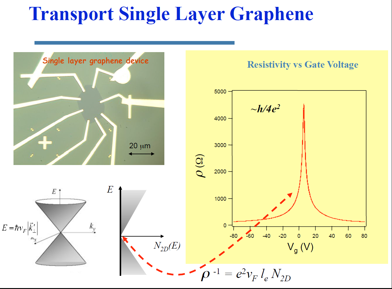
2 Why the interest? 2D crystal with extraordinarily few defects Exotic electrical behaviors E = v F P (massless Dirac fermions) Efficient tunneling through energy barrier, anomalous quantum Hall effects, Excellent materials properties Electrical -- high electron mobility, high current carrying capacity, Mechanical -- large Young s modulus, high tensile strength, low friction, Thermal -- high thermal conductivity Excellent controllability Electrical gating, structural patterning, etc Attractive for fundamental physics and technological applications P x E P y
3 Hot spots of graphene Nobel Prize in Physics for 2010 "for groundbreaking experiments regarding the twodimensional material graphene" Andre Geim Konstantin Novoselov European Commission has chosen graphene as a ten-year, 1 billion euro Future Emerging Technology flagship. (Jan 28, 2013) Aim to get graphene into industry and product development The South Korean government has invested $200 million, beating the amount actually spent on graphene by the UK government so far at least twenty times over. Samsung has added another $200million in South Korean spend.
, 4381 (2010) Ultracapacitor Image: Ron Outlaw Science 329 (5999) 1637 (2010) Graphene Transparent Conductors APL 99, 023111 (2011) and Adv. Mater.")
, 2915 (2010) Nature 467, 190 193 (2010) RF transistors Nano Letters 9 (1), 422 (2009) Nano Letters, 9 (12), 4474 (2009) Science, 327(5966), 662 (2010) IEEE EDL, 31(1), 68 (2010) Nature 467,")
4 Graphene s Applications Flexible Memristors Photo: Sung-Yool Choi Nano Lett., 10 (11), 4381 (2010) Ultracapacitor Image: Ron Outlaw Science 329 (5999) 1637 (2010) Graphene Transparent Conductors APL 99, (2011) and Adv. Mater. 24, 71 (2012) Graphene Photodetector Nature Photonics 4, (2010) Nature Nanotechnology 7, (2012) DNA graphene nanopore Nano Lett., 10 (8), 3163 (2010) Nano Lett.,, 10 (8), 2915 (2010) Nature 467, (2010) RF transistors Nano Letters 9 (1), 422 (2009) Nano Letters, 9 (12), 4474 (2009) Science, 327(5966), 662 (2010) IEEE EDL, 31(1), 68 (2010) Nature 467, (2010) Graphene Commercialization Breakthrough* OLED Lighting Transparent Conductors Logic & Memory Printed Electronics Manufacturing Catalytic support Stretchable and Sensing Electronics Solar Opportunities Energy Storage Advanced carbon based materials for Lithium Ion battery electrodes *
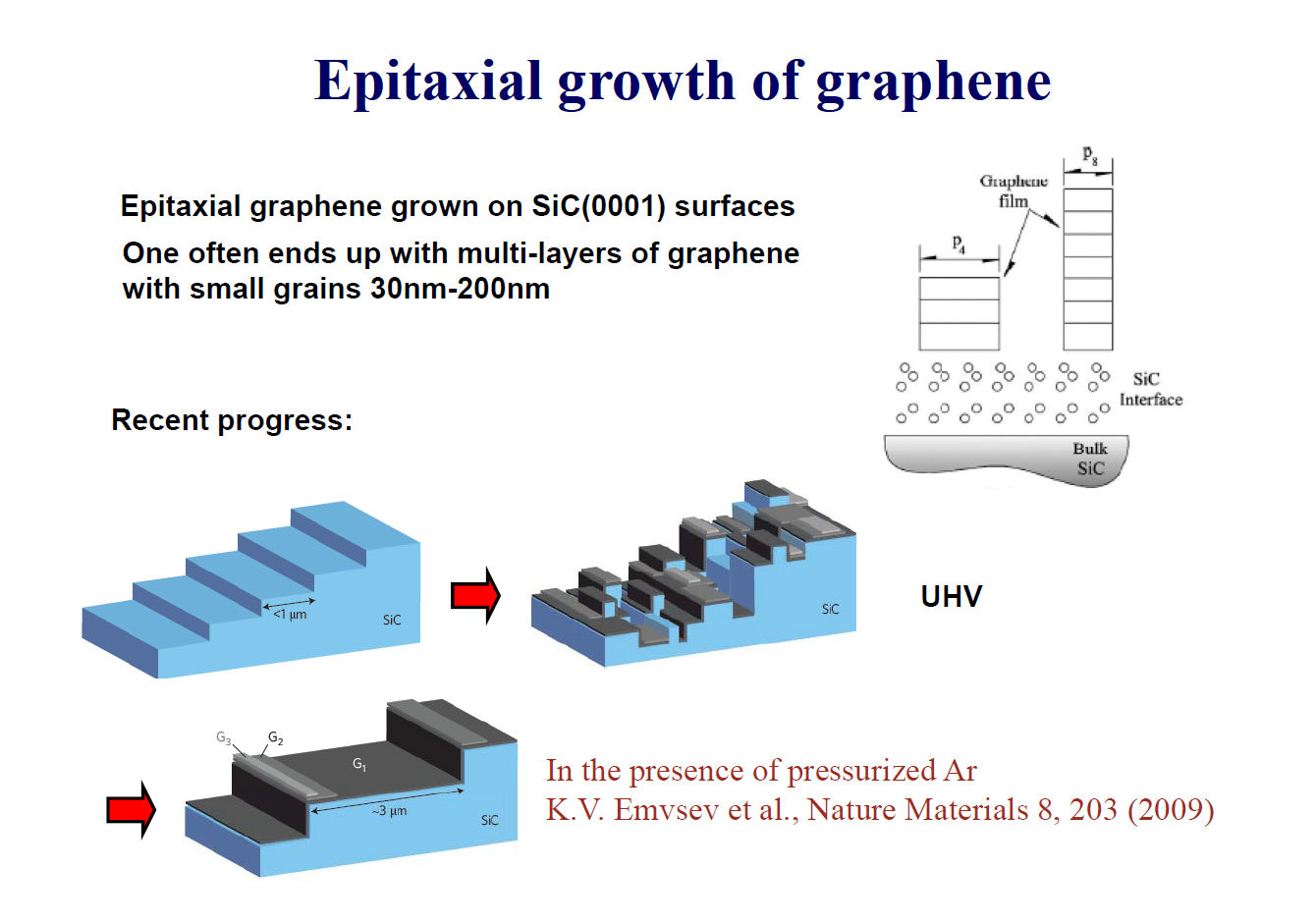
5 Method Descriptions Merits References Mechanical cleavage or exfoliation Chemical oxidized process Epitaxial growth on SiC Fabrication of graphene Scotch Tape Producing GO by the oxidation of graphite with acid Epitaxial growing graphene on SiC Minimal defects Intrinsic properties Small sizes Large scale flakes Composite Large area Multilayer High temperature Science 306, 666 (2004) Nature 442, 282 (2006) J. Phys. Chem. B 108, (2004) Chemical vapor deposition on Ni Ambient-pressure CVD on evaporated polycrystalline Ni Large area multilayer Nano Lett., Vol. 9, No. 1, 200 Chemical vapor deposition on Cu Growing graphene on Cu with methane and hydrogen. Large area, one-layer Defect Mechanism Science 324, 1312 (2009) Solid carbon source to graphene Poly (methyl methacrylate) One step to doped graphene Nature, 468, 549 (2010)


6 Exfoliated Graphene Monolayers and Bilayers Reflecting microscope images. 20 m Monolayer Bilayer K. S. Novoselov et al., Science 306, 666 (2004).
7
8
9 Graphene and Related Carbon sp 2 -bonded Structures Single-layer Bi-layer Fullerenes Nanotubes Nanoribbons
10
11
12
13 STM on Graphene Ripples of graphene on a SiO 2 substrate Atomic resolution Scattering Mechanism? Elena Polyakova et al (Columbia Groups), PNAS (2007) See also Meyer et al, Nature (2007) and Ishigami et al, Nano Letters (2007) Ripples Substrate (charge trap) Absorption Structural defects
14 Unique Properties of Graphene Room-temperature electron mobility of 2.5x10 5 cm 2 V -1 s -1 Nano Lett. 11, (2011). Young s modulus of 1 TPa and intrinsic strength of 130 GPa Cu: TPa Phys. Rev. B 76, (2007). High thermal conductivity: above 3,000Wm -1 K -1 ; Cu: 401Wm -1 K -1 Nature Mater. 10, (2011). Optical absorption of 2.3% No band gap for undoped graphene Science 320, 1308 (2008).
15
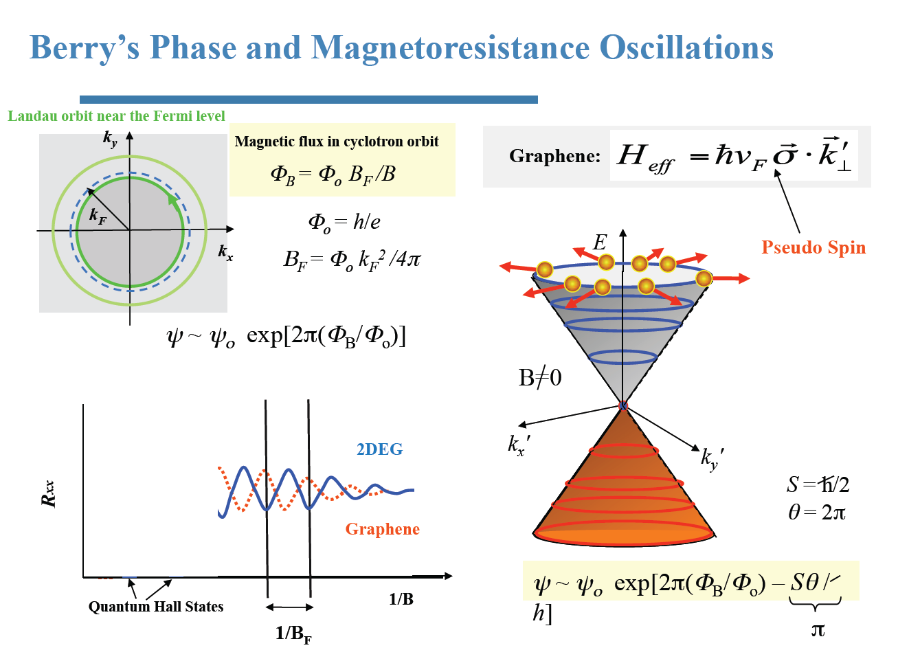
16 Exotic Behaviors -Quantum Hall effect -Barry Phase -Ballistic transport -Klein s paradox -Others..

17 Electron scattering from a potential barrier (1929) As the potential approaches infinity, the reflection diminishes, the electron always transmittes
18 Graphene electronic structures E k relation is linear for low energies near the six corners of the two-dimensional hexagonal Brillouin zone, leading to zero effective mass for electrons and holes. Due to this linear dispersion relation at low energies, electrons and holes near these six points, two of which are inequivalent, behave like relativistic particles described by the Dirac equation for spin 1/2 particles. The electrons and holes are called Dirac fermions, the six corners of the Brillouin zone are called the Dirac points. The equation describing the E k relation is where the Fermi velocity v F ~10 6 m/s.


19 Energy Graphene : 2-D Massless Dirac Fermions Band structure of graphene E hole k x ' k y ' electron k y k x Zero effective mass particles moving with a constant speed v F
20
21

22
23
24
 h -10-15 -50 0 50 V g (V) _1 h_ -6 e 2 _1 h_ -2 e 2 Y. B.")
25 Hll Resistance (k ) Quantum Hall Effect in Graphene T = 3K Novoselov et al ; Zhang et al (2005) _1 h_ 2 e _1 h_ 2 e 2 _1 h_ 6 e _1 h_ 10 e 2 5 _1 h_ 6 e 2 _1 h_ 10 e 2 T = 3K _1 h_ 14 e 2 _1 h_ -14 e _1 h_ -10 e 2 Quantization: -1 _1 _e_ R 2 xy = 4 (n + 2 ) h V g (V) _1 h_ -6 e 2 _1 h_ -2 e 2 Y. B. Zhang et al, Nature 438, 201(2005)

26 R xy (h / 2e 2 ) Room Temperature Quantum Hall Effect K 45 T n (10 12 cm -2 ) Deviation < 0.3% +_ E 1 ~ T Novoselov, Jiang, Zhang, Morozov, Stormer, Zeitler, Maan, Boebinger, Kim, and Geim Science (2007)
 TC145 TC130 n (10 12 cm -2 ) Tan al. PRL (2007)")
27 Graphene Mobility GaAs HEMT Graphene Mobility Modulate Doped GaAs: Pfeiffer et al. TC17 TC12 Mobility (cm 2 /V sec) TC145 TC130 n (10 12 cm -2 ) Tan al. PRL (2007)
28 Toward High Mobility: Suspending Samples graphene SEM image of suspended graphene HF etching -> critical pointing drying AFM image of suspended graphene You should not apply to high gate voltage, otherwise Collapsed graphene devices
29 Graphene Electronics Engineer Dreams Theorist Dreams and more Graphene Veselago lense Cheianov et al. Science (07) Graphene q-bits Trauzettel et al. Nature Phys. (07)


30 The Focusing of Electron Flow and a Veselago Lens in Graphene p-n Junctions Science, VOL 315, 1252 (2007) The focusing of electric current by a single p-n junction in graphene is theoretically predicted, as achieved by fine-tuning the densities of carriers on the n- and p-sides of the junction to equal values. This finding is useful for the engineering of electronic lenses and focused beam splitters using gate-controlled n-p-n junctions in graphene-based transistors.
31 From Graphene Samples To Graphene Devices Contacts: Graphene patterning: Graphene etching: Local gates: PMMA EBL Evaporation HSQ EBL Development Oxygen plasma ALD HfO 2 EBL Evaporation
32 Graphene Nanoribbons: Confined Dirac Particles Gold electrode Graphene Dirac Particle Confinement W W 1 m 10 nm < W < 100 nm Graphene nanoribbon theory partial list W Zigzag ribbons E gap ~ hv F k ~ hv F /W

 10-3 10-4 10-5 30mK 4K 77K 290K -30-20 -10 0 10 20 30 V g (V) 10-5 10-6 10-7 10-8 W = 75 nm 0 20")
33 Conductance ( S) Conductivity ( -1 ) Conductance ( -1 ) Conductance ( -1 ) Conductance ( -1 ) Graphene Ribbon Devices W = 32 nm 10-6 Gold electrode W Graphene Dirac Particle Confinement W E gap ~ hv F / W K 100K 10K 1.7K V g (V) 60 1 m 10 nm < W < 100 nm Wide (> 1 m) Graphene W = 53 nm V g (V) 200K 100K 10K 1.7K 60 V g = 0 V T = 300 K Ribbon Width (nm) mK 4K 77K 290K V g (V) W = 75 nm V g (V) 200K 100K 10K 1.7K 60
34 E g (mev) Scaling of Energy Gaps in Graphene Nanoribbons P1 P2 P3 P4 D1 D W (nm) 90 E g = E 0 /(W-W 0 ) Han, Oezyilmaz, Zhang and Kim PRL (2007)
35
36 Electronic Structure and Pseudospin Physics in Graphene Energy dispersion of the electron in graphene near the Fermi surface looks like that of light, i.e., a cone. E F A pseudospin pointing along k associated with each state, describing the bonding character between the neighboring carbon atoms in the two sublattices. A B The chirality of graphene wavefunctions near the Dirac point suppresses backscattering events. T. Ando, et al (1998); McEuen, Louie, et al (1999)
37 Extremely Long Mean Free Path: Hidden Symmetry? 1D band structure of nanotubes E Low energy band structure of graphene k 1D E F Pseudo spin right moving left moving Small momentum transfer backward scattering becomes inefficient, since it requires pseudo spin flipping. T. Ando, JPSJ (1998); McEuen at al, PRL (1999)
38
 TC17 TC12 TC145 TC130 100 L m (nm) 10 0.01 0.")
39 Conductivity Conductivity, Mobility, & Mean Free Path Mobility Mean free path 100 e 2 /h 1000 TC17 TC12 TC145 TC130 TC17 TC12 TC145 TC130 Mobility (cm 2 /V sec) TC17 TC12 TC145 TC L m (nm) V g (V) n (10 12 cm -2 ) n (10 12 cm -2 )
GRAPHENE: A NEW STAR IN MATERIAL SCIENCE
 GRAPHENE: A NEW STAR IN MATERIAL SCIENCE S. Sahoo 1 & A. K. Dutta 2 Department of Physics, National Institute of Technology Durgapur-713209, West Bengal, India. 1 E-mail: sukadevsahoo@yahoo.com 2 E-mail:
Graphene a material for the future
 Graphene a material for the future by Olav Thorsen What is graphene? What is graphene? Simply put, it is a thin layer of pure carbon What is graphene? Simply put, it is a thin layer of pure carbon It has
Physical Properties and Functionalization of Low-Dimensional Materials
 Physical Properties and Functionalization of Low-Dimensional Materials Physics Department, University of Trieste Graduate School of Physics, XXVI cycle Supervisor: Co-supervisor: Prof. Alessandro BARALDI
Modification of Graphene Films by Laser-Generated High Energy Particles
 Modification of Graphene Films by Laser-Generated High Energy Particles Elena Stolyarova (Polyakova), Ph.D. ATF Program Advisory and ATF Users Meeting April 2-3, 2009, Berkner Hall, Room B, BNL Department
CONTENTS. Preface. 1.1.2. Energy bands of a crystal (intuitive approach)
") CONTENTS Preface. Energy Band Theory.. Electron in a crystal... Two examples of electron behavior... Free electron...2. The particle-in-a-box approach..2. Energy bands of a crystal (intuitive approach)..3.
CONTENTS Preface. Energy Band Theory.. Electron in a crystal... Two examples of electron behavior... Free electron...2. The particle-in-a-box approach..2. Energy bands of a crystal (intuitive approach)..3.
What is Nanophysics: Survey of Course Topics. Branislav K. Nikolić
 What is Nanophysics: Survey of Course Topics Branislav K. Nikolić Department of Physics and Astronomy, University of Delaware, Newark, DE 19716, U.S.A. http://wiki.physics.udel.edu/phys824 Definition of
The Raman Fingerprint of Graphene
 The Raman Fingerprint of Graphene A. C. Ferrari 1, J. C. Meyer 2, V. Scardaci 1, C. Casiraghi 1, M. Lazzeri 3, F. Mauri 3, S. Piscanec 1, D. Jiang 4, K. S. Novoselov 4, S. Roth 2, A. K. Geim 4 1 Department
Solid State Detectors = Semi-Conductor based Detectors
 Solid State Detectors = Semi-Conductor based Detectors Materials and their properties Energy bands and electronic structure Charge transport and conductivity Boundaries: the p-n junction Charge collection
High Open Circuit Voltage of MQW Amorphous Silicon Photovoltaic Structures
 High Open Circuit Voltage of MQW Amorphous Silicon Photovoltaic Structures ARGYRIOS C. VARONIDES Physics and EE Department University of Scranton 800 Linden Street, Scranton PA, 18510 United States Abstract:
Solar Photovoltaic (PV) Cells
 Cells") Solar Photovoltaic (PV) Cells A supplement topic to: Mi ti l S Micro-optical Sensors - A MEMS for electric power generation Science of Silicon PV Cells Scientific base for solar PV electric power generation
Solar Photovoltaic (PV) Cells A supplement topic to: Mi ti l S Micro-optical Sensors - A MEMS for electric power generation Science of Silicon PV Cells Scientific base for solar PV electric power generation
Explain the ionic bonds, covalent bonds and metallic bonds and give one example for each type of bonds.
 Problem 1 Explain the ionic bonds, covalent bonds and metallic bonds and give one example for each type of bonds. Ionic Bonds Two neutral atoms close to each can undergo an ionization process in order
Sub-gap conductance fluctuations in superconductor-graphene hybrid nanostructures
 Sub-gap conductance fluctuations in superconductor-graphene hybrid nanostructures G.Albert, B.Kaviraj, F.Gustavo, F.Lefloch, L.Jansen Laboratoire de Transport Electronique Quantique et Supraconductivité
How To Grow Graphene
 Epitaxial Graphene and Cluster Lattices on Iridium(111) Epitaktisches Graphen und Clustergitter auf Iridium(111) Von der Fakultät für Mathematik, Informatik und Naturwissenschaften der RWTH Aachen University
Graphene and the Quantum Spin Hall Effect
 Graphene and the Quantum Spin Hall Effect Graphene, the Quantum Spin Hall Effect and topological insulators I. Graphene II. Quantum Spin Hall Effect - Spin orbit induced energy gap in graphene A new 2D
Burcu Saner, Firuze Okyay, Fatma Dinç, Neylan Görgülü, Selmiye Alkan Gürsel and Yuda Yürüm*
 Burcu Saner, Firuze Okyay, Fatma Dinç, Neylan Görgülü, Selmiye Alkan Gürsel and Yuda Yürüm* Faculty of Engineering and Natural Sciences, Sabancı University, Istanbul Background about graphene and its separation
Highlights of Solid State Physics. Man of the Year Nobel Prizes
 Highlights of Solid State Physics Man of the Year Nobel Prizes Silicon Technology Moore s Law Gordon Moore Intel Jack Kilby 14 nm 2014 Physics Nobel Prize 2000 Integrated Circuit Electrons in the Conduction
Chapter 5. Second Edition ( 2001 McGraw-Hill) 5.6 Doped GaAs. Solution
 5.6 Doped GaAs. Solution") Chapter 5 5.6 Doped GaAs Consider the GaAs crystal at 300 K. a. Calculate the intrinsic conductivity and resistivity. Second Edition ( 2001 McGraw-Hill) b. In a sample containing only 10 15 cm -3 ionized
Chapter 5 5.6 Doped GaAs Consider the GaAs crystal at 300 K. a. Calculate the intrinsic conductivity and resistivity. Second Edition ( 2001 McGraw-Hill) b. In a sample containing only 10 15 cm -3 ionized
Conductivity of silicon can be changed several orders of magnitude by introducing impurity atoms in silicon crystal lattice.
 CMOS Processing Technology Silicon: a semiconductor with resistance between that of conductor and an insulator. Conductivity of silicon can be changed several orders of magnitude by introducing impurity
Introduction OLEDs OTFTs OPVC Summary. Organic Electronics. Felix Buth. Walter Schottky Institut, TU München. Joint Advanced Student School 2008
 Felix Buth Joint Advanced Student School 2008 Outline 1 Introduction Difference organic/inorganic semiconductors From molecular orbitals to the molecular crystal 2 Organic Light Emitting Diodes Basic Principals
Crystalline solids. A solid crystal consists of different atoms arranged in a periodic structure.
 Crystalline solids A solid crystal consists of different atoms arranged in a periodic structure. Crystals can be formed via various bonding mechanisms: Ionic bonding Covalent bonding Metallic bonding Van
HSMG. There is only one true graphene. www.advancedgrapheneproducts.com
 HSMG TM There is only one true graphene www.advancedgrapheneproducts.com 03. 05. 13. 20. 02 Graphene About AGP About HSMG Collaboration and contact What is graphene Graphene is a flat structure built with
Theoretical investigation on armchair graphene nanoribbons. with oxygen-terminated edges
 Theoretical investigation on armchair graphene nanoribbons with oxygen-terminated edges Hongyu Ge, Guo Wang* and Yi Liao Department of Chemistry, Capital Normal University, Beijing 100048, China * Corresponding
Advanced VLSI Design CMOS Processing Technology
 Isolation of transistors, i.e., their source and drains, from other transistors is needed to reduce electrical interactions between them. For technologies
UNIT I: INTRFERENCE & DIFFRACTION Div. B Div. D Div. F INTRFERENCE
 107002: EngineeringPhysics Teaching Scheme: Lectures: 4 Hrs/week Practicals-2 Hrs./week T.W.-25 marks Examination Scheme: Paper-50 marks (2 hrs) Online -50marks Prerequisite: Basics till 12 th Standard
Lecture 6 Scanning Tunneling Microscopy (STM) General components of STM; Tunneling current; Feedback system; Tip --- the probe.
 General components of STM; Tunneling current; Feedback system; Tip --- the probe.") Lecture 6 Scanning Tunneling Microscopy (STM) General components of STM; Tunneling current; Feedback system; Tip --- the probe. Brief Overview of STM Inventors of STM The Nobel Prize in Physics 1986 Nobel
Lecture 6 Scanning Tunneling Microscopy (STM) General components of STM; Tunneling current; Feedback system; Tip --- the probe. Brief Overview of STM Inventors of STM The Nobel Prize in Physics 1986 Nobel
Le bruit d une impureté Kondo
 Le bruit d une impureté Kondo T. Kontos Laboratoire Pierre Aigrain, Ecole Normale Supérieure, Paris France Experiment:T. Delattre, C. Feuillet-Palma, L.G. Herrmann J.-M. Berroir, B. Plaçais, D.C. Glattli,
JOURNAL INTEGRATED CIRCUITS AND SYSTEMS, VOL 1, NO. 3, JULY 2006. 39
 JOURNAL INTEGRATED CIRCUITS AND SYSTEMS, VOL 1, NO. 3, JULY 2006. 39 Self-Assembled Polystyrene Micro-Spheres Applied for Photonic Crystals and Templates Fabrication Daniel S. Raimundo 1, Francisco J.
Nanoelectronics 09. Atsufumi Hirohata Department of Electronics. Quick Review over the Last Lecture
 Nanoelectronics 09 Atsufumi Hirohata Department of Electronics 12:00 Wednesday, 4/February/2015 (P/L 006) Quick Review over the Last Lecture ( Field effect transistor (FET) ): ( Drain ) current increases
Solid-State Physics: The Theory of Semiconductors (Ch. 10.6-10.8) SteveSekula, 30 March 2010 (created 29 March 2010)
 SteveSekula, 30 March 2010 (created 29 March 2010)") Modern Physics (PHY 3305) Lecture Notes Modern Physics (PHY 3305) Lecture Notes Solid-State Physics: The Theory of Semiconductors (Ch. 10.6-10.8) SteveSekula, 30 March 2010 (created 29 March 2010) Review
Modern Physics (PHY 3305) Lecture Notes Modern Physics (PHY 3305) Lecture Notes Solid-State Physics: The Theory of Semiconductors (Ch. 10.6-10.8) SteveSekula, 30 March 2010 (created 29 March 2010) Review
TRANSPORT PROPERTIES OF GRAPHENE IN AND OUT OF THE BULK
 TRANSPORT PROPERTIES OF GRAPHENE IN AND OUT OF THE BULK Jean-Paul Issi Université de Louvain Louvain-la-Neuve Graphene International School, Cargese, October, 2010 PART I ELECTRICAL CONDUCTIVITY PART II
Semiconductors, diodes, transistors
 Semiconductors, diodes, transistors (Horst Wahl, QuarkNet presentation, June 2001) Electrical conductivity! Energy bands in solids! Band structure and conductivity Semiconductors! Intrinsic semiconductors!
Material Requirements For 3D IC and Packaging Presented by: W. R. Bottoms
 Material Requirements For 3D IC and Packaging Presented by: W. R. Bottoms Frontiers of Characterization and Metrology for Nanoelectronics Hilton Dresden April 14-16, 2015 Industry Needs Are Changing Moore
The influence of graphene curvature on hydrogen adsorption. Sarah Goler
 The influence of graphene curvature on hydrogen adsorption Sarah Goler Laboratorio NEST, Istituto Nanoscienze CNR and Scuola Normale Superiore, Piazza San Silvestro 12, 56127 Pisa, Italy Center for Nanotechnology
MOS (metal-oxidesemiconductor) 李 2003/12/19
 李 2003/12/19") MOS (metal-oxidesemiconductor) 李 2003/12/19 Outline Structure Ideal MOS The surface depletion region Ideal MOS curves The SiO 2 -Si MOS diode (real case) Structure A basic MOS consisting of three layers.
MOS (metal-oxidesemiconductor) 李 2003/12/19 Outline Structure Ideal MOS The surface depletion region Ideal MOS curves The SiO 2 -Si MOS diode (real case) Structure A basic MOS consisting of three layers.
Introduction to VLSI Fabrication Technologies. Emanuele Baravelli
 Introduction to VLSI Fabrication Technologies Emanuele Baravelli 27/09/2005 Organization Materials Used in VLSI Fabrication VLSI Fabrication Technologies Overview of Fabrication Methods Device simulation
Nanotechnologies for the Integrated Circuits
 Nanotechnologies for the Integrated Circuits September 23, 2015 Dr. Bertrand Cambou Professor of Practice NAU, Cybersecurity School of Informatics, Computing, and Cyber-Systems Agenda The Market Silicon
Nanometer-scale imaging and metrology, nano-fabrication with the Orion Helium Ion Microscope
 andras@nist.gov Nanometer-scale imaging and metrology, nano-fabrication with the Orion Helium Ion Microscope Bin Ming, András E. Vladár and Michael T. Postek National Institute of Standards and Technology
Spatially separated excitons in 2D and 1D
 Spatially separated excitons in 2D and 1D David Abergel March 10th, 2015 D.S.L. Abergel 3/10/15 1 / 24 Outline 1 Introduction 2 Spatially separated excitons in 2D The role of disorder 3 Spatially separated
fotoelektron-spektroszkópia Rakyta Péter
 Spin-pálya kölcsönhatás grafénben, fotoelektron-spektroszkópia Rakyta Péter EÖTVÖS LORÁND TUDOMÁNYEGYETEM, KOMPLEX RENDSZEREK FIZIKÁJA TANSZÉK 1 Introduction to graphene Sp 2 hybridization p z orbitals
Matter, Materials, Crystal Structure and Bonding. Chris J. Pickard
 Matter, Materials, Crystal Structure and Bonding Chris J. Pickard Why should a theorist care? Where the atoms are determines what they do Where the atoms can be determines what we can do Overview of Structure
Total Organic Synthesis and Characterization of Graphene Nanoribbons
 Total Organic Synthesis and Characterization of Graphene Nanoribbons Gang Li Seminar in Dong group 03/26/2014 Content History of Graphene Synthesis and Characterization and Properties of Graphene Conceptual
STUDY OF FIELD EFFECT TRANSISTORS BASED ON LAYERED SEMICONDUCTORS: GRAPHENE AND BEYOND. A Dissertation. Presented to
 STUDY OF FIELD EFFECT TRANSISTORS BASED ON LAYERED SEMICONDUCTORS: GRAPHENE AND BEYOND A Dissertation Presented to the Faculty of the Department of Physics University of Houston In Partial Fulfillment
Nanocomputer & Architecture
 Nanocomputer & Architecture Yingjie Wei Western Michigan University Department of Computer Science CS 603 - Dr. Elise dedonckor Febrary 4 th, 2004 Nanocomputer Architecture Contents Overview of Nanotechnology
 g 0 = 3 ev Linear a = 0.246nm. constant velocity g 0 ~ 3 ev 0.334nm Interlayer g 1 ~ 0.4 ev Massive Effective mass: Graphene monolayer-bilayer junction Theoretical studies Nakanishi, Koshino, Ando, PRB
The Physics of Energy sources Renewable sources of energy. Solar Energy
 The Physics of Energy sources Renewable sources of energy Solar Energy B. Maffei Bruno.maffei@manchester.ac.uk Renewable sources 1 Solar power! There are basically two ways of using directly the radiative
Lara Lama laral@kth.se. Axel Nordström axenor@kth.se. Supervisors: Jan Linnros Ilya Sychugov
 Photoluminescence and AFM characterization of silicon nanocrystals prepared by low-temperature plasma enhanced chemical vapour deposition and annealing Lara Lama laral@kth.se Axel Nordström axenor@kth.se
CS257 Introduction to Nanocomputing
 CS257 Introduction to Nanocomputing Overview of Crossbar-Based Computing John E Savage Overview Intro to NW growth methods Chemical vapor deposition and fluidic assembly Nano imprinting Nano stamping Four
Implementation Of High-k/Metal Gates In High-Volume Manufacturing
 White Paper Implementation Of High-k/Metal Gates In High-Volume Manufacturing INTRODUCTION There have been significant breakthroughs in IC technology in the past decade. The upper interconnect layers of
Semiconductor doping. Si solar Cell
 Semiconductor doping Si solar Cell Two Levels of Masks - photoresist, alignment Etch and oxidation to isolate thermal oxide, deposited oxide, wet etching, dry etching, isolation schemes Doping - diffusion/ion
BROADBAND PHOTOCURRENT ENHANCEMENT IN LONGWAVE INFRARED QUANTUM DOT PHOTODETECTORS BY SUB-WAVELENGTH SURFACE GRATINGS
 Optics and Photonics Letters Vol. 6, No. 1 (2013) 1350002 (6 pages) c World Scientific Publishing Company DOI: 10.1142/S1793528813500020 BROADBAND PHOTOCURRENT ENHANCEMENT IN LONGWAVE INFRARED QUANTUM
Defect Engineering in Semiconductors
 Defect Engineering in Semiconductors Silicon Technology: problems of ultra large-scale l integration i Gettering in silicon Defect engineering in HgCdTe Near-surface defects in GaAs after diamond saw-cutting
CVD SILICON CARBIDE. CVD SILICON CARBIDE s attributes include:
 CVD SILICON CARBIDE CVD SILICON CARBIDE is the ideal performance material for design engineers. It outperforms conventional forms of silicon carbide, as well as other ceramics, quartz, and metals in chemical
Focused Ion beam nanopatterning: potential application in photovoltaics
 Focused Ion beam nanopatterning: potential application in photovoltaics Research Infrastructure: Location: FIB-Focused Ion Beam ENEA Portici (Italy) Date March, 26 2013 Speakers: Vera La Ferrara, ENEA
Experimental Observation of the Quantum Anomalous Hall Effect in a Magnetic Topological Insulator
 Experimental Observation of the Quantum Anomalous Hall Effect in a Magnetic Topological Insulator Chang et al., Science 340, 167 (2013). Joseph Hlevyack, Hu Jin, Mazin Khader, Edward Kim Outline: Introduction:
Exciton dissociation in solar cells:
 Exciton dissociation in solar cells: Xiaoyang Zhu Department of Chemistry University of Minnesota, Minneapolis t (fs) 3h! E, k h! Pc Bi e - 1 Acknowledgement Organic semiconductors: Mutthias Muntwiler,
Phonon Scattering and Thermal Conduction in Nanostructured Semiconductors
 Phonon Scattering and Thermal Conduction in Nanostructured Semiconductors David G. Cahill, Joe Feser, Yee Kan Koh Department of Materials Science and Engineering And Materials Research Laboratory University
Supporting information
 Supporting information Ultrafast room-temperature NH 3 sensing with positively-gated reduced graphene oxide field-effect transistors Ganhua Lu 1, Kehan Yu 1, Leonidas E. Ocola 2, and Junhong Chen 1 * 1
Introduction to the Physical Properties of Graphene. Lecture Notes 2008
 Introduction to the Physical Properties of Graphene Jean-Noël FUCHS Mark Oliver GOERBIG Lecture Notes 2008 ii Contents 1 Introduction to Carbon Materials 1 1.1 The Carbon Atom and its Hybridisations............
h e l p s y o u C O N T R O L
 contamination analysis for compound semiconductors ANALYTICAL SERVICES B u r i e d d e f e c t s, E v a n s A n a l y t i c a l g r o u p h e l p s y o u C O N T R O L C O N T A M I N A T I O N Contamination
Novel inkjettable copper ink utilizing processing temperatures under 100 degrees C without the need of inert atmosphere
 Novel inkjettable copper ink utilizing processing temperatures under 100 degrees C without the need of inert atmosphere Printed Electronics Europe April 7-8, 2009 Dresden, Germany Dr. Zvi Yaniv Applied
POLYMER BASED PHOTOVOLTAICS
 PLYMER BASED PHTVLTAICS Novel concepts, materials and state-of-the-art performances Jan Kroon Semiconducting polymers Nobel Prize Chemistry 2000 (Alan J. Heeger, Alan G. MacDiarmid, Hideki Shirakawa) Conducting
Università degli Studi di Padova Dipartimento di Fisica e Astronomia Corso di Laurea Magistrale in Fisica
 Università degli Studi di Padova Dipartimento di Fisica e Astronomia Corso di Laurea Magistrale in Fisica SCANNING PROBE MICROSCOPY OF GRAPHENE AND SELF-ASSEMBLED MOLECULES Nicola Galvanetto ANNO ACCADEMICO
Types of Epitaxy. Homoepitaxy. Heteroepitaxy
 Epitaxy Epitaxial Growth Epitaxy means the growth of a single crystal film on top of a crystalline substrate. For most thin film applications (hard and soft coatings, optical coatings, protective coatings)
FYS3410 - Vår 2014 (Kondenserte fasers fysikk) http://www.uio.no/studier/emner/matnat/fys/fys3410/v14/index.html
 http://www.uio.no/studier/emner/matnat/fys/fys3410/v14/index.html") FYS3410 - Vår 2014 (Kondenserte fasers fysikk) http://www.uio.no/studier/emner/matnat/fys/fys3410/v14/index.html Pensum: Solid State Physics by Philip Hofmann (Chapters 1-7 and 11) Andrej Kuznetsov delivery
FYS3410 - Vår 2014 (Kondenserte fasers fysikk) http://www.uio.no/studier/emner/matnat/fys/fys3410/v14/index.html Pensum: Solid State Physics by Philip Hofmann (Chapters 1-7 and 11) Andrej Kuznetsov delivery
Contents of Technology Course
 Contents of Technology Course General observations: The material is organized in modules. Each module treats a distinct part of device fabrication. There is also an introduction (Module 1), a part that
Solar Energy. Outline. Solar radiation. What is light?-- Electromagnetic Radiation. Light - Electromagnetic wave spectrum. Electromagnetic Radiation
 Outline MAE 493R/593V- Renewable Energy Devices Solar Energy Electromagnetic wave Solar spectrum Solar global radiation Solar thermal energy Solar thermal collectors Solar thermal power plants Photovoltaics
SUPERCONDUCTIVITY. PH 318- Introduction to superconductors 1
 SUPERCONDUCTIVITY property of complete disappearance of electrical resistance in solids when they are cooled below a characteristic temperature. This temperature is called transition temperature or critical
Graduate Student Presentations
 Graduate Student Presentations Dang, Huong Chip packaging March 27 Call, Nathan Thin film transistors/ liquid crystal displays April 4 Feldman, Ari Optical computing April 11 Guerassio, Ian Self-assembly
Chemical vapor deposition of novel carbon materials
 Thin Solid Films 368 (2000) 193±197 www.elsevier.com/locate/tsf Chemical vapor deposition of novel carbon materials L. Chow a, b, *, D. Zhou b, c, A. Hussain b, c, S. Kleckley a, K. Zollinger a, A. Schulte
Picosun World Forum, Espoo 9.6.2009. 35 years of ALD. Tuomo Suntola, Picosun Oy. Tuomo Suntola, Picosun Oy
 35 years of ALD Conventional methods for compound film deposition Heat treatment Final crystallization Nucleation Vacuum evaporation Sputtering CVD Buildup of thin film in source controlled deposition
Quantum Computing for Beginners: Building Qubits
 Quantum Computing for Beginners: Building Qubits Suzanne Gildert Condensed Matter Physics Research (Quantum Devices Group) University of Birmingham 28/03/2007 Overview of this presentation What is a Qubit?
Graphene-based Composite Thin Films for Electronics
 Graphene-based Composite Thin Films for Electronics NANO LETTERS 2009 Vol. 9, No. 2 814-818 Goki Eda and Manish Chhowalla* Rutgers UniVersity, Materials Science and Engineering, Piscataway, New Jersey
ELEC 3908, Physical Electronics, Lecture 15. BJT Structure and Fabrication
 ELEC 3908, Physical Electronics, Lecture 15 Lecture Outline Now move on to bipolar junction transistor (BJT) Strategy for next few lectures similar to diode: structure and processing, basic operation,
FYS3410 - Vår 2015 (Kondenserte fasers fysikk) http://www.uio.no/studier/emner/matnat/fys/fys3410/v15/index.html
 http://www.uio.no/studier/emner/matnat/fys/fys3410/v15/index.html") FYS3410 - Vår 015 (Kondenserte fasers fysikk) http://www.uio.no/studier/emner/matnat/fys/fys3410/v15/index.html Pensum: Introduction to Solid State Physics by Charles Kittel (Chapters 1-9 and 17, 18, 0,
FYS3410 - Vår 015 (Kondenserte fasers fysikk) http://www.uio.no/studier/emner/matnat/fys/fys3410/v15/index.html Pensum: Introduction to Solid State Physics by Charles Kittel (Chapters 1-9 and 17, 18, 0,
Tobias Märkl. November 16, 2009
 ,, Tobias Märkl to 1/f November 16, 2009 1 / 33 Content 1 duction to of Statistical Comparison to Other Types of Noise of of 2 Random duction to Random General of, to 1/f 3 4 2 / 33 , to 1/f 3 / 33 What
Thermal unobtainiums? The perfect thermal conductor and the perfect thermal insulator
 Thermal unobtainiums? The perfect thermal conductor and the perfect thermal insulator David G. Cahill Materials Research Lab and Department of Materials Science and Engineering, U. of Illinois Gratefully
Coating Technology: Evaporation Vs Sputtering
 Satisloh Italy S.r.l. Coating Technology: Evaporation Vs Sputtering Gianni Monaco, PhD R&D project manager, Satisloh Italy 04.04.2016 V1 The aim of this document is to provide basic technical information
Chemical Synthesis. Overview. Chemical Synthesis of Nanocrystals. Self-Assembly of Nanocrystals. Example: Cu 146 Se 73 (PPh 3 ) 30
 30") Chemical Synthesis Spontaneous organization of molecules into stable, structurally well-defined aggregates at the nanometer length scale. Overview The 1-100 nm nanoscale length is in between traditional
Chemical Synthesis Spontaneous organization of molecules into stable, structurally well-defined aggregates at the nanometer length scale. Overview The 1-100 nm nanoscale length is in between traditional
ELG4126: Photovoltaic Materials. Based Partially on Renewable and Efficient Electric Power System, Gilbert M. Masters, Wiely
 ELG4126: Photovoltaic Materials Based Partially on Renewable and Efficient Electric Power System, Gilbert M. Masters, Wiely Introduction A material or device that is capable of converting the energy contained
Lecture 14. Introduction to the Sun
 Lecture 14 Introduction to the Sun ALMA discovers planets forming in a protoplanetary disc. Open Q: what physics do we learn about the Sun? 1. Energy - nuclear energy - magnetic energy 2. Radiation - continuum
FUNDAMENTAL PROPERTIES OF SOLAR CELLS
 FUNDAMENTAL PROPERTIES OF SOLAR CELLS January 31, 2012 The University of Toledo, Department of Physics and Astronomy SSARE, PVIC Principles and Varieties of Solar Energy (PHYS 4400) and Fundamentals of
Optical Hyperdoping: Transforming Semiconductor Band Structure for Solar Energy Harvesting
 Optical Hyperdoping: Transforming Semiconductor Band Structure for Solar Energy Harvesting 3G Solar Technologies Multidisciplinary Workshop MRS Spring Meeting San Francisco, CA, 5 April 2010 Michael P.
Carbon-Carbon bonds: Hybridization
 Carbon-Carbon bonds: Hybridization Abstract: Gina 05/05/11 Molecular binding behavior has a large inuence on the structure of a material and their properties. As a exclusion, carbon bind themself not in
CONCEPT OF DETERMINISTIC ION IMPLANTATION AT THE NANOSCALE
 CONCEPT OF DETERMINISTIC ION IMPLANTATION AT THE NANOSCALE Daniel Spemann Jan Meijer 1, Jürgen W. Gerlach, Paul Räcke 1, Susann Liedtke, Stephan Rauschenbach 2, Bernd Rauschenbach 1 University of Leipzig,
Solar Cell Parameters and Equivalent Circuit
 9 Solar Cell Parameters and Equivalent Circuit 9.1 External solar cell parameters The main parameters that are used to characterise the performance of solar cells are the peak power P max, the short-circuit
Lecture 12. Physical Vapor Deposition: Evaporation and Sputtering Reading: Chapter 12. ECE 6450 - Dr. Alan Doolittle
 Lecture 12 Physical Vapor Deposition: Evaporation and Sputtering Reading: Chapter 12 Evaporation and Sputtering (Metalization) Evaporation For all devices, there is a need to go from semiconductor to metal.
GREEN NANOTECHNOLOGY. Geoffrey. Energy in the Built Environment. Solutions for Sustainability and. B. Smith Claes G. Granqvist.
 GREEN NANOTECHNOLOGY Solutions for Sustainability and Energy in the Built Environment Geoffrey B. Smith Claes G. Granqvist CRC Press Taylor & Francis Group Boca Raton London NewYork CRC Press is an imprint
Demonstration of sub-4 nm nanoimprint lithography using a template fabricated by helium ion beam lithography
 Demonstration of sub-4 nm nanoimprint lithography using a template fabricated by helium ion beam lithography Wen-Di Li*, Wei Wu** and R. Stanley Williams Hewlett-Packard Labs *Current address: University
OPTIMIZING OF THERMAL EVAPORATION PROCESS COMPARED TO MAGNETRON SPUTTERING FOR FABRICATION OF TITANIA QUANTUM DOTS
 OPTIMIZING OF THERMAL EVAPORATION PROCESS COMPARED TO MAGNETRON SPUTTERING FOR FABRICATION OF TITANIA QUANTUM DOTS Vojtěch SVATOŠ 1, Jana DRBOHLAVOVÁ 1, Marian MÁRIK 1, Jan PEKÁREK 1, Jana CHOMOCKÁ 1,
Vacuum Evaporation Recap
 Sputtering Vacuum Evaporation Recap Use high temperatures at high vacuum to evaporate (eject) atoms or molecules off a material surface. Use ballistic flow to transport them to a substrate and deposit.
CARBON NANOTUBE NANOELECTROMECHANICAL SYSTEMS
 CARBON NANOTUBE NANOELECTROMECHANICAL SYSTEMS PHD THESIS BY MARIANNA SLEDZINSKA Director: Prof. Adrian Bachtold Tutor de la UAB: Prof. Javier Rodriguez Dr. Adrian Bachtold, profesor del CSIC en el CIN2,
New materials on horizon for advanced logic technology in mobile era
 New materials on horizon for advanced logic technology in mobile era source gate Kelin J. Kuhn, TED 2012 drain Franz Kreupl, IFX 2003 Hsinchu March 6, 2013 - Prof. Dr. Franz Kreupl 1 Outline Introduction
Photovoltaics photo volt Photovoltaic Cells Crystalline Silicon Cells Photovoltaic Systems
 1 Photovoltaics Photovoltaic (PV) materials and devices convert sunlight into electrical energy, and PV cells are commonly known as solar cells. Photovoltaics can literally be translated as light-electricity.
An organic semiconductor is an organic compound that possesses similar
 MSE 542 Final Term Paper Title: Organic Semiconductor for Flexible Electronics Name: Chunhung Huang Introduction: An organic semiconductor is an organic compound that possesses similar properties to inorganic
Scanning Near Field Optical Microscopy: Principle, Instrumentation and Applications
 Scanning Near Field Optical Microscopy: Principle, Instrumentation and Applications Saulius Marcinkevičius Optics, ICT, KTH 1 Outline Optical near field. Principle of scanning near field optical microscope
Free Electron Fermi Gas (Kittel Ch. 6)
") Free Electron Fermi Gas (Kittel Ch. 6) Role of Electrons in Solids Electrons are responsible for binding of crystals -- they are the glue that hold the nuclei together Types of binding (see next slide)
Free Electron Fermi Gas (Kittel Ch. 6) Role of Electrons in Solids Electrons are responsible for binding of crystals -- they are the glue that hold the nuclei together Types of binding (see next slide)
SYNOPSIS OF DEVELOPMENT OF GRAPHENE AND SILICON NANOWIRES FOR PHOTOVOLTAIC AND FIELD ELECTRON EMISSION APPLICATIONS
 SYNOPSIS OF DEVELOPMENT OF GRAPHENE AND SILICON NANOWIRES FOR PHOTOVOLTAIC AND FIELD ELECTRON EMISSION APPLICATIONS A Thesis to be submitted by SANJAY KUMAR BEHURA (Roll Number: 09SSEPH06) For the Award
ELECTRICAL CONDUCTION
 Chapter 12: Electrical Properties Learning Objectives... How are electrical conductance and resistance characterized? What are the physical phenomena that distinguish conductors, semiconductors, and insulators?
Contents. Goldstone Bosons in 3He-A Soft Modes Dynamics and Lie Algebra of Group G:
 ... Vlll Contents 3. Textures and Supercurrents in Superfluid Phases of 3He 3.1. Textures, Gradient Energy and Rigidity 3.2. Why Superfuids are Superfluid 3.3. Superfluidity and Response to a Transverse
From Nano-Electronics and Photonics to Renewable Energy
 From Nano-Electronics and Photonics to Renewable Energy Tom Smy Department of Electronics, Carleton University Questions are welcome! OUTLINE Introduction: to EE and Engineering Physics Renewable Energy