The Raman Fingerprint of Graphene
|
|
|
- Peregrine Bridges
- 7 years ago
- Views:
Transcription
1 The Raman Fingerprint of Graphene A. C. Ferrari 1, J. C. Meyer 2, V. Scardaci 1, C. Casiraghi 1, M. Lazzeri 3, F. Mauri 3, S. Piscanec 1, D. Jiang 4, K. S. Novoselov 4, S. Roth 2, A. K. Geim 4 1 Department of Engineering, University of Cambridge, Cambridge, UK 2 Max Planck Institute for Solid State Research, Stuttgart 70569, Germany 3 Institut de Mineralogie et de Physique des Milieux Condenses, Paris, France 4 Department of Physics and Astronomy, University of Manchester, UK

2 NanoTube-Evolution-Nagano 06

3 NanoTube-Evolution-Nagano 06 Cut. Get graphene Eklund-Sensei NT06 Press (50GPa) Get Diamond-like Carbon! S. Saito-Sensei CCNT06

4 Graphene.big hype recently Electron transport described by the (relativistic-like) Dirac equation Access to the rich and subtle physics of quantum electrodynamics in a relatively simple condensed matter experiment Scalability of graphene devices to true nanometre dimensions makes it a promising candidate for future electronic applications, because of its ballistic transport at room temperature combined with chemical and mechanical stability. Graphene is the two-dimensional (2d) building block for carbon allotropes of every other dimensionality

5 Transistor: Graphene Ribbon

6 How to Make Graphene? Drawing: (micro) mechanical cleavage of graphite

7 How to Make Graphene? GRAPHITE IS STRONGLY LAYERED SLICE DOWN TO ONE ATOMIC PLANE individual atomic sheets: do they exist?

8 Free-Standing Graphene 0Å 9Å 13Å AFM Key: Visual Identification 1 μm SEM OPTICS 1 μm single layer of atoms visible by naked eye only on 300 nm SiO 2 1 μm

9 However Need Extremely Good Eye To Spot!!! Single Layer

10 Two Layers

11 One Comment Mechanical cleavage is nice and simple However Low yield, messy, not scalable Better to grow graphene directly on substrate This can be done But not the subject of this talk

12 Another Comment AFM thickness of single layer is nm! Due to chemical contrast We want to be 150% sure TEM

13 Free-Hanging graphene sheets J. C. Meyer 500nm 1 layer of graphene!

14 Preparation 1. Graphene sheet on substrate 2. Metal grid patterned onto the flake 2µm 10µm

15 Preparation 3. Etching of substrate 4. TEM and electron diffraction analysis 500nm 10µm Flake remains DEPARTMENT in metal OF grid ENGINEERING

16 Electron diffraction: Highly crystalline samples Number of layers? Diffraction tilt series!

17 One-layer graphene Sheets fold back at the edges, and sometimes show a wrinkle within the sheet. HRTEM analysis of the folding allows to verify the layer count. 2nm 2nm

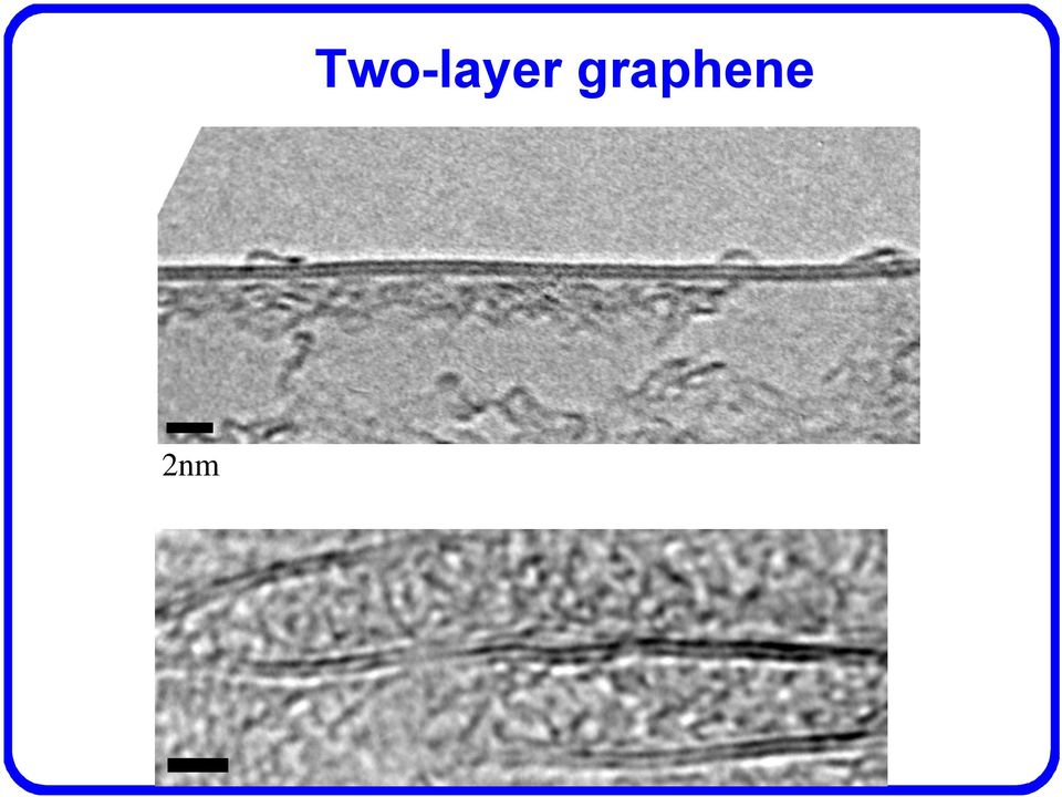
18 Two-layer graphene 2nm
19 Two-Layer Graphene 2 Layers Stacking A/B

20 8 layers

21 We Need High Throughput Non Destructive Quick Substrate Independent Identification Technique Raman Spectroscopy
22 514nm Intensity Graphene Graphite Raman shift (cm -1 )
23 nm Intensity (a. u.) Graphite Graphene G Peak (2D peak) Clear Fingerprint Raman shift (cm-1)
24 Graphene Intensity (A.U.) Intensity (A.U.) Raman Shift (cm -1 ) Raman Shift (cm -1 )
25 Graphene Intensity (A.U.) D peak intensity NOT related to Number of Layers Disorder (in the widest possible meaning) Intensity (A.U.) See Tuinstra Koening Raman Shift (cm -1 ) Raman Shift (cm -1 )
26 Graphene Intensity (A.U.) On Substrate Suspended Raman Shift (cm -1 )
27 514 nm 2-Layers Intensity (A.U.) Intensity (A.U.) Raman Shift (cm -1 ) Raman Shift (cm -1 )
28 514nm 633 nm graphite Intensity (a. u.) 10 layers 5 layers 2 layers Raman shift (cm -1 ) 1 layer Slight Upshift ~ 5cm -1 Raman shift (cm -1 )
29 514nm 633 nm graphite Intensity (a. u.) 10 layers 5 layers 2 layers Raman shift (cm -1 ) 1 layer Raman shift (cm -1 )
30 2500 D) nm Edge Graphite E) 2 Layer 2D 1B 2D 1A 2D 2A 2D 2B Intensity (A. U.) D1 D2 Intensity (A.U.) nm 500 Edge 1 Layer nm D Raman Shift (cm -1 ) Raman Shift (cm -1 )
31 The Origin of G (2D) Peak Named G since is one of the 2 biggest peaks in graphite BUT it is the second order of D peak Nothing to do with G peak D forbidden in perfect crystal By Raman Fundamental Selection Rule q~0 However 2 nd order always allowed: q+(-q)=0
32 D Peak Dispersion Pocsik et al. (1998) Vidano et al. (1981)
33 D peak comes from LO phonons (Ferrari Robertson 2000) Active by double resonance (Baranov 1988, Thomsen-Reich 2000) Strongly dispersive due to Kohn Anomaly at K (Piscanec et al. 2004)
34 However Second order no defect scattering necessary In principle ALL phonons active BUT Double resonant phonons enhanced due to resonance and strong electron-phonon coupling
35 Previous double resonance models predict multiple D peaks for graphene in contrast with experiments Double structure of 2D peak in graphite never explained Traditional interpretation (1980) 2 Maxima in graphite Phonon Density of States at K and M WRONG since 2D disperses with excitation KEY: Evolution of Electron Bands with number of layers
36 Three Possible Processes However: only 1 contributes
37 OK! Small: Trigonal Warping Three Possible Processes Forbidden: EPC=0 However: only 1 contributes
38 Trigonal Warping Effect q > K Strong EPC and large portion of the phase-space q < K Strong EPC but small portion of the phase-space q ~ K EPC~0 Adapted from: Kurti et al., Phys. Rev. B (2002)
39 1 Component D and 2D peaks nm D 514 nm 2D Intensity (A. U.) Edge 1 Layer Intensity (a. u.) Graphene Raman Shift (cm -1 ) Raman shift (cm-1 )
40 Two possibilities: 1) Phonon Splitting Two-layer Graphene 2) Band splitting Phonon Splitting K-M is Minor Μ Κ Γ q = (ξ,0,0) 1300 PRL 93, (2004) ve Vector (2π/a 0 )
41 Band Splitting Main Effect Layer 2D 1B 2D 1A 2D 2A 2D 2B Intensity (A.U.) nm nm Raman Shift (cm -1 ) 4 components 2 Most intense
42 Origin of Small Upshift of G peak ~5 cm -1 Upshift graphite Intensity (a. u.) 1 layer R am an shift (cm -1 ) IR Raman Graphene Raman Graphite PRL 93, (2004) q = (0,ξ,0) Γ Kohn Anomaly
43 Phonon-Linewidths and EPC In a perfect crystal, phonon linewidths determined by Interaction with other elementary excitations: an γ = γ + γ EPC γ an : anharmonic contribution, due to interaction With other phonons. Determined by anharmonic terms in interatomic potential. γ EPC : interaction with electron-hole pairs. Determined by EPC and present in systems with null electron gap
44 Γ-E 2g LO Phonon Decay Processes From the Fermi Golden Rule: γ EPC Γ EPC( Γ E2 LO g β 2 2 )
45 Intensity (A. U.) Γ-E 2g LO : Graphite Raman G Peak Single Crystal Graphite FWHM(G)= 13.5 cm Raman DEPARTMENT Shift (cm OF -1 ENGINEERING ) No D Peak No extra broadening due to disorder No FWHM(G) increase with temperature γ an 1.5 cm -1 (spectrometer resolution) EPC(Γ)=45.5 (ev/ą) 2
46 And Single layer graphene Intensity (A.U.) FWHM(G)= 14 cm -1 Similar EPC PRB 73, (2006) Raman Shift (cm -1 )
47 Implications for Nanotubes Single 2D peak graphene Single 2D peak in Single Wall CNT Curvature and confinement give diameter dependence 2D(SWNT)~2D (graphene)- A/d 2D position in Graphite should not be used to scale Distribution of SWNTs of different diameters, DEPARTMENT distribution OF ENGINEERING of 2D AND peaks MATERIALS GROUP
48 What about Multi-Wall? First approximation each wall gives a 2D peak DWNT two 2D peaks (inner and outer wall) HOWEVER, inter-wall interactions Can change simple picture Further splitting, Less peaks! Details to follow
49 Conclusions Identified unique features of Raman spectrum, which fingerprints graphene amongst all other carbon allotropes. The Raman spectrum evolution with increasing number of layers reflects the evolution of the electronic structure and electron-phonon interactions Raman spectroscopy is a quick, high-throughput, non-destructive technique for the unambiguous identification of graphene layers. Raman+Graphene is Good Fun!
50 Funding: CPU: EU FAMOUS & CANAPE project Marie Curie Fellowship IHP-HPMT-CT The Royal Society EPSRC GR/S97620/01 The Leverhulme Trust HPCF, Cambridge UK IDRIS, Orsay France
51 Reference
Raman and AFM characterization of carbon nanotube polymer composites Illia Dobryden
 Raman and AFM characterization of carbon nanotube polymer composites Illia Dobryden This project is conducted in High Pressure Spectroscopy Laboratory (Materials Physics group) Supervisor: Professor Alexander
Graphene a material for the future
 Graphene a material for the future by Olav Thorsen What is graphene? What is graphene? Simply put, it is a thin layer of pure carbon What is graphene? Simply put, it is a thin layer of pure carbon It has
Burcu Saner, Firuze Okyay, Fatma Dinç, Neylan Görgülü, Selmiye Alkan Gürsel and Yuda Yürüm*
 Burcu Saner, Firuze Okyay, Fatma Dinç, Neylan Görgülü, Selmiye Alkan Gürsel and Yuda Yürüm* Faculty of Engineering and Natural Sciences, Sabancı University, Istanbul Background about graphene and its separation
GRAPHENE: A NEW STAR IN MATERIAL SCIENCE
 GRAPHENE: A NEW STAR IN MATERIAL SCIENCE S. Sahoo 1 & A. K. Dutta 2 Department of Physics, National Institute of Technology Durgapur-713209, West Bengal, India. 1 E-mail: sukadevsahoo@yahoo.com 2 E-mail:
TRANSPORT PROPERTIES OF GRAPHENE IN AND OUT OF THE BULK
 TRANSPORT PROPERTIES OF GRAPHENE IN AND OUT OF THE BULK Jean-Paul Issi Université de Louvain Louvain-la-Neuve Graphene International School, Cargese, October, 2010 PART I ELECTRICAL CONDUCTIVITY PART II
fotoelektron-spektroszkópia Rakyta Péter
 Spin-pálya kölcsönhatás grafénben, fotoelektron-spektroszkópia Rakyta Péter EÖTVÖS LORÁND TUDOMÁNYEGYETEM, KOMPLEX RENDSZEREK FIZIKÁJA TANSZÉK 1 Introduction to graphene Sp 2 hybridization p z orbitals
Physics 441/2: Transmission Electron Microscope
 Physics 441/2: Transmission Electron Microscope Introduction In this experiment we will explore the use of transmission electron microscopy (TEM) to take us into the world of ultrasmall structures. This
Thermal unobtainiums? The perfect thermal conductor and the perfect thermal insulator
 Thermal unobtainiums? The perfect thermal conductor and the perfect thermal insulator David G. Cahill Materials Research Lab and Department of Materials Science and Engineering, U. of Illinois Gratefully
Solid State Detectors = Semi-Conductor based Detectors
 Solid State Detectors = Semi-Conductor based Detectors Materials and their properties Energy bands and electronic structure Charge transport and conductivity Boundaries: the p-n junction Charge collection
The Application of Density Functional Theory in Materials Science
 The Application of Density Functional Theory in Materials Science Slide 1 Outline Atomistic Modelling Group at MUL Density Functional Theory Numerical Details HPC Cluster at the MU Leoben Applications
Explain the ionic bonds, covalent bonds and metallic bonds and give one example for each type of bonds.
 Problem 1 Explain the ionic bonds, covalent bonds and metallic bonds and give one example for each type of bonds. Ionic Bonds Two neutral atoms close to each can undergo an ionization process in order
Sheet Resistance = R (L/W) = R N ------------------ L
 = R N ------------------ L") Sheet Resistance Rewrite the resistance equation to separate (L / W), the length-to-width ratio... which is the number of squares N from R, the sheet resistance = (σ n t) - R L = -----------------------
Sheet Resistance Rewrite the resistance equation to separate (L / W), the length-to-width ratio... which is the number of squares N from R, the sheet resistance = (σ n t) - R L = -----------------------
Introduction to X-Ray Powder Diffraction Data Analysis
 Introduction to X-Ray Powder Diffraction Data Analysis Center for Materials Science and Engineering at MIT http://prism.mit.edu/xray An X-ray diffraction pattern is a plot of the intensity of X-rays scattered
Structural Properties of Graphene and Carbon Nanotubes
 Structural Properties of Graphene and Carbon Nanotubes Brian Shevitski Department of Physics and Astronomy, University of California Los Angeles, Los Angeles, CA 90095 (Dated: September 28, 2010) Various
Nuclear Physics. Nuclear Physics comprises the study of:
 Nuclear Physics Nuclear Physics comprises the study of: The general properties of nuclei The particles contained in the nucleus The interaction between these particles Radioactivity and nuclear reactions
Nanoelectronics 09. Atsufumi Hirohata Department of Electronics. Quick Review over the Last Lecture
 Nanoelectronics 09 Atsufumi Hirohata Department of Electronics 12:00 Wednesday, 4/February/2015 (P/L 006) Quick Review over the Last Lecture ( Field effect transistor (FET) ): ( Drain ) current increases
3D Raman Imaging Nearfield-Raman TERS. Solutions for High-Resolution Confocal Raman Microscopy. www.witec.de
 3D Raman Imaging Nearfield-Raman TERS Solutions for High-Resolution Confocal Raman Microscopy www.witec.de 01 3D Confocal Raman Imaging Outstanding performance in speed, sensitivity, and resolution with
Physical Properties and Functionalization of Low-Dimensional Materials
 Physical Properties and Functionalization of Low-Dimensional Materials Physics Department, University of Trieste Graduate School of Physics, XXVI cycle Supervisor: Co-supervisor: Prof. Alessandro BARALDI
Modification of Graphene Films by Laser-Generated High Energy Particles
 Modification of Graphene Films by Laser-Generated High Energy Particles Elena Stolyarova (Polyakova), Ph.D. ATF Program Advisory and ATF Users Meeting April 2-3, 2009, Berkner Hall, Room B, BNL Department
Characterisation of carbon nano-onions using Raman spectroscopy
 Chemical Physics Letters 373 (2003) 52 56 www.elsevier.com/locate/cplett Characterisation of carbon nano-onions using Raman spectroscopy D. Roy a, Manish Chhowalla b, *, H. Wang c, N. Sano c, I. Alexandrou
What is Nanophysics: Survey of Course Topics. Branislav K. Nikolić
 What is Nanophysics: Survey of Course Topics Branislav K. Nikolić Department of Physics and Astronomy, University of Delaware, Newark, DE 19716, U.S.A. http://wiki.physics.udel.edu/phys824 Definition of
Nano-Spectroscopy. Solutions AFM-Raman, TERS, NSOM Chemical imaging at the nanoscale
 Nano-Spectroscopy Solutions AFM-Raman, TERS, NSOM Chemical imaging at the nanoscale Since its introduction in the early 80 s, Scanning Probe Microscopy (SPM) has quickly made nanoscale imaging an affordable
It has long been a goal to achieve higher spatial resolution in optical imaging and
 Nano-optical Imaging using Scattering Scanning Near-field Optical Microscopy Fehmi Yasin, Advisor: Dr. Markus Raschke, Post-doc: Dr. Gregory Andreev, Graduate Student: Benjamin Pollard Department of Physics,
GAFCHROMIC DOSIMETRY MEDIA, TYPE HD-V2
 GAFCHROMIC DOSIMETRY MEDIA, TYPE HD-V2 WARNING: Store below 25ºC Store away from radiation sources Do not expose film to sunlight Handle film carefully, creasing may cause damage Do not expose to temperatures
NANO SILICON DOTS EMBEDDED SIO 2 /SIO 2 MULTILAYERS FOR PV HIGH EFFICIENCY APPLICATION
 NANO SILICON DOTS EMBEDDED SIO 2 /SIO 2 MULTILAYERS FOR PV HIGH EFFICIENCY APPLICATION Olivier Palais, Damien Barakel, David Maestre, Fabrice Gourbilleau and Marcel Pasquinelli 1 Outline Photovoltaic today
Group Theory and Chemistry
 Group Theory and Chemistry Outline: Raman and infra-red spectroscopy Symmetry operations Point Groups and Schoenflies symbols Function space and matrix representation Reducible and irreducible representation
Scanning Near Field Optical Microscopy: Principle, Instrumentation and Applications
 Scanning Near Field Optical Microscopy: Principle, Instrumentation and Applications Saulius Marcinkevičius Optics, ICT, KTH 1 Outline Optical near field. Principle of scanning near field optical microscope
Lecture 3: Optical Properties of Bulk and Nano. 5 nm
 Lecture 3: Optical Properties of Bulk and Nano 5 nm The Previous Lecture Origin frequency dependence of χ in real materials Lorentz model (harmonic oscillator model) 0 e - n( ) n' n '' n ' = 1 + Nucleus
Phonon Scattering and Thermal Conduction in Nanostructured Semiconductors
 Phonon Scattering and Thermal Conduction in Nanostructured Semiconductors David G. Cahill, Joe Feser, Yee Kan Koh Department of Materials Science and Engineering And Materials Research Laboratory University
Types of Epitaxy. Homoepitaxy. Heteroepitaxy
 Epitaxy Epitaxial Growth Epitaxy means the growth of a single crystal film on top of a crystalline substrate. For most thin film applications (hard and soft coatings, optical coatings, protective coatings)
Free Electron Fermi Gas (Kittel Ch. 6)
") Free Electron Fermi Gas (Kittel Ch. 6) Role of Electrons in Solids Electrons are responsible for binding of crystals -- they are the glue that hold the nuclei together Types of binding (see next slide)
Free Electron Fermi Gas (Kittel Ch. 6) Role of Electrons in Solids Electrons are responsible for binding of crystals -- they are the glue that hold the nuclei together Types of binding (see next slide)
LabRAM HR. Research Raman Made Easy! Raman Spectroscopy Systems. Spectroscopy Suite. Powered by:
 LabRAM HR Research Raman Made Easy! Raman Spectroscopy Systems Powered by: Spectroscopy Suite Cutting-Edge Applications with the LabRAM HR Deeply involved in Raman spectroscopy for decades, HORIBA Scientific
Wafer Manufacturing. Reading Assignments: Plummer, Chap 3.1~3.4
 Wafer Manufacturing Reading Assignments: Plummer, Chap 3.1~3.4 1 Periodic Table Roman letters give valence of the Elements 2 Why Silicon? First transistor, Shockley, Bardeen, Brattain1947 Made by Germanium
Al 2 O 3, Its Different Molecular Structures, Atomic Layer Deposition, and Dielectrics
 Al 2 O 3, Its Different Molecular Structures, Atomic Layer Deposition, and Dielectrics Mark Imus Douglas Sisk, Ph.D., Mentor Marian High School RET Program University of Notre Dame Project Proposal Tunneling
Introduction to Geiger Counters
 Introduction to Geiger Counters A Geiger counter (Geiger-Muller tube) is a device used for the detection and measurement of all types of radiation: alpha, beta and gamma radiation. Basically it consists
The influence of graphene curvature on hydrogen adsorption. Sarah Goler
 The influence of graphene curvature on hydrogen adsorption Sarah Goler Laboratorio NEST, Istituto Nanoscienze CNR and Scuola Normale Superiore, Piazza San Silvestro 12, 56127 Pisa, Italy Center for Nanotechnology
LabRAM HR Evolution. Research Raman Made Easy!
 LabRAM HR Evolution Research Raman Made Easy! Cutting-Edge Applications with the LabRAM HR LabRAM HR Deeply involved in Raman spectroscopy for decades, HORIBA Scientific has been providing an extensive
AP Physics B Ch. 23 and Ch. 24 Geometric Optics and Wave Nature of Light
 AP Physics B Ch. 23 and Ch. 24 Geometric Optics and Wave Nature of Light Name: Period: Date: MULTIPLE CHOICE. Choose the one alternative that best completes the statement or answers the question. 1) Reflection,
UV/VIS/IR SPECTROSCOPY ANALYSIS OF NANOPARTICLES
 UV/VIS/IR SPECTROSCOPY ANALYSIS OF NANOPARTICLES SEPTEMBER 2012, V 1.1 4878 RONSON CT STE K SAN DIEGO, CA 92111 858-565 - 4227 NANOCOMPOSIX.COM Note to the Reader: We at nanocomposix have published this
European Benchmark for Physics Bachelor Degree
 European Benchmark for Physics Bachelor Degree 1. Summary This is a proposal to produce a common European Benchmark framework for Bachelor degrees in Physics. The purpose is to help implement the common
Coating Thickness and Composition Analysis by Micro-EDXRF
 Application Note: XRF Coating Thickness and Composition Analysis by Micro-EDXRF www.edax.com Coating Thickness and Composition Analysis by Micro-EDXRF Introduction: The use of coatings in the modern manufacturing
Electronic Supplementary Information for manuscript:
 Electronic Supplementary Material (ESI) for Nanoscale. This journal is The Royal Society of Chemistry 2016 Electronic Supplementary Information for manuscript: Single-step synthesis of graphene quantum
Theoretical investigation on armchair graphene nanoribbons. with oxygen-terminated edges
 Theoretical investigation on armchair graphene nanoribbons with oxygen-terminated edges Hongyu Ge, Guo Wang* and Yi Liao Department of Chemistry, Capital Normal University, Beijing 100048, China * Corresponding
Efficiency, Dispersion and Straylight Performance Tests of Immersed Gratings for High Resolution Spectroscopy in the Near Infra-red
 Changing the economics of space Efficiency, Dispersion and Straylight Performance Tests of Immersed Gratings for High Resolution Spectroscopy in the Near Infra-red J. Fernandez-Saldivar 1, F. Culfaz 1,
Chapter 5: Diffusion. 5.1 Steady-State Diffusion
 : Diffusion Diffusion: the movement of particles in a solid from an area of high concentration to an area of low concentration, resulting in the uniform distribution of the substance Diffusion is process
Ion Beam Sputtering: Practical Applications to Electron Microscopy
 Ion Beam Sputtering: Practical Applications to Electron Microscopy Applications Laboratory Report Introduction Electron microscope specimens, both scanning (SEM) and transmission (TEM), often require a
Microscopy: Principles and Advances
 Microscopy: Principles and Advances Chandrashekhar V. Kulkarni University of Central Lancashire, Preston, United kingdom May, 2014 University of Ljubljana Academic Background 2005-2008: PhD-Chemical Biology
GAFCHROMIC DOSIMETRY MEDIA TYPE MD-V3
 GAFCHROMIC DOSIMETRY MEDIA TYPE MD-V3 WARNING: Store below 25ºC Store away from radiation sources Do not expose film to sunlight Handle film carefully, creasing may cause damage Do not expose to temperatures
Carbon-Carbon bonds: Hybridization
 Carbon-Carbon bonds: Hybridization Abstract: Gina 05/05/11 Molecular binding behavior has a large inuence on the structure of a material and their properties. As a exclusion, carbon bind themself not in
NMR - Basic principles
 NMR - Basic principles Subatomic particles like electrons, protons and neutrons are associated with spin - a fundamental property like charge or mass. In the case of nuclei with even number of protons
Enhancement of Breakdown Strength and Energy Density in
 Electronic Supplementary Material (ESI) for RSC Advances. This journal is The Royal Society of Chemistry 2014 Electronic Supplementary Information Enhancement of Breakdown Strength and Energy Density in
Lapping and Polishing Basics
 Lapping and Polishing Basics Applications Laboratory Report 54 Lapping and Polishing 1.0: Introduction Lapping and polishing is a process by which material is precisely removed from a workpiece (or specimen)
Nanometer-scale imaging and metrology, nano-fabrication with the Orion Helium Ion Microscope
 andras@nist.gov Nanometer-scale imaging and metrology, nano-fabrication with the Orion Helium Ion Microscope Bin Ming, András E. Vladár and Michael T. Postek National Institute of Standards and Technology
- thus, the total number of atoms per second that absorb a photon is
 Stimulated Emission of Radiation - stimulated emission is referring to the emission of radiation (a photon) from one quantum system at its transition frequency induced by the presence of other photons
A New Type of Carbon Nanostructure Formed Within a Metal-Matrix
 A New Type of Carbon Nanostructure Formed Within a Metal-Matrix 1 Lourdes Salamanca-Riba, 1 Romaine Isaacs, 2 Azzam N. Mansour, 3 Adam Hall, 2 David R. Forrest, 4 Melburne C. LeMieux, and 5 Jason Shugart
Raman spectroscopy of graphite
 10.1098/rsta.2004.1454 Raman spectroscopy of graphite By Stephanie Reich 1 and Christian Thomsen 2 1 Department of Engineering, University of Cambridge, Trumpington Street, Cambridge CB2 1PZ, UK (sr379@eng.cam.ac.uk)
Raman spectroscopy Lecture
 Raman spectroscopy Lecture Licentiate course in measurement science and technology Spring 2008 10.04.2008 Antti Kivioja Contents - Introduction - What is Raman spectroscopy? - The theory of Raman spectroscopy
Read the sections on Allotropy and Allotropes in your text (pages 464, 475, 871-2, 882-3) and answer the following:
 and answer the following:") Descriptive Chemistry Assignment 5 Thermodynamics and Allotropes Read the sections on Allotropy and Allotropes in your text (pages 464, 475, 871-2, 882-3) and answer the following: 1. Define the word allotrope
Descriptive Chemistry Assignment 5 Thermodynamics and Allotropes Read the sections on Allotropy and Allotropes in your text (pages 464, 475, 871-2, 882-3) and answer the following: 1. Define the word allotrope
Composite Electromagnetic Wave Absorber Made of Permalloy or Sendust and Effect of Sendust Particle Size on Absorption Characteristics
 PIERS ONLINE, VOL. 4, NO. 8, 2008 846 Composite Electromagnetic Wave Absorber Made of Permalloy or Sendust and Effect of Sendust Particle Size on Absorption Characteristics K. Sakai, Y. Wada, and S. Yoshikado
Matter, Materials, Crystal Structure and Bonding. Chris J. Pickard
 Matter, Materials, Crystal Structure and Bonding Chris J. Pickard Why should a theorist care? Where the atoms are determines what they do Where the atoms can be determines what we can do Overview of Structure
The Fundamentals of Infrared Spectroscopy. Joe Van Gompel, PhD
 TN-100 The Fundamentals of Infrared Spectroscopy The Principles of Infrared Spectroscopy Joe Van Gompel, PhD Spectroscopy is the study of the interaction of electromagnetic radiation with matter. The electromagnetic
DETECTION OF COATINGS ON PAPER USING INFRA RED SPECTROSCOPY
 DETECTION OF COATINGS ON PAPER USING INFRA RED SPECTROSCOPY Eduard Gilli 1,2 and Robert Schennach 1, 2 1 Graz University of Technology, 8010 Graz, Austria 2 CD-Laboratory for Surface Chemical and Physical
M. A. Nitti, M. Colasuonno, E. Nappi, A. Valentini
 Performance Analysis of Poly- and Nano-Crystalline Diamond based Photocathodes M. A. Nitti, M. Colasuonno, E. Nappi, A. Valentini INFN - Sezione di Bari - Via Amendola 173, 7126 Bari (Italy) 6 th International
Applied Physics of solar energy conversion
 Applied Physics of solar energy conversion Conventional solar cells, and how lazy thinking can slow you down Some new ideas *************************************************************** Our work on semiconductor
Infrared Spectroscopy: Theory
 u Chapter 15 Infrared Spectroscopy: Theory An important tool of the organic chemist is Infrared Spectroscopy, or IR. IR spectra are acquired on a special instrument, called an IR spectrometer. IR is used
CHAPTER 26 ELECTROSTATIC ENERGY AND CAPACITORS
 CHAPTER 6 ELECTROSTATIC ENERGY AND CAPACITORS. Three point charges, each of +q, are moved from infinity to the vertices of an equilateral triangle of side l. How much work is required? The sentence preceding
Raman Spectroscopy Study of the Pyrochlore Superconductors KOs 2 O 6 and RbOs 2 O 6
 Raman Spectroscopy Study of the Pyrochlore Superconductors KOs 2 O 6 and RbOs 2 O 6 and Joachim Schoenes Institut für Physik der Kondensierten Materie,TU Braunschweig in collaboration with Klaus Doll 1,
CARBON NANOTUBE NANOELECTROMECHANICAL SYSTEMS
 CARBON NANOTUBE NANOELECTROMECHANICAL SYSTEMS PHD THESIS BY MARIANNA SLEDZINSKA Director: Prof. Adrian Bachtold Tutor de la UAB: Prof. Javier Rodriguez Dr. Adrian Bachtold, profesor del CSIC en el CIN2,
Grooved gaskets. Types of gaskets
 Types of gaskets have proven extremely useful in all areas of industry, including the most demanding sealing tasks. Our grooved gaskets can be found in conventional power plants as well as in the primary
Agilent Split Post Dielectric Resonators for Dielectric Measurements of Substrates. Application Note
 Agilent Split Post Dielectric Resonators for Dielectric Measurements of Substrates Application Note l Introduction The split post dielectric resonator (SPDR) provides an accurate technique for measuring
Nano Optics: Overview of Research Activities. Sergey I. Bozhevolnyi SENSE, University of Southern Denmark, Odense, DENMARK
 Nano Optics: Overview of Research Activities SENSE, University of Southern Denmark, Odense, DENMARK Optical characterization techniques: Leakage Radiation Microscopy Scanning Near-Field Optical Microscopy
The Physics of Energy sources Renewable sources of energy. Solar Energy
 The Physics of Energy sources Renewable sources of energy Solar Energy B. Maffei Bruno.maffei@manchester.ac.uk Renewable sources 1 Solar power! There are basically two ways of using directly the radiative
Characterization and Properties of Carbon Nanotubes
 Chapter 8 Characterization and Properties of Carbon Nanotubes Sanjeev Kumar *1, Sapna Jain 2, Bhawna Yadav Lamba 3, Pankaj Kumar 4 1-4 Department of Chemistry, University of Petroleum and Energy Studies
Introduction OLEDs OTFTs OPVC Summary. Organic Electronics. Felix Buth. Walter Schottky Institut, TU München. Joint Advanced Student School 2008
 Felix Buth Joint Advanced Student School 2008 Outline 1 Introduction Difference organic/inorganic semiconductors From molecular orbitals to the molecular crystal 2 Organic Light Emitting Diodes Basic Principals
Spatially separated excitons in 2D and 1D
 Spatially separated excitons in 2D and 1D David Abergel March 10th, 2015 D.S.L. Abergel 3/10/15 1 / 24 Outline 1 Introduction 2 Spatially separated excitons in 2D The role of disorder 3 Spatially separated
Amorphous Transparent Conducting Oxides (TCOs) Deposited at T 100 C
 Deposited at T 100 C") Amorphous Transparent Conducting Oxides (TCOs) Deposited at T 100 C John Perkins, Maikel van Hest, Charles Teplin, Jeff Alleman, Matthew Dabney, Lynn Gedvilas, Brian Keyes, Bobby To, David Ginley National
Amorphous Transparent Conducting Oxides (TCOs) Deposited at T 100 C John Perkins, Maikel van Hest, Charles Teplin, Jeff Alleman, Matthew Dabney, Lynn Gedvilas, Brian Keyes, Bobby To, David Ginley National
Organic Chemistry Tenth Edition
 Organic Chemistry Tenth Edition T. W. Graham Solomons Craig B. Fryhle Welcome to CHM 22 Organic Chemisty II Chapters 2 (IR), 9, 3-20. Chapter 2 and Chapter 9 Spectroscopy (interaction of molecule with
INFRARED MONITORING OF 110 GHz GYROTRON WINDOWS AT DIII D
 GA A23981 INFRARED MONITORING OF 110 GHz GYROTRON WINDOWS AT DIII D by Y. GORELOV, J. LOHR, R.W. CALLIS, and D. PONCE MAY 2002 DISCLAIMER This report was prepared as an account of work sponsored by an
CSCI 4974 / 6974 Hardware Reverse Engineering. Lecture 8: Microscopy and Imaging
 CSCI 4974 / 6974 Hardware Reverse Engineering Lecture 8: Microscopy and Imaging Data Acquisition for RE Microscopy Imaging Registration and stitching Microscopy Optical Electron Scanning Transmission Scanning
Polarization Dependence in X-ray Spectroscopy and Scattering. S P Collins et al Diamond Light Source UK
 Polarization Dependence in X-ray Spectroscopy and Scattering S P Collins et al Diamond Light Source UK Overview of talk 1. Experimental techniques at Diamond: why we care about x-ray polarization 2. How
X-ray diffraction techniques for thin films
 X-ray diffraction techniques for thin films Rigaku Corporation Application Laboratory Takayuki Konya 1 Today s contents (PM) Introduction X-ray diffraction method Out-of-Plane In-Plane Pole figure Reciprocal
Raman Spectroscopy. 1. Introduction. 2. More on Raman Scattering. " scattered. " incident
 February 15, 2006 Advanced Physics Laboratory Raman Spectroscopy 1. Introduction When light is scattered from a molecule or crystal, most photons are elastically scattered. The scattered photons have the
Chemical Synthesis. Overview. Chemical Synthesis of Nanocrystals. Self-Assembly of Nanocrystals. Example: Cu 146 Se 73 (PPh 3 ) 30
 30") Chemical Synthesis Spontaneous organization of molecules into stable, structurally well-defined aggregates at the nanometer length scale. Overview The 1-100 nm nanoscale length is in between traditional
Chemical Synthesis Spontaneous organization of molecules into stable, structurally well-defined aggregates at the nanometer length scale. Overview The 1-100 nm nanoscale length is in between traditional
Sub-gap conductance fluctuations in superconductor-graphene hybrid nanostructures
 Sub-gap conductance fluctuations in superconductor-graphene hybrid nanostructures G.Albert, B.Kaviraj, F.Gustavo, F.Lefloch, L.Jansen Laboratoire de Transport Electronique Quantique et Supraconductivité
PIEZOELECTRIC FILMS TECHNICAL INFORMATION
 PIEZOELECTRIC FILMS TECHNICAL INFORMATION 1 Table of Contents 1. PIEZOELECTRIC AND PYROELECTRIC EFFECTS 3 2. PIEZOELECTRIC FILMS 3 3. CHARACTERISTICS PROPERTIES OF PIEZOELECTRIC FILMS 3 4. PROPERTIES OF
X-Rays and Magnetism From Fundamentals to Nanoscale Dynamics
 X-Rays and Magnetism From Fundamentals to Nanoscale Dynamics Joachim Stöhr Stanford Synchrotron Radiation Laboratory X-rays have come a long way 1895 1993 10 cm 10 µm 100 nm Collaborators: SSRL Stanford:
Single Defect Center Scanning Near-Field Optical Microscopy on Graphene
 1 2 3 4 5 6 7 8 9 10 11 12 13 14 15 16 17 Single Defect Center Scanning Near-Field Optical Microscopy on Graphene J. Tisler, T. Oeckinghaus, R. Stöhr, R. Kolesov, F. Reinhard and J. Wrachtrup 3. Institute
Anharmonicity and Weak Mode Assignment in La 2 x Sr x CuO 4 with Oxygen Isotopic Substitution
 Vol. 111 (2007) ACTA PHYSICA POLONICA A No. 1 Proceedings of the Symposium K: Complex Oxide Materials for New Technologies of E-MRS Fall Meeting 2006, Warsaw, September 4 8, 2006 Anharmonicity and Weak
PCV Project: Excitons in Molecular Spectroscopy
 PCV Project: Excitons in Molecular Spectroscopy Introduction The concept of excitons was first introduced by Frenkel (1) in 1931 as a general excitation delocalization mechanism to account for the ability
Multi-walled Carbon Nanotube Reinforced Aluminum Nanocomposites by Cold Kinetic Spraying
 Multi-walled Carbon Nanotube Reinforced Aluminum Nanocomposites by Cold Kinetic Spraying SRINIVASA R BAKSHI 1, and ARVIND AGARWAL 2 1,2 Florida International University, Miami, FL 33174, USA. E-mail: agarwala@fiu.edu
arxiv:1512.02410v1 [cond-mat.mes-hall] 8 Dec 2015
![arxiv:1512.02410v1 [cond-mat.mes-hall] 8 Dec 2015](/thumbs/40/21270276.jpg "arxiv:1512.02410v1 [cond-mat.mes-hall] 8 Dec 2015") Core-level spectra from bilayer graphene Bo E. Sernelius Division of Theory and Modeling, Department of Physics, Chemistry and Biology, Linköping University, SE-58 83 Linköping, Sweden arxiv:5.4v cond-mat.mes-hall
Core-level spectra from bilayer graphene Bo E. Sernelius Division of Theory and Modeling, Department of Physics, Chemistry and Biology, Linköping University, SE-58 83 Linköping, Sweden arxiv:5.4v cond-mat.mes-hall
Figure 10.1. Process flow from starting material to polished wafer.
 Figure 10.1. Process flow from starting material to polished wafer. 1/11/003 Ettore Vittone- Fisica dei Semiconduttori - Lectio XI 1 Starting material: silicon dioxide (SiO ): pure form of sand (quartzite)
Solar Energy. Outline. Solar radiation. What is light?-- Electromagnetic Radiation. Light - Electromagnetic wave spectrum. Electromagnetic Radiation
 Outline MAE 493R/593V- Renewable Energy Devices Solar Energy Electromagnetic wave Solar spectrum Solar global radiation Solar thermal energy Solar thermal collectors Solar thermal power plants Photovoltaics
Etudes in situ et ex situ de multicouches C/FePt
 Etudes in situ et ex situ de multicouches C/FePt : influence de la température sur la structure et les propriétés s magnétiques D. Babonneau, G. Abadias, F. Pailloux Laboratoire de Physique des Matériaux
Universitätsstrasse 1, D-40225 Düsseldorf, Germany 3 Current address: Institut für Festkörperforschung,
 Lane formation in oppositely charged colloidal mixtures - supplementary information Teun Vissers 1, Adam Wysocki 2,3, Martin Rex 2, Hartmut Löwen 2, C. Patrick Royall 1,4, Arnout Imhof 1, and Alfons van
How To Grow Graphene
 Epitaxial Graphene and Cluster Lattices on Iridium(111) Epitaktisches Graphen und Clustergitter auf Iridium(111) Von der Fakultät für Mathematik, Informatik und Naturwissenschaften der RWTH Aachen University
Topic 3. Evidence for the Big Bang
 Topic 3 Primordial nucleosynthesis Evidence for the Big Bang! Back in the 1920s it was generally thought that the Universe was infinite! However a number of experimental observations started to question
2. Molecular stucture/basic
 2. Molecular stucture/basic spectroscopy The electromagnetic spectrum Spectral region for atomic and molecular spectroscopy E. Hecht (2nd Ed.) Optics, Addison-Wesley Publishing Company,1987 Spectral regions
Preparation of ZnS and SnS Nanopowders by Modified SILAR Technique
 Journal of Physical Sciences, Vol. 13, 009, 9-34 ISSN: 097-8791 : www.vidyasagar.ac.in/journal Preparation of ZnS and SnS Nanopowders by Modified SILAR Technique Department of Physics The University of
Lecture 3: Optical Properties of Bulk and Nano. 5 nm
 Lecture 3: Optical Properties of Bulk and Nano 5 nm First H/W#1 is due Sept. 10 Course Info The Previous Lecture Origin frequency dependence of χ in real materials Lorentz model (harmonic oscillator model)