High Performance RS-232 Line Drivers/Receivers
|
|
|
- Dinah Greer
- 9 years ago
- Views:
Transcription
1 SP202E,SP232E, SP233E, SP310E and SP312E High Performance RS-232 Line Drivers/Receivers FEATURES Operates from a Single +5V Power Supply Meets all RS-232D and ITU V.28 Specifications Operates with 0.1μF to 10μF Ceramic Capacitors No External Capacitors required (SP233E) Low Power Shutdown (SP310E, SP312E) High Data Rate - 120kbps under load Low power CMOS Operation Lead Free packaging available Improved ESD Specifications: +/-15kV Human Body Model DESCRIPTION The SP202E, SP232E, SP233E, SP310E and SP312E devices are a family of line driver and receiver pairs that meets the specifications of RS-232 and V.28 serial protocols. The devices are pinto-pin compatible with Exar's SP232A, SP233A, SP310A and SP312A devices as well as popular industry standard pinouts. The ESD tolerance has been improved on these devices to over +/-15kV for Human Body Model. This series offer a 120kbps data rate under load, small ceramic type 0.1μF charge pump capacitors and overall ruggedness for comercial applications. Features include Exar's BiCMOS design which allowing low power operation without sacrificing performance. The series is available in lead free packages with commercial and industrial temperature ranges. Model Number of RS-232 No. of RX active in Drivers Receivers Shutdown SELECTION TABLE No. of External 0.1μF Capacitors Shutdown WakeUp TTL Tri-State SP202E No No No SP232E No No No SP233E No No No SP310E Yes No Yes SP312E Yes Yes Yes

2 This is a stress rating only and functional operation of the device at these ratings or any other above those indicated in the operation section of the specification is not implied. Exposure to absolute maximum ratings conditions for extended periods of time may affect reliability. Supply Voltage (VCC)...+ 6V V+... (Vcc-0.3V) to +11.0V V V Input Voltages Tin V to (Vcc + 0.3V) Rin...+/-15V Output Voltages Tout...(V+, +0.3V) to (V-, -0.3V Rout V to (Vcc + 0.3V) Absolute Maximum Ratings Short Circuit duration Tout...Continuous Package Power Dissipation: Plastic DIP...375mW (derate 7mW/ C above +70 C) Small Outline...375mW (derate 7mW/ C above +70 C) Storage Temperature C to +150 C ELECTRICAL CHARACTERISTICS Vcc = 5V ±10%, 0.1μF charge pump capacitors, Tmin to Tmax, unless otherwise noted, Typical values are Vcc = 5V and Ta=25 C TTL INPUT PARAMETER TEST CONDITIONS MIN TYP MAX UNIT Logic Threshold LOW T IN, EN, SD, ON/OFF 0.8 Volts Logic Threshold HIGH T IN, EN, SD, ON/OFF 2.0 Volts Logic Pull-Up Current T IN = 0V μa TTL OUTPUT Output Voltge LOW Iout = 3.2mA: Vcc = +5V 0.4 Volts Output Voltage HIGH Iout = -1.0mA 3.5 Volts Leakage Current **; Ta = +25 C EN = Vcc, 0V Vout Vcc /-10 μa RS-232 OUTPUT Output Voltage Swing All Transmitter outputs loaded with 3k ohms to GND +/-5.0 +/-6 Volts Output Resistance Vcc = 0V, Vout = +/-2V 300 Ohms Output Short Circuit Current Infinite Duration +/-18 ma Maximum Data Rate CL = 2500pF, RL = 3kΩ kbps RS-232 INPUT Voltage Range Volts Voltage Threshold LOW Vcc = 5V, Ta=25 C Volts Voltage Threshold HIGH Vcc = 5V, Ta=25 C Volts Hysteresis Vcc = 5V, Ta=25 C Volts Resistance Ta = 25 C, -15V Vin +15V kω ** SP310E and SP312E only 2
 Small Outline...375mW (derate 7mW/ C above +70 C) Storage Temperature...-65 C to +150 C ELECTRICAL CHARACTERISTICS Vcc = 5V ±10%, 0.")
3 ELECTRICAL CHARACTERISTICS Vcc = 5V ±10%, 0.1μF charge pump capacitors, Tmin to Tmax, unless otherwise noted, Typical values are Vcc = 5V and Ta=25 C Parameter TEST CONDITIONS MIN TYP MAX Unit DYNAMIC CHARACTERISTICS Driver Propagation Delay TTL to RS-232; C L = 50pF μs Receiver Propagation Delay RS-232 to TTL μs Instantaneous Slew Rate C L = 10pF, R L = 3-7kΩ; T A = 25 C 30 V/μs Transition Region Slew Rate C L = 2500pF, R L = 3kΩ; Measured from +3V to -3V or -3V to +3V 10 V/μs Output Enable Time ** SP310E and SP312E only 400 ns Output Disable Time ** SP310A and SP312A only 250 ns POWER REQUIREMENTS Vcc Power Supply Current No Load, Vcc = 5V, T A = 25 C 3 5 ma Vcc Power Supply Current, Loaded All Transmitters R L = 3kΩ, T A = 25 C 15 ma Shutdown Supply Current ** Vcc = 5V, T A = 25 C 1 5 μa ** SP310E and SP312E only Performance Curves V Voltage (Volts) V CC = 6V V CC = 5V V CC = 4V V+ (Volts) V CC = 5V V CC = 4V V CC = 6V Load Current (ma) Load Current (ma) ICC (ma) V CC = 6V 20 5 V CC = 5V 0 V CC = 4V 5 V CC = 3V Temperature ( C) V OH (Volts) Load current = 0mA T A = 25C V CC(Volts) 3

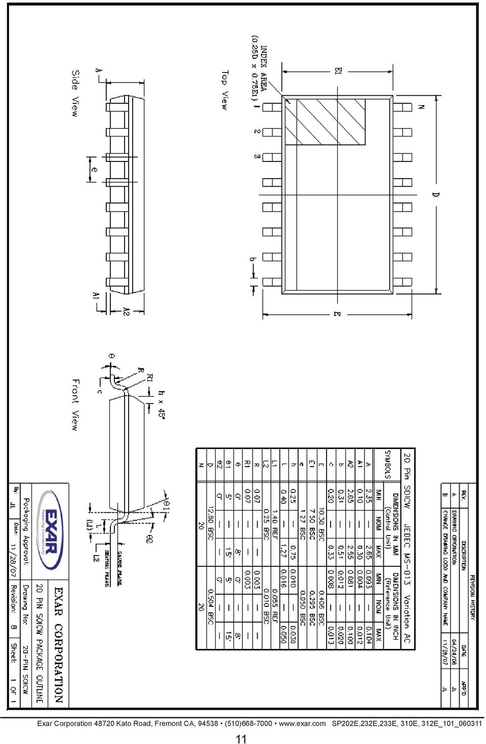
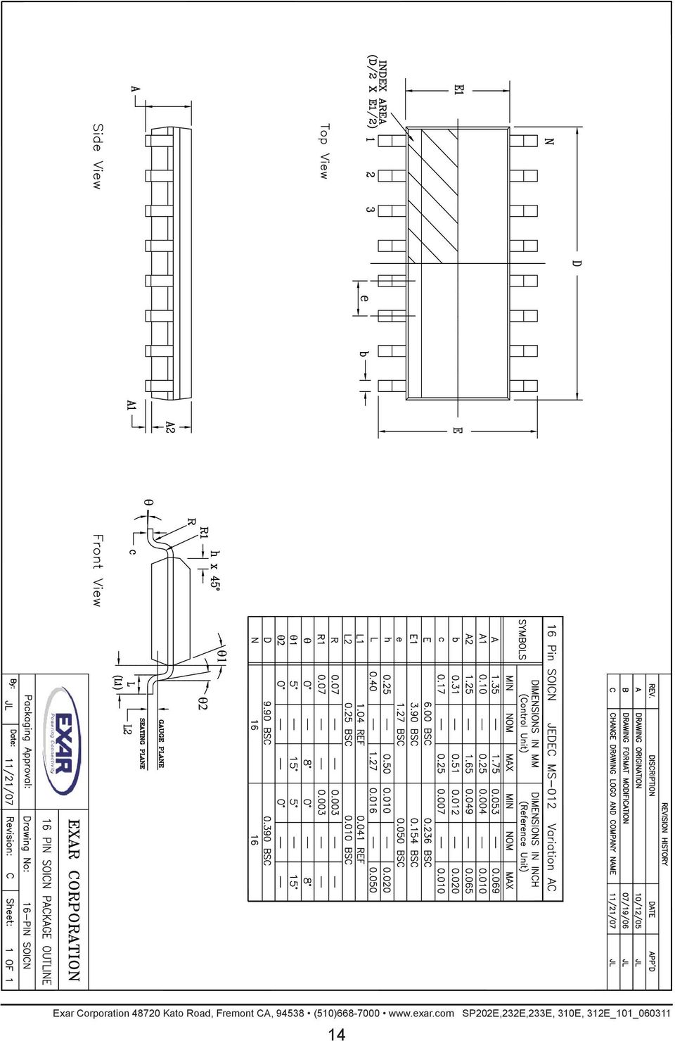
4 PIN ASSIGNMENTS 4

5 DETAILED DESCRIPTION The SP202E, SP232E, SP233E, SP310E and SP312A devices are a family of line driver and receiver pairs that meet the EIA/TIA-232 and V.28 serial communication protocols. The ESD tolerance has been improved on these devices to over +/-15kV for Human Body Model. These devices are pin-to-pin compatible with Exar's 232A, 233A, 310A and 312A as well as popular industry standards. This family of parts offer a 120kbps data rate, 10V/μs slew rate and an onboard charge pump that operates from a single 5V supply using 0.1μF ceramic capacitors. The SP202E, 232E, 233E, 310E and 312E devices have internal charge pump voltage converters which allow them to operate from a single +5V supply. The charge pumps will operate with polarized or non-polarized capacitors ranging from 0.1 to 10µF and will generate the +/-6V needed to generate the RS-232 output levels. The SP233E design offers internal charge pump capacitors. The SP310E provides an ON/OFF input that simultaneously disables the internal charge pump circuit and puts all transmitter and receiver outputs into a high impedance state. The SP312E is identical to the SP310E but with seperate tri-state and shutdown inputs Theory Of Operation The SP202E, SP232E, SP233E, SP310E and SP312E devices are made up of three basic circuit blocks: 1. Drivers, 2. Receivers, and 3. charge pump. Each block is described below. Drivers The drivers are inverting level transmitters that convert TTL or CMOS logic levels to EIA/TIA- 232 levels with an inverted sense relative to the input logic levels. The typical driver output voltage swing is +/-6V. Even under worst case loading conditions of 3k ohms and 2500pF, the driver output is guaranteed to be +/-5.0V minimum, thus satisfying the RS-232 specification. The driver outputs are protected against infinite short-circuits to ground without degradation in reliability. The slew rate of the driver output is internally limited to 30V/μs in order to meet the EIA standards (EIA-232F). Additionally, the driver outputs LOW to HIGH transition meets the montonic output requirements of the standard. 5 DESCRIPTION Receivers The receivers convert EIA/TIA-232 signal levels to inverted TTL or CMOS logic output levels. Since the input is usually from a transmission line, where long cable length and system interference can degrade the signal, the inputs have a typical hysteresis margin of 500mV. This ensures that the receiver is virtually immune to noisy transmission lines. The input thresholds are 0.8V minimum and 2.8V maximum, again well within the +/-3V RS-232 requirements. Should an input be left unconnected, an internal 5kohm pull-down resistor to ground will commit the output of the receiver to a HIGH state. In actual system applications, it is quite possible for signals to be applied to receiver inputs before power is applied to the receiver circuitry. This occurs, for example, when a PC user attempts to print, only to realize that the printer wasn't turned on. In this case an RS-232 signal from the PC will appear on the receiver input at the printer. When the printer power is turned on, the receiver will operate normally. All of these devices are fully protected. Charge pump The charge pump is an Exar patented design and uses a unique approach compared to older less efficiant designs. The charge pump requires 4 external capacitors and uses a four phase voltage shifting technique. The internal power supply consists of a dual charge pump that provides a driver output voltage swing of +/-6V. The internal oscillator controls the four phases of the voltage shifting. A description of each phase follows: Phase 1 Vss charge store and double: The positive terminals of capacitors C1 and C2 are charged from Vcc with their negative terminals initially connected to ground. C1+ is then connected to ground and the stored charge from C1- is superimposed onto C2-. Since C2+ is still connected to Vcc the voltage potential across C2 is now 2 x Vcc. Phase 2 Vss transfer and invert: Phase two connects the negative terminal of C2 to the Vss storage capacitor and the positive terminal of C2 to ground. This transfers the doubled and inverted (V-) voltage onto C4. Meanwhile, capacitor

6 C1 is charged from Vcc to prepare it for its next phase. Phase 3 Vdd charge store and double: Phase three is identical to the first phase. The positive terminals of C1 and C2 are charged from Vcc with their negative terminals initially connected to ground. C1+ is then connected to ground and the stored charge from C1- is superimposed onto C2-. Since C2+ is still connected to Vcc the voltage potential across capacitor C2 is now 2 x Vcc. Phase 4 Vdd transfer: The fourth phase connects the negative terminal of C2 to ground and the positive terminal of C2 to the Vdd storage capacitor. This transfers the doubled (V+) voltage onto C3. Meanwhile, capacitor C1 is charged from Vcc to prepare it for its next phase. The clock rate for the charge pump typically operates at greater than 15kHz allowing the pump to run efficiently with small 0.1uF capacitors. Efficient operation depends on rapid charging and discharging of C1 and C2, therefore capacitors should be mounted as close as possible to the IC and have low ESR (equivalent series resistance). Inexpensive surface mount, ceramic capacitors are ideal for using on charge pump. If polarized capacitors are used the positive and negative terminals should be connected as shown in the typical operating circuit. A diagram of the individual phases are shown in Figure 1. Shutdown (SD) and Enable (EN) features for the SP310E and SP312E Both the SP310E and SP312E have a shutdown / standby mode to conserve power in batterypowered applications. To activate the shutdown mode, which stops the operation of the charge pump, a logic "0" is applied to the appropriate control line. For the SP310E, this control line is the ON/OFF (pin 18) input. Activating the shutdown mode puts the SP310E transmitter and receiver ouptuts into a high impedance condition. For the SP312E, this control line is the SHUTDOWN (pin18) input; this also puts the transmitter outputs in a tri-state mode. The receiver outputs can be tri-stated seperately during normal operation or shutdown by applying a logic "1" on the EN line (pin 1). DESCRIPTION Wake-Up Feature for the SP312E The SP312E has a wake-up feature that keeps the receivers active when the device is placed into shutdown. Table 1 defines the truth table for the Wake-Up function. When only the receivers are activated, the SP312E typically draws less than 5uA supply current. In the case of when a modem is interfaced to a computer in power down mode, the Ring Indicator (RI) signal from the modem would be used to "wake-up" the computer, allowing it to accept data transmission. After the ring indicator has propagated through the SP312E receiver, it can be used to trigger the power management circuitry of the computer to power up the microprocessor, and bring the SD pin of the SP312E to a logic high, taking it out of the shutdown mode. The receiver propagation delay is typically 1us. The enable time for V+ and V- is typically 2ms. After V+ and V- have settled to their final values, a signal can be sent back to the modem on the data terminal ready (DTR) pin signifying that the computer is ready to accept the transmit data. SD EN Power Up/Down Receiver outputs 0 0 Down Enabled 0 1 Down Tri-state 1 0 Up Enabled 1 1 Up Tri-state Table 1. Wake-up Function truth table Pin Strapping for the SP233E To operate properly, the following pairs of pins must be externally wired together as noted in table 2: Pins Wired Together SOICW Two V- pins 10 & 17 Two C2+ pins 12 & 15 Two C- pins 11 & 16 Connect Pins 6 and 9 to GND Table 2. Pin Strapping table for SP233E 6
 voltage onto C3.")
7 + DESCRIPTION V CC - Phase 2 Vss transfer from C2 to C4. Meanwhile C 1 is charged to Vcc + + V CC - Phases 1 and 3: Store/Double. Double charge from C 1 onto C2. C 2 is now charged to -2xVcc + + C C 1 2 e - e - Vss V+ e - C 3 + C C C 1 2 e - e - V+ V- C 3 + C 4 Patented 5,306,954 + V CC - Phase 4 VDD transfer from C2 to C3. Meanwhile C1 is charged to Vcc + + C C 1 2 e - V DD e + e + + V+ V- C 3 + C 4 Figure 1. Charge pump phases ESD TOLERANCE The SP202E, 232E, 233E, 310E and 312E devices incorporates ruggedized ESD cells on all driver outputs and receiver input pins. The ESD structure is improved over our previous family for more rugged applications and environments sensitive to electro-static discharges and associated transients. The improved ESD tolerance is at least +/-15kV Human Body Model without damage nor latch-up. The premise of this ESD test is to simulate the human body's potential to store electrostatic energy and discharge it to an intergrated circuit. The simulation is peformed by using a test model as shown in figure 2. This method will test the IC's capability to withstand an ESD transient during normal handling such as in manufacturing areas where the IC's tend to be handled frequently. R C SW1 R S SW2 The Human Body Model has been the generally accepted ESD testing method for semiconductors. This method is also specified in MIL-STD-883, Method for ESD testing. DC Power Source C S Device Under Test 7 Figure 2. ESD test circuit for Human Body Model

8 TYPICAL PERFORMANCE CHARACTERISTICS Figure 3, SP232E Charge pump waveformsno load (1 = C1+, 2 = C2+, 3 = V+, 4 = V-). Figure 6, Charge pump outputs at start up (1 = Vcc, 2 = V+, 3 = V-). Figure 4, SP232E Charge pump waveforms when fully loaded with 3Kohms (1 = C1+, 2 = C2+, 3 = V+, 4 = V-). Figure 5, Loopback results at 60KHZ and 2500pF load (1 = TXin, 2 = TXout/RXin, 3 = RXout). 8
.")
9 Figure 7, SP202E and SP232E Typical Application circuit Figure 9, SP233ECT Typical Application circuit Figure 8, SP310E Typical Application circuit Figure 10, SP312E Typical Application circuit 9

10 10

11 11
12 12
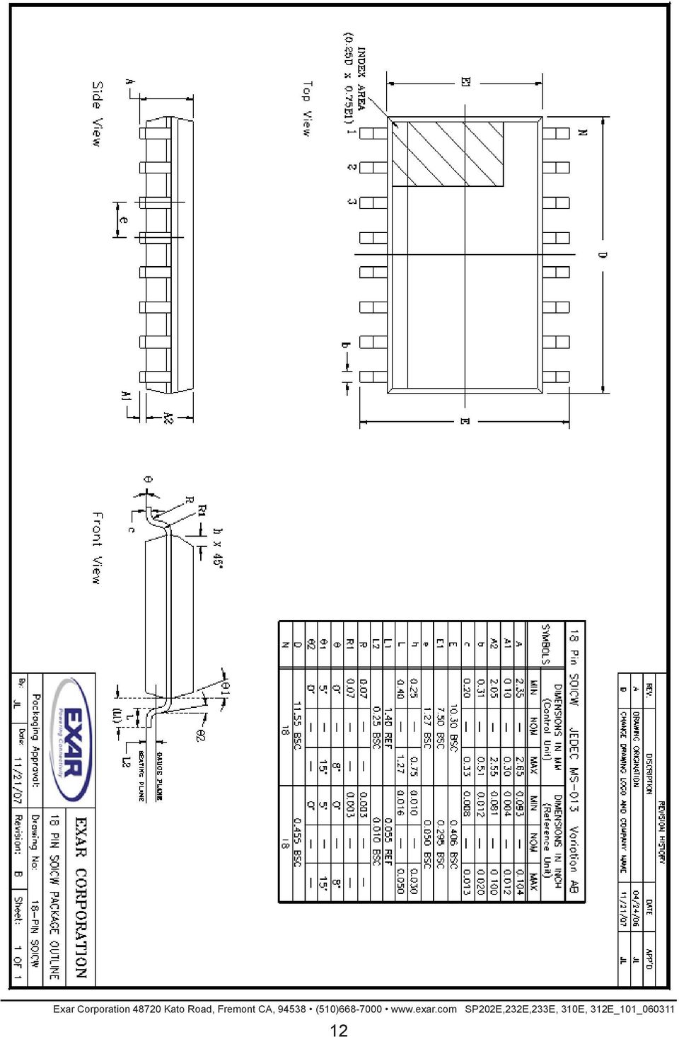
13 13

14 14
15 ORDERING INFORMATION Part number Temperature range Package Type SP202ECN-L 0 0 C to C 16 pin NSOIC SP202ECN-L/TR 0 0 C to C 16 pin NSOIC SP202ECP-L 0 0 C to C 16 pin PDIP SP202ECT-L 0 0 C to C 16 pin SOICW SP202ECT-L/TR 0 0 C to C 16 pin SOICW SP202EEN-L C to C 16 pin NSOIC SP202EEN-L/TR C to C 16 pin NSOIC SP202EEP-L C to C 16 pin PDIP SP202EET-L C to C 16 pin SOICW SP202EET-L/TR C to C 16 pin SOICW SP232ECN-L 0 0 C to C 16 pin NSOIC SP232ECN-L/TR 0 0 C to C 16 pin NSOIC SP232ECP-L 0 0 C to C 16 pin PDIP SP232ECT-L 0 0 C to C 16 pin SOICW SP232ECT-L/TR 0 0 C to C 16 pin SOICW SP232EEN-L C to C 16 pin NSOIC SP232EEN-L/TR C to C 16 pin NSOIC SP232EEP-L C to C 16 pin PDIP SP232EET-L C to C 16 pin SOICW SP232EET-L/TR C to C 16 pin SOICW SP233ECT-L 0 0 C to C 20 pin SOICW SP233ECT-L/TR 0 0 C to C 20 pin SOICW SP233EET-L C to C 20 pin SOICW SP233EET-L/TR C to C 20 pin SOICW SP310ECT-L 0 0 C to C 18 pin SOICW SP310ECT-L/TR 0 0 C to C 18 pin SOICW SP310EET-L C to C 18 pin SOICW SP310EET-L/TR C to C 18 pin SOICW SP312ECT-L 0 0 C to C 18 pin SOICW SP312ECT-L/TR 0 0 C to C 18 pin SOICW SP312EET-L C to C 18 pin SOICW SP312EET-L/TR C to C 18 pin SOICW All packages are available as lead free (RoHS compliant). 15

16 Date Revision Description REVISION HISTORY A Original Sipex Data sheet Generate new Datasheet using Exar format and change revision to Remove IEC Air and Contact ESD ratings. Update ordering information to remove EOL part numbers. Update charge pump description to show regulated charge pump design Remove SP310ECP-L and SP310EEP-L per PDN Notice EXAR Corporation reserves the right to make changes to any products contained in this publication in order to improve design, performance or reliability. EXAR Corporation assumes no representation that the circuits are free of patent infringement. Charts and schedules contained herein are only for illustration purposes and may vary depending upon a user's specific application. While the information in this publication has been carefully checked; no responsibility, however, is assumed for inaccuracies. EXAR Corporation does not recommend the use of any of its products in life support applications where the failure or malfunction of the product can reasonably be expected to cause failure of the life support system or to significantly affect its safety or effectiveness. Products are not authorized for use in such applications unless EXAR Corporation receives, in writting, assurances to its satisfaction that: (a) the risk of injury or damage has been minimized ; (b) the user assumes all such risks; (c) potential liability of EXAR Corporation is adequately protected under the circumstances. Copyright 2011 EXAR Corporation Datasheet June 2011 Send your serial transceiver technical inquiry with technical details to: [email protected] Reproduction, in part or whole, without the prior written consent of EXAR Corporation is prohibited. 16

SP490/491 Full Duplex RS-485 Transceivers
 SP490/491 Full Duplex RS-485 Transceivers FEATURES +5V Only Low Power BiCMOS Driver/Receiver Enable (SP491) RS-485 and RS-422 Drivers/Receivers Pin Compatible with LTC490 and SN75179 (SP490) Pin Compatible
High-Speed, 5 V, 0.1 F CMOS RS-232 Driver/Receivers ADM202/ADM203
 a FEATURES kb Transmission Rate ADM: Small (. F) Charge Pump Capacitors ADM3: No External Capacitors Required Single V Power Supply Meets EIA-3-E and V. Specifications Two Drivers and Two Receivers On-Board
Low Power, 3.3 V, RS-232 Line Drivers/Receivers ADM3202/ADM3222/ADM1385
 Low Power, 3.3 V, RS-232 Line Drivers/Receivers ADM3202/ADM3222/ADM35 FEATURES 460 kbps data rate Specified at 3.3 V Meets EIA-232E specifications 0. μf charge pump capacitors Low power shutdown (ADM3222
+5 V Powered RS-232/RS-422 Transceiver AD7306
 a FEATURES RS- and RS- on One Chip Single + V Supply. F Capacitors Short Circuit Protection Excellent Noise Immunity Low Power BiCMOS Technology High Speed, Low Skew RS- Operation C to + C Operations APPLICATIONS
ICL232. +5V Powered, Dual RS-232 Transmitter/Receiver. Description. Features. Ordering Information. Applications. Functional Diagram.
 ICL August V Powered, Dual RS Transmitter/Receiver Features Meets All RSC and V. Specifications Requires Only Single V Power Supply Onboard Voltage Doubler/Inverter Low Power Consumption Drivers ±V Output
High-Speed, 5 V, 0.1 F CMOS RS-232 Drivers/Receivers ADM222/ADM232A/ADM242
 a FEATURES 200 kb/s Transmission Rate Small (0. F) Charge Pump Capacitors Single V Power Supply Meets All EIA-232-E and V.2 Specifications Two Drivers and Two Receivers On-Board DC-DC Converters V Output
DESCRIPTIO FEATURES APPLICATIO S TYPICAL APPLICATIO. LT1180A/LT1181A Low Power 5V RS232 Dual Driver/Receiver with 0.1µF Capacitors
 FEATRES APPLICATIO S ESD Protection over ±kv ses Small Capacitors: kbaud Operation for R L = k, C L = pf kbaud Operation for R L = k, C L = pf Outputs Withstand ±V Without Damage CMOS Comparable Low Power:
SP3222E/3232E. True +3.0V to +5.5V RS-232 Transceivers. Now Available in Lead Free Packaging
 SP3E/33E True 3.0V to 5.5V RS-3 Transceivers FEATURES Meets true EIA/TIA-3-F Standards from a 3.0V to 5.5V power supply Minimum 10Kbps Data Rate Under Full oad 1µA ow-power Shutdown with Receivers Active
MM74C150 MM82C19 16-Line to 1-Line Multiplexer 3-STATE 16-Line to 1-Line Multiplexer
 MM74C150 MM82C19 16-Line to 1-Line Multiplexer 3-STATE 16-Line to 1-Line Multiplexer General Description The MM74C150 and MM82C19 multiplex 16 digital lines to 1 output. A 4-bit address code determines
CMOS Switched-Capacitor Voltage Converters ADM660/ADM8660
 CMOS Switched-Capacitor Voltage Converters ADM66/ADM866 FEATURES ADM66: Inverts or Doubles Input Supply Voltage ADM866: Inverts Input Supply Voltage ma Output Current Shutdown Function (ADM866) 2.2 F or
AAT4280 Slew Rate Controlled Load Switch
 General Description Features SmartSwitch The AAT4280 SmartSwitch is a P-channel MOSFET power switch designed for high-side load switching applications. The P-channel MOSFET device has a typical R DS(ON)
±15kV ESD-Protected, 1µA, 250kbps, 3.3V/5V, Dual RS-232 Transceivers with Internal Capacitors
 19-1473; Rev 2; 8/4 ±15k ESD-Protected, 1µA, 25kbps, 3.3/5, Dual General Description The are EIA/TIA-232 and.28/.24 communications interfaces with automatic shutdown/ wake-up features, high data-rate capabilities,
MM74C150 MM82C19 16-Line to 1-Line Multiplexer 3-STATE 16-Line to 1-Line Multiplexer
 MM74C150 MM82C19 16-Line to 1-Line Multiplexer 3-STATE 16-Line to 1-Line Multiplexer General Description The MM74C150 and MM82C19 multiplex 16 digital lines to 1 output. A 4-bit address code determines
TOSHIBA Bipolar Linear Integrated Circuit Silicon Monolithic TAR5SB15~TAR5SB50
 TOSHIBA Bipolar Linear Integrated Circuit Silicon Monolithic TARSB~TARSB Point Regulators (Low-Dropout Regulator) TARSB~TARSB The TARSBxx Series is comprised of general-purpose bipolar single-power-supply
POWER-VOLTAGE MONITORING IC WITH WATCHDOG TIMER
 FUJITSU SEMICONDUCTOR DATA SHEET DS04-27402-2E ASSP POWER-VOLTAGE MONITORING IC WITH WATCHDOG TIMER MB3793-42/30 DESCRIPTION The MB3793 is an integrated circuit to monitor power voltage; it incorporates
INTEGRATED CIRCUITS. NE558 Quad timer. Product data Supersedes data of 2001 Aug 03. 2003 Feb 14
 INTEGRATED CIRCUITS Supersedes data of 2001 Aug 03 2003 Feb 14 DESCRIPTION The Quad Timers are monolithic timing devices which can be used to produce four independent timing functions. The output sinks
LM118/LM218/LM318 Operational Amplifiers
 LM118/LM218/LM318 Operational Amplifiers General Description The LM118 series are precision high speed operational amplifiers designed for applications requiring wide bandwidth and high slew rate. They
Silvertel. Ag5200. 1 Features. 2 Description. Power-over-Ethernet Plus Module. IEEE802.3at and IEEE802.3af compliant. Maximum 30W output power
 Silvertel V1.1 November 2012 Datasheet Pb 1 Features IEEE802.3at and IEEE802.3af compliant Maximum 30W output power Dual In-Line (DIL) package size 50.6mm (L) x 30mm (W) Overload, short-circuit and thermal
DSC1001. Low-Power Precision CMOS Oscillator 1.8~3.3V. Features. General Description. Benefits. Block Diagram
 DSC.8~.V LowPower Precision CMOS Oscillator General Description The DSC is a silicon MEMS based CMOS oscillator offering excellent jitter and stability performance over a wide range of supply voltages
MM74HC4538 Dual Retriggerable Monostable Multivibrator
 MM74HC4538 Dual Retriggerable Monostable Multivibrator General Description The MM74HC4538 high speed monostable multivibrator (one shots) is implemented in advanced silicon-gate CMOS technology. They feature
3-input EXCLUSIVE-OR gate. The 74LVC1G386 provides a 3-input EXCLUSIVE-OR function.
 Rev. 02 3 September 2007 Product data sheet 1. General description The provides a 3-input EXCLUSIVE-OR function. The input can be driven from either 3.3 or 5 V devices. This feature allows the use of these
On/Off Controller with Debounce and
 19-4128; Rev ; 5/8 On/Off Controller with Debounce and General Description The is a pushbutton on/off controller with a single switch debouncer and built-in latch. It accepts a noisy input from a mechanical
MM74HC14 Hex Inverting Schmitt Trigger
 MM74HC14 Hex Inverting Schmitt Trigger General Description The MM74HC14 utilizes advanced silicon-gate CMOS technology to achieve the low power dissipation and high noise immunity of standard CMOS, as
Programmable Single-/Dual-/Triple- Tone Gong SAE 800
 Programmable Single-/Dual-/Triple- Tone Gong Preliminary Data SAE 800 Bipolar IC Features Supply voltage range 2.8 V to 18 V Few external components (no electrolytic capacitor) 1 tone, 2 tones, 3 tones
LM1084 5A Low Dropout Positive Regulators
 5A Low Dropout Positive Regulators General Description The LM1084 is a series of low dropout voltage positive regulators with a maximum dropout of 1.5 at 5A of load current. It has the same pin-out as
INTEGRATED CIRCUITS. 74LVC08A Quad 2-input AND gate. Product specification IC24 Data Handbook. 1997 Jun 30
 INTEGRATED CIRCUITS IC24 Data Handbook 1997 Jun 30 FEATURES Wide supply voltage range of 1.2 V to 3.6 V In accordance with JEDEC standard no. 8-1A Inputs accept voltages up to 5.5 V CMOS low power consumption
CA723, CA723C. Voltage Regulators Adjustable from 2V to 37V at Output Currents Up to 150mA without External Pass Transistors. Features.
 CA73, CA73C Data Sheet April 1999 File Number 788. Voltage Regulators Adjustable from V to 37V at Output Currents Up to 1mA without External Pass Transistors The CA73 and CA73C are silicon monolithic integrated
MM74HC273 Octal D-Type Flip-Flops with Clear
 MM74HC273 Octal D-Type Flip-Flops with Clear General Description The MM74HC273 edge triggered flip-flops utilize advanced silicon-gate CMOS technology to implement D-type flipflops. They possess high noise
NTE2053 Integrated Circuit 8 Bit MPU Compatible A/D Converter
 NTE2053 Integrated Circuit 8 Bit MPU Compatible A/D Converter Description: The NTE2053 is a CMOS 8 bit successive approximation Analog to Digital converter in a 20 Lead DIP type package which uses a differential
XR-T5683A PCM Line Interface Chip
 ...the analog plus company TM XR-T5683A PCM Line Interface Chip FEATURES Single 5V Supply Receiver Input Can Be Either Balanced or Unbalanced Up To 8.448Mbps Operation In Both Tx and Rx Directions TTL
MADR-009190-0001TR. Quad Driver for GaAs FET or PIN Diode Switches and Attenuators Rev. 4. Functional Schematic. Features.
 Features High Voltage CMOS Technology Four Channel Positive Voltage Control CMOS device using TTL input levels Low Power Dissipation Low Cost Lead-Free SOIC-16 Plastic Package Halogen-Free Green Mold Compound
MIC4451/4452. General Description. Features. Applications. Functional Diagram V S. 12A-Peak Low-Side MOSFET Driver. Bipolar/CMOS/DMOS Process
 12A-Peak Low-Side MOSFET Driver Bipolar/CMOS/DMOS Process General Description MIC4451 and MIC4452 CMOS MOSFET drivers are robust, efficient, and easy to use. The MIC4451 is an inverting driver, while the
IEC 1000-4-2 ESD Immunity and Transient Current Capability for the SP72X Series Protection Arrays
 IEC 00-4-2 ESD Immunity and Transient Current Capability for the SP72X Series Protection Arrays Application Note July 1999 AN9612.2 Author: Wayne Austin The SP720, SP721, SP723, and SP724 are protection
Photolink- Fiber Optic Receiver PLR135/T1
 Features High PD sensitivity optimized for red light Data : NRZ signal Low power consumption for extended battery life Built-in threshold control for improved noise Margin The product itself will remain
MM74HC174 Hex D-Type Flip-Flops with Clear
 Hex D-Type Flip-Flops with Clear General Description The MM74HC174 edge triggered flip-flops utilize advanced silicon-gate CMOS technology to implement D-type flipflops. They possess high noise immunity,
HIGH SPEED-10 MBit/s LOGIC GATE OPTOCOUPLERS
 DESCRIPTION The, /6 single-channel and /6 dual-channel optocouplers consist of a 5 nm AlGaAS LED, optically coupled to a very high speed integrated photodetector logic gate with a strobable output. This
HT7660. CMOS Switched-Capacitor Voltage Converter. Features. Applications. General Description. Block Diagram
 CMOS Switched-Capacitor Voltage Converter Features Simple conversion of V DD to V DD Cascade connection (two devices are connected, V OUT = 2 V DD ) Boost pin for higher switching frequency Easy to use
MADR-009269-0001TR. Single Driver for GaAs FET or PIN Diode Switches and Attenuators Rev. V1. Functional Schematic. Features.
 Features High Voltage CMOS Technology Complementary Outputs Positive Voltage Control CMOS device using TTL input levels Low Power Dissipation Low Cost Plastic SOIC-8 Package 100% Matte Tin Plating over
Supply voltage Supervisor TL77xx Series. Author: Eilhard Haseloff
 Supply voltage Supervisor TL77xx Series Author: Eilhard Haseloff Literature Number: SLVAE04 March 1997 i IMPORTANT NOTICE Texas Instruments (TI) reserves the right to make changes to its products or to
1 TO 4 CLOCK BUFFER ICS551. Description. Features. Block Diagram DATASHEET
 DATASHEET 1 TO 4 CLOCK BUFFER ICS551 Description The ICS551 is a low cost, high-speed single input to four output clock buffer. Part of IDT s ClockBlocks TM family, this is our lowest cost, small clock
Data Sheet. HFBR-0600Z Series SERCOS Fiber Optic Transmitters and Receivers
 HFBR-0600Z Series SERCOS Fiber Optic Transmitters and Receivers Data Sheet SERCOS SERCOS is a SErial Realtime COmmunication System, a standard digital interface for communication between controls and drives
MADR-009443-0001TR. Quad Driver for GaAs FET or PIN Diode Switches and Attenuators. Functional Schematic. Features. Description. Pin Configuration 2
 Features Functional Schematic High Voltage CMOS Technology Four Channel Positive Voltage Control CMOS device using TTL input levels Low Power Dissipation Low Cost 4x4 mm, 20-lead PQFN Package 100% Matte
Application Note 83 Fundamentals of RS 232 Serial Communications
 Application Note 83 Fundamentals of Serial Communications Due to it s relative simplicity and low hardware overhead (as compared to parallel interfacing), serial communications is used extensively within
Low-power configurable multiple function gate
 Rev. 7 10 September 2014 Product data sheet 1. General description The provides configurable multiple functions. The output state is determined by eight patterns of 3-bit input. The user can choose the
Spread-Spectrum Crystal Multiplier DS1080L. Features
 Rev 1; 3/0 Spread-Spectrum Crystal Multiplier General Description The is a low-jitter, crystal-based clock generator with an integrated phase-locked loop (PLL) to generate spread-spectrum clock outputs
MASW-007070-0001TB. GaAs SPST Switch, Absorptive, Single Supply, DC-4.0 GHz. Features. Pin Configuration 1,2,3,4. Description. Ordering Information
 Features Operates DC - 4 GHz on Single Supply ASIC TTL / CMOS Driver Low DC Power Consumption 50 Ohm Nominal Impedance Test Boards are Available Tape and Reel are Available Lead-Free 4 x 6 mm PQFN Package
TS555. Low-power single CMOS timer. Description. Features. The TS555 is a single CMOS timer with very low consumption:
 Low-power single CMOS timer Description Datasheet - production data The TS555 is a single CMOS timer with very low consumption: Features SO8 (plastic micropackage) Pin connections (top view) (I cc(typ)
ST202 5V POWERED MULTI-CHANNEL RS-232 DRIVERS AND RECEIVERS
 5V POWERED MULTI-CHANNEL RS-232 DRIVERS AND RECEIVERS SUPPLY VOLTAGE RANGE: 4.5 TO 5.5V SUPPLY CURRENT NO LOAD (TYP): 1.5mA TRASMITTER OUTPUT VOLTAGE SWING (TYP): ± 9V TRANSITION SLEW RATE (TYP.): 12V/µs
NCT3941S/S-A Nuvoton 4 Times Linear Fan Driver NCT3941S/S-A
 Nuvoton 4 Times Linear Fan Driver NCT3941S/S-A -I- Revision A4 Table of Content- 1. GENERAL DESCRIPTION...1 2. FEATURES...1 3. APPLICATION...1 4. BLOCK DIAGRAM...2 5. PIN CONFIGURATION AND TYPICAL APPLICATION
ICL7660, ICL7660A. CMOS Voltage Converters. Features. itle L76, L76 A) bjec. ltag. nver s) utho ) eyw s tersi. Applications.
 bjec. ltag. nver s) utho ) eyw s tersi. Applications.") TM ICL, ICLA Data Sheet April 999 File Number. itle L, L A) bjec MO ltag nver s) utho ) eyw s tersi rpor on, arge mp, ltage nvert ltage uble ltage erte X, X, C, CMOS Voltage Converters The Intersil ICL
TM ICL, ICLA Data Sheet April 999 File Number. itle L, L A) bjec MO ltag nver s) utho ) eyw s tersi rpor on, arge mp, ltage nvert ltage uble ltage erte X, X, C, CMOS Voltage Converters The Intersil ICL
29V High Voltage LED Driver
 29V High Voltage LED Driver SP7601 FEATURES Wide Input Voltage Range 4.5V 29V 1.2MHz Constant Frequency Operation Low 0.2V Reference Voltage Adjustable Overcurrent Protection PWM Dimming and Power sequencing
MM54C150 MM74C150 16-Line to 1-Line Multiplexer
 MM54C150 MM74C150 16-Line to 1-Line Multiplexer MM72C19 MM82C19 TRI-STATE 16-Line to 1-Line Multiplexer General Description The MM54C150 MM74C150 and MM72C19 MM82C19 multiplex 16 digital lines to 1 output
DM74LS153 Dual 1-of-4 Line Data Selectors/Multiplexers
 Dual 1-of-4 Line Data Selectors/Multiplexers General Description Each of these data selectors/multiplexers contains inverters and drivers to supply fully complementary, on-chip, binary decoding data selection
4-bit binary full adder with fast carry CIN + (A1 + B1) + 2(A2 + B2) + 4(A3 + B3) + 8(A4 + B4) = = S1 + 2S2 + 4S3 + 8S4 + 16COUT
 + 2(A2 + B2) + 4(A3 + B3) + 8(A4 + B4) = = S1 + 2S2 + 4S3 + 8S4 + 16COUT") Rev. 03 11 November 2004 Product data sheet 1. General description 2. Features The is a high-speed Si-gate CMOS device and is pin compatible with low power Schottky TTL (LSTTL). The is specified in compliance
Rev. 03 11 November 2004 Product data sheet 1. General description 2. Features The is a high-speed Si-gate CMOS device and is pin compatible with low power Schottky TTL (LSTTL). The is specified in compliance
USB to serial chip CH340
 The DataSheet of CH340 (the first) 1 1. Introduction USB to serial chip CH340 English DataSheet Version: 1D http://wch.cn CH340 is a USB bus convert chip and it can realize USB convert to serial interface,
SN28838 PAL-COLOR SUBCARRIER GENERATOR
 Solid-State Reliability Surface-Mount Package NS PACKAE (TOP VIEW) description The SN28838 is a monolithic integrated circuit designed to interface with the SN28837 PALtiming generator in order to generate
PI5C3244 12345678901234567890123456789012123456789012345678901234567890121234567890123456789012345678901212345678901234567890123456789012123456789012
 Features: Near-Zero propagation delay 5-ohm switches connect inputs to outputs when enabled Direct bus connection when switches are ON Ultra Low Quiescent Power (0.2µA Typical) Ideally suited for notebook
400KHz 60V 4A Switching Current Boost / Buck-Boost / Inverting DC/DC Converter
 Features Wide 5V to 32V Input Voltage Range Positive or Negative Output Voltage Programming with a Single Feedback Pin Current Mode Control Provides Excellent Transient Response 1.25V reference adjustable
DATA SHEET. TDA1518BQ 24 W BTL or 2 x 12 watt stereo car radio power amplifier INTEGRATED CIRCUITS
 INTEGRATED CIRCUITS DATA SHEET File under Integrated Circuits, IC01 July 1994 GENERAL DESCRIPTION The is an integrated class-b output amplifier in a 13-lead single-in-line (SIL) plastic power package.
ULC Technology: High-performance gate array package using multiple metal layer CMOS technology featuring sub-micron channel lengths (0.
 SIR Endec for IrDA Applications Integrated Interface Circuits TOIM ULC Technology: High-performance gate array package using multiple metal layer CMOS technology featuring sub-micron channel lengths (0.
AP1509. 150KHz, 2A PWM BUCK DC/DC CONVERTER. Description. Pin Assignments V IN. Applications. Features. (Top View) GND GND. Output AP1509 GND GND
 GND GND. Output AP1509 GND GND") Description Pin Assignments The series are monolithic IC designed for a stepdown DC/DC converter, and own the ability of driving a 2A load without additional transistor. It saves board space. The external
Description Pin Assignments The series are monolithic IC designed for a stepdown DC/DC converter, and own the ability of driving a 2A load without additional transistor. It saves board space. The external
HI-200, HI-201. Features. Dual/Quad SPST, CMOS Analog Switches. Applications. Ordering Information. Functional Diagram FN3121.9
 Data Sheet FN3121.9 Dual/Quad SPST, CMOS Analog Switches HI-200/HI-201 (dual/quad) are monolithic devices comprising independently selectable SPST switches which feature fast switching speeds (HI-200 240ns,
28V, 2A Buck Constant Current Switching Regulator for White LED
 28V, 2A Buck Constant Current Switching Regulator for White LED FP7102 General Description The FP7102 is a PWM control buck converter designed to provide a simple, high efficiency solution for driving
2-Wire/4-Wire Telephone Line Interface. XE0204 Block Diagram
 XE0204 July 2000 2-Wire/4-Wire Telephone Line Interface Description The XE0204 provides a common telephone interface for networks integrating two and four-wire telephone connections. The XE0204 supplies
DATA SHEET. TDA8560Q 2 40 W/2 Ω stereo BTL car radio power amplifier with diagnostic facility INTEGRATED CIRCUITS. 1996 Jan 08
 INTEGRATED CIRCUITS DATA SHEET power amplifier with diagnostic facility Supersedes data of March 1994 File under Integrated Circuits, IC01 1996 Jan 08 FEATURES Requires very few external components High
DM74LS157 DM74LS158 Quad 2-Line to 1-Line Data Selectors/Multiplexers
 September 1986 Revised April 2000 DM74LS157 DM74LS158 Quad 2-Line to 1-Line Data Selectors/Multiplexers General Description These data selectors/multiplexers contain inverters and drivers to supply full
AN460 Using the P82B96 for bus interface
 INTEGRATED CIRCUITS 2001 Feb 14 IC12a and IC28 Data Handbook The P82B96 offers many different ways in which it can be used as a bus interface. In its simplest application it can be used as an interface
DM74LS191 Synchronous 4-Bit Up/Down Counter with Mode Control
 August 1986 Revised February 1999 DM74LS191 Synchronous 4-Bit Up/Down Counter with Mode Control General Description The DM74LS191 circuit is a synchronous, reversible, up/ down counter. Synchronous operation
S112-XHS. Description. Features. Agency Approvals. Applications. Absolute Maximum Ratings. Schematic Diagram. Ordering Information
 Description Features The S112-X is a bi-directional, single-pole, single-throw, normally open multipurpose solid-state relay. The circuit is composed of one input IR LED with a series limiting resistor
HT9170 DTMF Receiver. Features. General Description. Selection Table
 DTMF Receiver Features Operating voltage: 2.5V~5.5V Minimal external components No external filter is required Low standby current (on power down mode) General Description The HT9170 series are Dual Tone
DM74121 One-Shot with Clear and Complementary Outputs
 June 1989 Revised July 2001 DM74121 One-Shot with Clear and Complementary Outputs General Description The DM74121 is a monostable multivibrator featuring both positive and negative edge triggering with
CD4013BC Dual D-Type Flip-Flop
 CD4013BC Dual D-Type Flip-Flop General Description The CD4013B dual D-type flip-flop is a monolithic complementary MOS (CMOS) integrated circuit constructed with N- and P-channel enhancement mode transistors.
MAX220/MAX232/MAX232A
 -Powered, Multichannel General Description The MAX0 MAX family of line drivers/receivers is intended for all EIA/TIA-E and V./V. communications interfaces, particularly applications where ±V is not available.
INTEGRATED CIRCUITS. 74F153 Dual 4-line to 1-line multiplexer. Product specification 1996 Jan 05 IC15 Data Handbook
 INTEGRATED CIRCUITS 1996 Jan 05 IC15 Data Handbook FEATURES Non-inverting outputs Separate enable for each section Common select inputs See 74F253 for 3-State version PIN CONFIGURATION Ea 1 S1 2 I3a 3
VT-802 Temperature Compensated Crystal Oscillator
 T-802 Temperature Compensated Crystal Oscillator T-802 Description ectron s T-802 Temperature Compensated Crystal Oscillator (TCXO) is a quartz stabilized, CMOS output, analog temperature compensated oscillator,
MM74HCT373 MM74HCT374 3-STATE Octal D-Type Latch 3-STATE Octal D-Type Flip-Flop
 3-STATE Octal D-Type Latch 3-STATE Octal D-Type Flip-Flop General Description The MM74HCT373 octal D-type latches and MM74HCT374 Octal D-type flip flops advanced silicongate CMOS technology, which provides
RS-422 and RS-485 Application Note
 RS-422 and RS-485 Application Note International Headquarters B&B Electronics Mfg. Co. Inc. 707 Dayton Road -- P.O. Box 1040 -- Ottawa, IL 61350 USA Phone (815) 433-5100 -- General Fax (815) 433-5105 Home
AUIPS71411G CURRENT SENSE HIGH SIDE SWITCH
 February, 21st 2010 Automotive grade AUIPS71411G CURRENT SENSE HIGH SIDE SWITCH Features Suitable 24V battery operation Over current shutdown Over temperature shutdown Current sensing Active clamp Low
How To Connect A 10Gbps Sfp+ Bi-Directional Transceiver To A Single Mode Fiber With A Single Power Cell (Sfp+) To A Power Cell With A Power Source (Sf) (Sfl) (
 To A Power Cell With A Power Source (Sf) (Sfl) (") Features 10Gbps SFP+ Bi-Directional Transceiver, 20km Reach 1270/1330nm TX / 1330/1270 nm RX Supports 9.95Gb/s to 10.3Gb/s data rates Simplex LC Connector Bi-Directional SFP+ Optical Transceiver Single
Features 10Gbps SFP+ Bi-Directional Transceiver, 20km Reach 1270/1330nm TX / 1330/1270 nm RX Supports 9.95Gb/s to 10.3Gb/s data rates Simplex LC Connector Bi-Directional SFP+ Optical Transceiver Single
FEATURES DESCRIPTION APPLICATIONS BLOCK DIAGRAM. PT2248 Infrared Remote Control Transmitter
 Infrared Remote Control Transmitter DESCRIPTION PT2248 is an infrared remote control transmitter utilizing CMOS Technology. It is capable of 18 functions and a total of 75 commands. Single-shot and continuous
High-Speed, Low-Power, 3V/5V, Rail-to-Rail, Single-Supply Comparators MAX941/MAX942/ MAX944. General Description. Features. Ordering Information
 General Description The MAX941/MAX94/ are single/dual/quad highspeed comparators optimized for systems powered from a 3V or 5V supply. These devices combine high speed, low power, and rail-to-rail inputs.
ICS379. Quad PLL with VCXO Quick Turn Clock. Description. Features. Block Diagram
 Quad PLL with VCXO Quick Turn Clock Description The ICS379 QTClock TM generates up to 9 high quality, high frequency clock outputs including a reference from a low frequency pullable crystal. It is designed
Order code Temperature range Package Packaging
 ST485B ST485C Low power RS-485/RS-422 transceiver Features Low quiescent current: 300 µa Designed for RS-485 interface application - 7 V to 12 V common mode input voltage range Driver maintains high impedance
DS1621 Digital Thermometer and Thermostat
 Digital Thermometer and Thermostat www.dalsemi.com FEATURES Temperature measurements require no external components Measures temperatures from 55 C to +125 C in 0.5 C increments. Fahrenheit equivalent
CD40174BC CD40175BC Hex D-Type Flip-Flop Quad D-Type Flip-Flop
 Hex D-Type Flip-Flop Quad D-Type Flip-Flop General Description The CD40174BC consists of six positive-edge triggered D- type flip-flops; the true outputs from each flip-flop are externally available. The
DG2302. High-Speed, Low r ON, SPST Analog Switch. Vishay Siliconix. (1-Bit Bus Switch with Level-Shifter) RoHS* COMPLIANT DESCRIPTION FEATURES
 RoHS* COMPLIANT DESCRIPTION FEATURES") High-Speed, Low r ON, SPST Analog Switch (1-Bit Bus Switch with Level-Shifter) DG2302 DESCRIPTION The DG2302 is a high-speed, 1-bit, low power, TTLcompatible bus switch. Using sub-micron CMOS technology,
High-Speed, Low r ON, SPST Analog Switch (1-Bit Bus Switch with Level-Shifter) DG2302 DESCRIPTION The DG2302 is a high-speed, 1-bit, low power, TTLcompatible bus switch. Using sub-micron CMOS technology,
AP1506. 150KHz, 3A PWM BUCK DC/DC CONVERTER. Pin Assignments. Description. Features. Applications. ( Top View ) 5 SD 4 FB 3 Gnd 2 Output 1 V IN
 5 SD 4 FB 3 Gnd 2 Output 1 V IN") Description Pin Assignments The series are monolithic IC designed for a stepdown DC/DC converter, and own the ability of driving a 3A load without external transistor. Due to reducing the number of external
Description Pin Assignments The series are monolithic IC designed for a stepdown DC/DC converter, and own the ability of driving a 3A load without external transistor. Due to reducing the number of external
ADM206E/ADM207E/ADM208E/ADM211E/ADM213E
 EMI/EMC-Compliant, ± kv ESD Protected, RS- Line Drivers/Receivers ADM6E/ADM7E/ADM8E/ADME/ADME FEATURES Complies with 89/6/EEC EMC directive ESD protection to IEC 000-4- (80-) Contact discharge: ±8 kv Air-gap
LM2704 Micropower Step-up DC/DC Converter with 550mA Peak Current Limit
 Micropower Step-up DC/DC Converter with 550mA Peak Current Limit General Description The LM2704 is a micropower step-up DC/DC in a small 5-lead SOT-23 package. A current limited, fixed off-time control
SELECTION GUIDE. Nominal Input
 www.murata-ps.com NKE Series FEATURES RoHS Compliant Sub-Miniature SIP & DIP Styles 3kVDC Isolation UL Recognised Wide Temperature performance at full 1 Watt load, 40 C to 85 C Increased Power Density
Cool-Power PI33xx-x0. 8 V to 36 V IN Cool-Power ZVS Buck Regulator Family. Product Description. Features & Benefits. Applications. Package Information
 Cool-Power PI33xx-x0 8 V to 36 V IN Cool-Power ZVS Buck Regulator Family Product Description The PI33xx-x0 is a family of high efficiency, wide input range DC-DC ZVS-Buck regulators integrating controller,
Features. Symbol JEDEC TO-220AB
 Data Sheet June 1999 File Number 2253.2 3A, 5V,.4 Ohm, N-Channel Power MOSFET This is an N-Channel enhancement mode silicon gate power field effect transistor designed for applications such as switching
Product Datasheet P1110 915 MHz RF Powerharvester Receiver
 DESCRIPTION The Powercast P1110 Powerharvester receiver is an RF energy harvesting device that converts RF to DC. Housed in a compact SMD package, the P1110 receiver provides RF energy harvesting and power
AP331A XX G - 7. Lead Free G : Green. Packaging (Note 2)
") Features General Description Wide supply Voltage range: 2.0V to 36V Single or dual supplies: ±1.0V to ±18V Very low supply current drain (0.4mA) independent of supply voltage Low input biasing current:
Features General Description Wide supply Voltage range: 2.0V to 36V Single or dual supplies: ±1.0V to ±18V Very low supply current drain (0.4mA) independent of supply voltage Low input biasing current:
. HIGH SPEED .LOW POWER DISSIPATION .COMPATIBLE WITH TTL OUTPUTS M54HCT27 M74HCT27 TRIPLE 3-INPUT NOR GATE. tpd = 9 ns (TYP.
 M54HCT27 M74HCT27 TRIPLE 3-INPUT NOR GATE. HIGH SPEED tpd = 9 ns (TYP.) AT VCC =5V.LOW POWER DISSIPATION I CC =1µA (MAX.) AT T A =25 C.COMPATIBLE WITH TTL OUTPUTS VIH = 2V (MIN.) VIL = 0.8V (MAX) OUTPUT
The 74LVC1G11 provides a single 3-input AND gate.
 Rev. 8 17 September 2015 Product data sheet 1. General description The provides a single 3-input AND gate. The input can be driven from either 3.3 V or 5 V devices. This feature allows the use of this
High Common-Mode Rejection. Differential Line Receiver SSM2141. Fax: 781/461-3113 FUNCTIONAL BLOCK DIAGRAM FEATURES. High Common-Mode Rejection
 a FEATURES High Common-Mode Rejection DC: 00 db typ 60 Hz: 00 db typ 20 khz: 70 db typ 40 khz: 62 db typ Low Distortion: 0.00% typ Fast Slew Rate: 9.5 V/ s typ Wide Bandwidth: 3 MHz typ Low Cost Complements
ICS650-44 SPREAD SPECTRUM CLOCK SYNTHESIZER. Description. Features. Block Diagram DATASHEET
 DATASHEET ICS650-44 Description The ICS650-44 is a spread spectrum clock synthesizer intended for video projector and digital TV applications. It generates three copies of an EMI optimized 50 MHz clock