Flex Circuits for the ATLAS Pixel Detector
|
|
|
- Barnard Park
- 9 years ago
- Views:
Transcription
1 Flex Circuits for the ATLAS Pixel Detector P. Skubic University of Oklahoma

2 Outline ATLAS pixel detector ATLAS prototype Flex hybrid designs Performance simulations Performance measurements Wire bonding experience (CLEO III) Vendors Test beam results Conclusions
 Vendors Test beam")
3 The ATLAS Pixel Detector

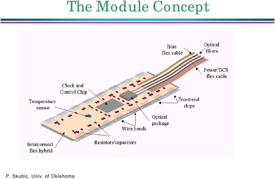
4 The Module Concept
5 Assumptions for the Design of the Flex Hybrid All specifications for the Front End chip and the MCC pinout, pin description, and geographical location are from Darbo, et al.; ATLAS Module Demonstrator - Pixel Module Specifications. ( Revision 2.0) Current specification of the chips.» FE Chip:» MCC: 40 ma for 3.0 V analog power 50 ma for 1.5 V analog power 50 ma for 3.0 V digital power 200 ma for 3.0 V digital Power 150 mv voltage drop in the power lines over the length of the module Each power line can be one bus feeding different pads on the FE and MCC chips.

6 Block Diagram of Signal Connections

7 Module Assembly at OU All modules assembled with conductive epoxy to attach SMD s 4 FE only flex hybrid dummy module Kapton tape or cover layer FE s FH Kapton tape or cover layer Si

8 4 FE Only Module (OU)

9 Complete Flex Hybrid Module (OU)

10 Prototype 1.1 Design Term. U bus Term. Driver H bus Driver Term. If simulations agree with measurements H bus layout

11 Flex Hybrid V1.1

12 Simulations with Maxwell-Spice Link

13 Simulation of Dual Trace Model with Adjacent GND

14 Simulation of Dual Trace Model with Adjacent GND

15 Simulation of Dual Trace Model With Adjacent GND

16 Simulation of Dual Trace Model With Adjacent GND

17 Flex Hybrid signal measurements Typical CCK - DGND signal Typical LV1p - LV1n signal 328 mv/div mv/div. 2 ns/div. 50 ns/div. Typical CCK - DGND signal Typical LV1p - LV1n signal mv/div mv/div. 20 ns/div. 2 ns/div.

18 Thresholds for a typical FE chip on Flex module

19 Noise for a typical FE chip on Flex module

20 Vendor experience GE (General Electric Corporate Research and Development), NY Completed delivery of CLEOIII flex circuits Nov. 98 Final cost (11 & 12 flex/frame) $175/flex Design rules used on CLEO III flex connector 60 µm spaces and 40 µm traces Via cover pad = 75 µm square; 25 µm plated hole 75 µm wide bond pads on 100 µm pitch; two interleaved rows Double sided 512 vias

21 CLEO III Flex Connector
22 CLEOIII Wire Bonding Experience µm pitch wire bonds x 244 flex circuits ~ 250K wire bonds Automated wire bonder tuning» 47 bonds» Average pull strength 7.3, gm std. dev. 0.9 gm» Min. 5.7 gm» Operating parameters (power, time, force, etc.) optimized for consistent results on two different bonding stations of same model» Support of piece being wire bonded must be consistent
23 CLEOIII Si3 Wire Bonding Experience (cont.) Power Number Mean Std Dev Std Err Mean Power Setting
24 CLEOIII Si3 Wire Bonding Experience (cont.) Wire bond quality can be discerned by visual inspection Foot 1.5x wire diam.. Round No tail Oval Tail Both bond and pad are in focus Top of bond is above pad Example of smashed bond on production (hybridless) starter NL2-03. Example of a good wirebond on flex bond pads.
25 CLEOIII Wire Bonding Experience (cont.) Conclusion: Uniform high pull strength bonds are made:» Using parameters that form a tail on the bonds» By adjusting power and/or bond-time as needed to yield bond foot deformation ~1.5x wire diameter 81K wire bonds to date - 3 failures (due to pad delamination) Wire bonds are encapsulated with Dow Corning Sylgard 186 Note: R&D Circuits claims that 15 gm wire bonds are obtained by controlling Au purity
26 Vendors CERN: produced over 50 flex circuits» Design rules: 75 µm traces and spaces» Metal: 16 µm Cu, 2 µm Ni, 0.1 µm Au» Via s: 130 µm cover pads, 70 µm holes» Substrate: 50 µm thick Kapton» Cover layers: 60 µm thick cover (Pyralux) on top and bottom» Over 600 via s
27 Vendors (con t) Compunetics, Inc. (Monroeville, PA): produced 42 flex circuits» Design rules: 75 µm traces and spaces» Metal: 16 µm Cu, 2 µm Ni, 0.1 µm Au on solder pads and 1.5 µm on bond pads» Via s: 130 µm cover pads, 50 µm holes» Substrate: 25 µm thick Upilex» Cover layers: 13 µm thick (Intek) on top and bottom» Over 600 via s
28 Vendors (con t) R&D Circuits (Edison, N.J.): produced several non-functional samples» Design rules: 75 µm traces and spaces» Metal: 16 µm Cu, 2 µm Ni, 0.1 µm Au on solder pads and 1.5 µm on bond pads» Via s: 130 µm cover pads, 50 µm holes» Substrate: 25 µm thick Kapton» Cover layers: none on samples» Over 600 via s
29 Vendors (cont.) Assembly: AMA; Sunnyvale, CA» mounted SMD s on 10 flex circuits Testing: Microcontact; Switzerland» Tested flex circuits produced by CERN before Ni and Au plating Test verification: SUNY- Albany» Developing procedures for testing flex hybrids before and after SMD mounting
30 Flex Hybrid Module (LBL) in CERN test beam (May 99) SnPb bumps 200 µm thick detector 16 FE chips MCC readout
31 Module in test beam: Efficiency vs Time
32 Module in test beam: Resolution
33 Module resolution from test beam measurements One pixel cluster:» flat top x 2 = 43.4 µm» σ = 6.0 µm Two pixel clusters: σ = 6.5 µm One and two pixel clusters: σ = 13.8 µm
34 Charge Sharing from test beam measurements
35 Conclusions Flex circuits have been made which provide required pixel module interconnections» Material constraints favor aggressive non-standard design rules Measurements indicate that the designs meet signal integrity requirements Wire bonding to flex is not trivial, but can be understood» Quality of bond can be evaluated by visual inspection No problems attributable to Flex Hybrid or layout have been observed to date
Ball Grid Array (BGA) Technology
 Technology") Chapter E: BGA Ball Grid Array (BGA) Technology The information presented in this chapter has been collected from a number of sources describing BGA activities, both nationally at IVF and reported elsewhere
Chapter E: BGA Ball Grid Array (BGA) Technology The information presented in this chapter has been collected from a number of sources describing BGA activities, both nationally at IVF and reported elsewhere
Mounting Instructions for SP4 Power Modules
 Mounting Instructions for SP4 Power Modules Pierre-Laurent Doumergue R&D Engineer Microsemi Power Module Products 26 rue de Campilleau 33 520 Bruges, France Introduction: This application note gives the
Designing with High-Density BGA Packages for Altera Devices
 2014.12.15 Designing with High-Density BGA Packages for Altera Devices AN-114 Subscribe As programmable logic devices (PLDs) increase in density and I/O pins, the demand for small packages and diverse
Silicon Lab Bonn. Physikalisches Institut Universität Bonn. DEPFET Test System Test Beam @ DESY
 Silicon Lab Bonn Physikalisches Institut Universität Bonn DEPFET Test System Test Beam @ DESY H. Krüger, EUDET Brainstorming, 3/4.11.2005 1 SI LAB DEPFET Prototype System DEPFET sensors 64 x 128 pixels,
1.Introduction. Introduction. Most of slides come from Semiconductor Manufacturing Technology by Michael Quirk and Julian Serda.
 .Introduction If the automobile had followed the same development cycle as the computer, a Rolls- Royce would today cost $00, get one million miles to the gallon and explode once a year Most of slides
NBB-402. RoHS Compliant & Pb-Free Product. Typical Applications
 Typical Applications Narrow and Broadband Commercial and Military Radio Designs Linear and Saturated Amplifiers 0 RoHS Compliant & Pb-Free Product NBB-402 CASCADABLE BROADBAND GaAs MMIC AMPLIFIER DC TO
Winbond W2E512/W27E257 EEPROM
 Construction Analysis Winbond W2E512/W27E257 EEPROM Report Number: SCA 9703-533 Global Semiconductor Industry the Serving Since 1964 15022 N. 75th Street Scottsdale, AZ 85260-2476 Phone: 602-998-9780 Fax:
Development of a Design & Manufacturing Environment for Reliable and Cost-Effective PCB Embedding Technology
 Development of a Design & Manufacturing Environment for Reliable and Cost-Effective PCB Embedding Technology Outline Introduction CAD design tools for embedded components Thermo mechanical design rules
CIRCUITS AND SYSTEMS- Assembly and Printed Circuit Board (PCB) Package Mohammad S. Sharawi ASSEMBLY AND PRINTED CIRCUIT BOARD (PCB) PACKAGE
 Package Mohammad S. Sharawi ASSEMBLY AND PRINTED CIRCUIT BOARD (PCB) PACKAGE") ASSEMBLY AND PRINTED CIRCUIT BOARD (PCB) PACKAGE Mohammad S. Sharawi Electrical Engineering Department, King Fahd University of Petroleum and Minerals Dhahran, 31261 Saudi Arabia Keywords: Printed Circuit
ASSEMBLY AND PRINTED CIRCUIT BOARD (PCB) PACKAGE Mohammad S. Sharawi Electrical Engineering Department, King Fahd University of Petroleum and Minerals Dhahran, 31261 Saudi Arabia Keywords: Printed Circuit
Compliant Terminal Technology Summary Test Report
 Engineering Report ER04100 October 5th, 2004 Revision A Copyright Autosplice Inc., September 2004 Table of Contents Summary Overview 3 Compliant Terminal Specifications 3 Test Plan 4 Test Conditions 4
HDI. HDI = High Density Interconnect. Kenneth Jonsson Bo Andersson. NCAB Group
 HDI HDI = High Density Interconnect Kenneth Jonsson Bo Andersson NCAB Group Definitions / Standards (IPC) Pros & Cons Key equipment Build-ups Choice of material Design rules IPC HDI reliability (µvia stacked
PRINTED CIRCUIT BOARD SURFACE FINISHES - ADVANTAGES AND DISADVANTAGES
 PRINTED CIRCUIT BOARD SURFACE FINISHES - ADVANTAGES AND DISADVANTAGES By Al Wright, PCB Field Applications Engineer Epec Engineered Technologies Anyone involved within the printed circuit board (PCB) industry
Flexible Circuit Simple Design Guide
 Flexible Circuit Simple Design Guide INDEX Flexible Circuit Board Types and Definitions Design Guides and Rules Process Flow Raw Material Single Side Flexible PCB Single Side Flexible PCB (Cover layer
Specification for Electroless Nickel/ Electroless Palladium/ Immersion Gold (ENEPIG) Plating for Printed Circuit Boards
 Plating for Printed Circuit Boards") Specification for Electroless Nickel/ Electroless Palladium/ Immersion Gold (ENEPIG) Plating for Printed Circuit Boards Developed by the Plating Processes Subcommittee (4-14) of the Fabrication Processes
Specification for Electroless Nickel/ Electroless Palladium/ Immersion Gold (ENEPIG) Plating for Printed Circuit Boards Developed by the Plating Processes Subcommittee (4-14) of the Fabrication Processes
Figure 1 (end) Application Specification 114 13088 provides application requirements for MICTOR Right Angle Connectors for SMT PC Board Applications
 Application Specification 114 13088 provides application requirements for MICTOR Right Angle Connectors for SMT PC Board Applications") This specification covers requirements for application of MICTOR Vertical Board to Board Plugs and Receptacles designed for pc boards. The connectors have an in row contact spacing on 0.64 [.025] centerlines.
This specification covers requirements for application of MICTOR Vertical Board to Board Plugs and Receptacles designed for pc boards. The connectors have an in row contact spacing on 0.64 [.025] centerlines.
A Manufacturing Technology Perspective of: Embedded Die in Substrate and Panel Based Fan-Out Packages
 A Manufacturing Technology Perspective of: Embedded Die in Substrate and Panel Based Fan-Out Packages Bernd K Appelt Director WW Business Development April 24, 2012 Table of Content Definitions Wafer Level
Advanced Technologies and Equipment for 3D-Packaging
 Advanced Technologies and Equipment for 3D-Packaging Thomas Oppert Semicon Russia 15 th May 2014 Outline Short Company Introduction Electroless Plating on Wafer Level Ultra-SB 2 - Wafer Level Solder Balling
Prototyping Printed Circuit Boards
 Prototyping Printed Circuit Boards From concept to prototype to production. (HBRC) PCB Design and Fabrication Agenda Introduction Why PCBs? Stage 1 Understanding the rules Stage 2 Planning the board. Stage
San Francisco Circuits, Inc.
 Your Doorway to Innovation San Francisco Circuits, Inc. Bridging Concepts with Reality Flex PCB Introduction to Flex Circuits What is Flex Circuits? From Wikipedia - a technology for assembling electronic
Copyright 2008 IEEE. Reprinted from ECTC2008 Proceedings.
 Copyright 2008 IEEE. Reprinted from ECTC2008 Proceedings. This material is posted here with permission of the IEEE. Such permission of the IEEE does not in any way imply IEEE endorsement of any of Amkor
Miniaturizing Flexible Circuits for use in Medical Electronics. Nate Kreutter 3M
 Miniaturizing Flexible Circuits for use in Medical Electronics Nate Kreutter 3M Drivers for Medical Miniaturization Market Drivers for Increased use of Medical Electronics Aging Population Early Detection
POWER FORUM, BOLOGNA 20-09-2012
 POWER FORUM, BOLOGNA 20-09-2012 Convertitori DC/DC ad alta densità di potenza e bassa impedenza termica. Massimo GAVIOLI. Senior Field Application Engineer. Intersil SIMPLY SMARTER Challenges when Designing
THE CMS PIXEL DETECTOR: FROM PRODUCTION TO COMMISSIONING
 THE CMS PIXEL DETECTOR: FROM PRODUCTION TO COMMISSIONING VINCENZO CHIOCHIA On behalf of the CMS Collaboration University of Zürich, Physik-Institut, Winterthurerstr. 190 Zürich, CH-8057, Switzerland The
PRODUCT SPECIFICATION
 ipass TM / ipass+ TM 0.8 mm PITCH I/O CONNECTOR SYSTEM EXTERNAL ipass / ipass+ of TABLE OF CONTENTS.0 SCOPE... 3.0 PRODUCT DESCRIPTION... 3. PRODUCT NAME AND SERIES NUMBER(S)... 3. DIMENSION, MATERIALS,
 Preface xiii Introduction xv 1 Planning for surface mount design General electronic products 3 Dedicated service electronic products 3 High-reliability electronic products 4 Defining the environmental
Flex Circuit Design and Manufacture.
 Flex Circuit Design and Manufacture. Hawarden Industrial Park, Manor Lane, Deeside, Flintshire, CH5 3QZ Tel 01244 520510 Fax 01244 520721 [email protected] www.merlincircuit.co.uk Flex Circuit
The quadrature signals and the index pulse are accessed through five 0.025 inch square pins located on 0.1 inch centers.
 Quick Assembly Two and Three Channel Optical Encoders Technical Data HEDM-550x/560x HEDS-550x/554x HEDS-560x/564x Features Two Channel Quadrature Output with Optional Index Pulse Quick and Easy Assembly
Silicon Seminar. Optolinks and Off Detector Electronics in ATLAS Pixel Detector
 Silicon Seminar Optolinks and Off Detector Electronics in ATLAS Pixel Detector Overview Requirements The architecture of the optical links for the ATLAS pixel detector ROD BOC Optoboard Requirements of
Specializing in Open Cavity Packages & Complete IC Assembly Services ISO 9001:2008 Certified and ITAR Registered
 TowerJazz Global Symposium Specializing in Open Cavity Packages & Complete IC Assembly Services and TowerJazz Global Symposium Quik-Pak a division of Delphon Industries 2011 Gold Sponsor and TowerJazz
Product Datasheet P1110 915 MHz RF Powerharvester Receiver
 DESCRIPTION The Powercast P1110 Powerharvester receiver is an RF energy harvesting device that converts RF to DC. Housed in a compact SMD package, the P1110 receiver provides RF energy harvesting and power
Chip-on-board Technology
 Hybrid Technology The trend in electronics is to continue to integrate more and more functions and numbers of components into a single, smaller assembly. Hybrid circuit technology is a key method of increasing
Electronic Board Assembly
 Electronic Board Assembly ERNI Systems Technology Systems Solutions - a one stop shop - www.erni.com Contents ERNI Systems Technology Soldering Technologies SMT soldering THR soldering THT soldering -
Automated Contact Resistance Tester CR-2601
 Automated Contact Resistance Tester CR-2601 What s New What s New Summary of Hardware Improvements: The middle Stiffener has been improved and no longer comes in direct contact with the main board thus
Five Year Projections of the Global Flexible Circuit Market
 Five Year Projections of the Global Flexible Circuit Market Robert Turunen and Dominique Numakura, DKN Research And James J. Hickman, PhD, Hickman Associates Inc Summary A new market research process has
DESIGN GUIDELINES FOR LTCC
 DESIGN GUIDELINES FOR LTCC HERALOCK HL2000 MATERIALS SYSTEM Preliminary Guideline Release 1.0 CONTENTS 1. INTRODUCTION 1.1. GLOSSARY OF TERMS 1.2. LTCC PROCESS FLOW DIAGRAM 1.3. UNITS OF MEASURE 2. PROCESSING
What is surface mount?
 A way of attaching electronic components to a printed circuit board The solder joint forms the mechanical and electrical connection What is surface mount? Bonding of the solder joint is to the surface
Multilevel Socket Technologies
 Multilevel Socket Technologies High Performance IC Sockets And Test Adapters Overview Company Overview Over 5,000 products High Performance Adapters and Sockets Many Custom Designs & Turn-Key Solutions
NBB-300 Cascadable Broadband GaAs MMIC Amplifier DC to 12GHz
 Cascadable Broadband GaAs MMIC Amplifier DC to 12GHz NBB-300 The NBB-300 cascadable broadband InGaP/GaAs MMIC amplifier is a low-cost, high-performance solution for general purpose RF and microwave amplification
Good Boards = Results
 Section 2: Printed Circuit Board Fabrication & Solderability Good Boards = Results Board fabrication is one aspect of the electronics production industry that SMT assembly engineers often know little about.
INFN Rome Silicon Microstrip Detector for SBS F. De Persio S. Kiprich - F. Meddi G.M. Urciuoli
 INFN Rome Silicon Microstrip Detector for SBS F. De Persio S. Kiprich - F. Meddi G.M. Urciuoli 1 Summary 1) About us: Presentation of the JLAB12 INFN Roma group. 2) Silicon Detector Advantages on SBS:
23-26GHz Reflective SP4T Switch. GaAs Monolithic Microwave IC in SMD leadless package
 CHS2411-QDG Description GaAs Monolithic Microwave IC in SMD leadless package The CHS2411-QDG (CHS2412-QDG, see Note) is a monolithic reflective SP4T switch in K-Band. Positive supply voltage only is required.
Dual Integration - Verschmelzung von Wafer und Panel Level Technologien
 ERÖFFNUNG DES INNOVATIONSZENTRUMS ADAPTSYS Dual Integration - Verschmelzung von Wafer und Panel Level Technologien Dr. Michael Töpper BDT Introduction Introduction Why do we need such large machines to
Status of the design of the TDC for the GTK TDCpix ASIC
 Status of the design of the TDC for the GTK TDCpix ASIC Gianluca Aglieri Rinella, Lukas Perktold DLL design review meeting, 16 03 2011 Outline Introduction Purpose and objectives Reminder Challenges of
CMS Tracker module / hybrid tests and DAQ development for the HL-LHC
 CMS Tracker module / hybrid tests and DAQ development for the HL-LHC S. Mersi, G. Auzinger [email protected] 1 Outline Reminder: the Ph2 CMS Tracker upgrade pt Modules: principle, elements, electronics
RoHS-Compliant Through-Hole VI Chip Soldering Recommendations
 APPLICATION NOTE AN:017 RoHS-Compliant Through-Hole VI Chip Soldering Recommendations Ankur Patel Associate Product Line Engineer Contents Page Introduction 1 Wave Soldering 1 Hand Soldering 4 Pin/Lead
Acceptability of Printed Circuit Board Assemblies
 Section No.: 12I.2.3, Sheet 1 of 9 Rev Level: 16 Additional Distribution: PCB Assembly Subcontractors 1.0 Purpose 2.0 Scope Acceptability of Printed Circuit Board Assemblies 1.1 The purpose of this standard
Flexible Printed Circuits Design Guide
 www.tech-etch.com/flex Flexible Printed Circuits Design Guide Multilayer SMT Assembly Selective Plating of Gold & Tin-Lead Fine Line Microvias Cantilevered & Windowed Leads 1 MATERIALS CONDUCTOR Copper
HOT BAR REFLOW SOLDERING FUNDAMENTALS. A high quality Selective Soldering Technology
 HOT BAR REFLOW SOLDERING FUNDAMENTALS A high quality Selective Soldering Technology Content 1. Hot Bar Reflow Soldering Introduction 2. Application Range 3. Process Descriptions > Flex to PCB > Wire to
Evaluation of Soft Soldering on Aluminium Nitride (AlN) ESTEC Contract No. 19220/05/NL/PA. CTB Hybrids WG ESTEC-22nd May 2007
 ESTEC Contract No. 19220/05/NL/PA. CTB Hybrids WG ESTEC-22nd May 2007") Evaluation of Soft Soldering on Aluminium Nitride (AlN) ESTEC Contract No. 19220/05/NL/PA CTB Hybrids WG ESTEC-22nd May 2007 Evaluation of Soft Soldering on AlN Schedule Project presentation Feasibility
Evaluation of Soft Soldering on Aluminium Nitride (AlN) ESTEC Contract No. 19220/05/NL/PA CTB Hybrids WG ESTEC-22nd May 2007 Evaluation of Soft Soldering on AlN Schedule Project presentation Feasibility
Track Trigger and Modules For the HLT
 CMS L1 Track Trigger for SLHC Anders Ryd for the CMS Track Trigger Task Force Vertex 2009 Sept. 13-18, 2009 L=1035 cm-2s-1 Outline: SLHC trigger challenge Tracking triggers Track trigger modules Simulation
Executive Summary. Table of Contents
 Executive Summary How to Create a Printed Circuit Board (PCB) Department of Electrical & Computer Engineering Michigan State University Prepared by: John Kelley Revision: 4/06/00 This application note
MMIC packaging. 1. Introduction 2. Data interface. Data submittal methods. Data formats. Single chip & MCM solutions. Contents
 MMIC packaging MMIC packaging Contents 1. Introduction Page 2 2. Data Interface Page 2 3. Microwave package design requirement Page 3 4. Materials Page 3 5. Package layout design guidelines Page 4 6. Package
ICS379. Quad PLL with VCXO Quick Turn Clock. Description. Features. Block Diagram
 Quad PLL with VCXO Quick Turn Clock Description The ICS379 QTClock TM generates up to 9 high quality, high frequency clock outputs including a reference from a low frequency pullable crystal. It is designed
Flip Chip Package Qualification of RF-IC Packages
 Flip Chip Package Qualification of RF-IC Packages Mumtaz Y. Bora Peregrine Semiconductor San Diego, Ca. 92121 [email protected] Abstract Quad Flat Pack No Leads (QFNs) are thermally enhanced plastic packages
HI-200, HI-201. Features. Dual/Quad SPST, CMOS Analog Switches. Applications. Ordering Information. Functional Diagram FN3121.9
 Data Sheet FN3121.9 Dual/Quad SPST, CMOS Analog Switches HI-200/HI-201 (dual/quad) are monolithic devices comprising independently selectable SPST switches which feature fast switching speeds (HI-200 240ns,
14 PHOENIX CONTACT Courtesy of Power/mation. 1310 Energy Lane, Saint Paul, MN 55108. [email protected] - 800-843-9859 - www.powermation.
 14 PHOENIX CONTACT PLUSCON circular is a circular connector for use in industrial automation. The range of design sizes available is varied, starting with the design sizes M5 to M8 and M1, for sensor/actuator
THE MMT MEGACAM Focal Plane Design and Performance
 THE MMT MEGACAM Focal Plane Design and Performance Brian McLeod, John Geary, Mark Ordway, Steven Amato, Maureen Conroy, and Thomas Gauron Harvard-Smithsonian Center for Astrophysics Abstract: Key words:
Performance of Silicon N-in-P Pixel Detectors Irradiated up to 5 1015 neq /cm2 for Future ATLAS Upgrades
 Performance of Silicon N-in-P Pixel Detectors Irradiated up to 5 1 neq /cm for Future ATLAS Upgrades Philipp Weigell1 Ch. A. La Rosa3, A. Macchiolo1, R. Nisius1, H. Pernegger3, R.H. Richter Gallrapp3,
Würth Elektronik ibe Automotive solutions
 Würth Elektronik ibe Automotive solutions July 2016 Page 1 The Würth Group The Würth Group Over 69,000 employees, 11 billion sales More than 400 companies In more than 80 countries The Würth Elektronik
White Paper. Recommendations for Installing Flash LEDs on Flex Circuits. By Shereen Lim. Abstract. What is a Flex Circuit?
 Recommendations for Installing Flash LEDs on Circuits By Shereen Lim White Paper Abstract For the mobile market some PCB assemblies have been converted to flex circuit assemblies, in part because flex
European bespoke wafer processing & development solutions for : Grinding, CMP, Edge Treatment, Wafer Bonding, Dicing and Cleaning
 European bespoke wafer processing & development solutions for : Grinding, CMP, Edge Treatment, Wafer Bonding, Dicing and Cleaning Georges Peyre : Sales & Marketing Director SEMICON Europa Grenoble - 2014
USB 3.1 Type-C and USB PD connectors
 USB 3.1 Type-C and USB PD connectors Presentation Introduction Purpose USB Type-C connectors Supplement to the USB 3.1 and Power Delivery specification Define USB 3.1Type-C receptacle, plug and cable assembly
Cable Testing with the Huntron Tracker Model 30 and Scanners
 Cable Testing with the Huntron Tracker Model 30 and Scanners Huntron Tracker Model 30 with Scanner 31S Testing 64 pin ribbon cable with LED array fixture Introduction The combination of Huntron Tracker
TopSky DLG Installation Manual
 TopSky DLG Installation Manual Attention: Because after the compound materials solidify, there will be ammonia iris on the surface, which affect the bonding strength afterwards. Please polish with sandpaper
Investigation of Components Attachment onto Low Temperature Flex Circuit
 Investigation of Components Attachment onto Low Temperature Flex Circuit July 2013 Q. Chu, N. Ghalib, H. Ly Agenda Introduction to MIRA Initiative MIRA Manufacturing Platforms Areas of Development Multiphase
PC/104, PC/104 -Plus, VarPol connectors
 164 PC/104, PC/104 -Plus, VarPol connectors Definitions 166 Technical specifications 168 Hole specifications 169 PC/104 170 PC/104-Plus 172 Accessories: PC/104 and PC/104-Plus 174 VarPol angled pin header
CHAPTER 11: Flip Flops
 CHAPTER 11: Flip Flops In this chapter, you will be building the part of the circuit that controls the command sequencing. The required circuit must operate the counter and the memory chip. When the teach
Connector Launch Design Guide
 WILD RIVER TECHNOLOGY LLC Connector Launch Design Guide For Vertical Mount RF Connectors James Bell, Director of Engineering 4/23/2014 This guide will information on a typical launch design procedure,
ENIG with Ductile Electroless Nickel for Flex Circuit Applications
 ENIG with Ductile Electroless Nickel for Flex Circuit Applications Yukinori Oda, Tsuyoshi Maeda, Chika Kawai, Masayuki Kiso, Shigeo Hashimoto C.Uyemura & Co., Ltd. George Milad and Donald Gudeczauskas
Three Channel Optical Incremental Encoder Modules Technical Data
 Three Channel Optical Incremental Encoder Modules Technical Data HEDS-9040 HEDS-9140 Features Two Channel Quadrature Output with Index Pulse Resolution Up to 2000 CPR Counts Per Revolution Low Cost Easy
Molded. By July. A chip scale. and Omega. Guidelines. layer on the silicon chip. of mold. aluminum or. Bottom view. Rev. 1.
 Application Note PAC-006 By J. Lu, Y. Ding, S. Liu, J. Gong, C. Yue July 2012 Molded Chip Scale Package Assembly Guidelines Introduction to Molded Chip Scale Package A chip scale package (CSP) has direct
10/100BASE-T Copper Transceiver Small Form Pluggable (SFP), 3.3V 100 Mbps Fast Ethernet. Features. Application
, 3.3V 100 Mbps Fast Ethernet. Features. Application") Features Compliant with IEEE 802.3u standard Link distance at 100Mbps: up to 100m per IEEE802.3 EEPROM with serial ID functionality Detailed product information in EEPROM Industry standard small form pluggable
Features Compliant with IEEE 802.3u standard Link distance at 100Mbps: up to 100m per IEEE802.3 EEPROM with serial ID functionality Detailed product information in EEPROM Industry standard small form pluggable
Electronic Circuit Construction:
 Electronic Circuit Construction: Various methods are used for building electronic circuits. The method that you choose depends on a number of factors, including the resources available to you and whether
RF data receiver super-reactive ASK modulation, low cost and low consumption ideal for Microchip HCS KEELOQ decoder/encoder family. 0.
 Receiver AC-RX2/CS RF data receiver super-reactive ASK modulation, low cost and low consumption ideal for Microchip HCS KEELOQ decoder/encoder family. Pin-out 38.1 3 Component Side 1 2 3 7 11 13 14 15
Adapters - Overview. Quick-Turn Solutions for IC Supply Issues
 Adapters - Overview BGA to BGA Adapter BGA to PGA BGA to QFP BGA to BGA QFP to BGA SMT to DIP SMT to SMT PGA to PGA BGA to QFP Adapter with VR using FlexFrame Interconnect TSOP Adapter Packaged Die to
USB 3.0 INTERNAL CONNECTOR AND CABLE SPECIFICATION
 USB 3.0 INTERNAL CONNECTOR AND CABLE SPECIFICATION Revision 1.0 August 20, 2010 2007-2010 Intel Corporation All rights reserved. Legal Disclaimers THIS SPECIFICATION IS PROVIDED AS IS WITH NO WARRANTIES
Solutions without Boundaries. PCB Surface Finishes. Todd Henninger, C.I.D. Sr. Field Applications Engineer Midwest Region
 Solutions without Boundaries PCB Surface Finishes Todd Henninger, C.I.D. Sr. Field Applications Engineer Midwest Region 1 Notice Notification of Proprietary Information: This document contains proprietary
How to Build a Printed Circuit Board. Advanced Circuits Inc 2004
 How to Build a Printed Circuit Board 1 This presentation is a work in progress. As methods and processes change it will be updated accordingly. It is intended only as an introduction to the production
Capacitive Touch Sensor Project:
 NOTE: This project does not include a complete parts list. In particular, the IC described here does not come in a dual-inline-package (DIP), and so a gull-wing package has to be soldered to an adaptor
Model CS 64 Mini-DIN Cable and Adaptor
 Model CS 64 Mini-DIN Cable and Adaptor Page 1 of 9 Features Hi-Pro and NOAHlink compatible cable & Mini-DIN CS 64 Clip Module / NOAHlink Adaptor #1 Integrated Clip Module - Mini-DIN Cable Integrated NOAHlink
NanoPower P110 Series Solar Panels Datasheet
 NanoPower P110 Series Solar Panels Datasheet Highly Effecient Solar Panel with Integrated Magnetorquer, Sun Sensor, Gyroscope and Thermistor for CubeSats NanoPower P110 Series Solar Panels The NanoPower
(11) PCB fabrication / (2) Focused assembly
 PCB fabrication / (2) Focused assembly") Company Fact Sheet TTM Technologies, Inc. is a world-wide leader in the manufacture of technologically advanced PCBs, backplane and sub-system assemblies. Our Global Presence / Local Knowledge approach
Company Fact Sheet TTM Technologies, Inc. is a world-wide leader in the manufacture of technologically advanced PCBs, backplane and sub-system assemblies. Our Global Presence / Local Knowledge approach
PIN IN PASTE APPLICATION NOTE. www.littelfuse.com
 PIN IN PASTE APPLICATION NOTE 042106 technical expertise and application leadership, we proudly introduce the INTRODUCTION The Pin in Paste method, also called through-hole reflow technology, has become
PASSIVE INFRARED INTRUSION DETECTOR PASSIVE INFRAROOD DETECTOR DETECTEUR D INTRUSION PASSIF INFRAROUGE
 MODEL HAA51 PASSIVE INFRARED INTRUSION DETECTOR PASSIVE INFRAROOD DETECTOR DETECTEUR D INTRUSION PASSIF INFRAROUGE OPERATING MANUAL HAA51 PASSIVE INFRARED INTRUDER DETECTOR INTRODUCTION HAA51 Passive Infrared
Coating Thickness and Composition Analysis by Micro-EDXRF
 Application Note: XRF Coating Thickness and Composition Analysis by Micro-EDXRF www.edax.com Coating Thickness and Composition Analysis by Micro-EDXRF Introduction: The use of coatings in the modern manufacturing
Supertex inc. HV256. 32-Channel High Voltage Amplifier Array HV256. Features. General Description. Applications. Typical Application Circuit
 32-Channel High Voltage Amplifier Array Features 32 independent high voltage amplifiers 3V operating voltage 295V output voltage 2.2V/µs typical output slew rate Adjustable output current source limit
Balancing the Electrical and Mechanical Requirements of Flexible Circuits. Mark Finstad, Applications Engineering Manager, Minco
 Balancing the Electrical and Mechanical Requirements of Flexible Circuits Mark Finstad, Applications Engineering Manager, Minco Table of Contents Abstract...............................................................................................
Excerpt Direct Bonded Copper
 xcerpt irect Bonded Copper Presented by ouglas C. Hopkins, Ph.. 312 Bonner Hall University at Buffalo Buffalo, Y 14620-1900 607-729-9949, fax: 607-729-7129 Authors thank Curamik lectronics A member of
PowerAmp Design. PowerAmp Design PAD135 COMPACT HIGH VOLATGE OP AMP
 PowerAmp Design COMPACT HIGH VOLTAGE OP AMP Rev G KEY FEATURES LOW COST SMALL SIZE 40mm SQUARE HIGH VOLTAGE 200 VOLTS HIGH OUTPUT CURRENT 10A PEAK 40 WATT DISSIPATION CAPABILITY 200V/µS SLEW RATE APPLICATIONS
Fraunhofer ISIT, Itzehoe 14. Juni 2005. Fraunhofer Institut Siliziumtechnologie (ISIT)
") Research and Development centre for Microelectronics and Microsystems Applied Research, Development and Production for Industry ISIT applies an ISO 9001:2000 certified quality management system. Certificate
Research and Development centre for Microelectronics and Microsystems Applied Research, Development and Production for Industry ISIT applies an ISO 9001:2000 certified quality management system. Certificate
SYSTEM 4C. C R H Electronics Design
 SYSTEM 4C C R H Electronics Design SYSTEM 4C All in one modular 4 axis CNC drive board By C R Harding Specifications Main PCB & Input PCB Available with up to 4 Axis X, Y, Z, A outputs. Independent 25
Ultra Reliable Embedded Computing
 A VersaLogic Focus on Reliability White Paper Ultra Reliable Embedded Computing The Clash between IPC Class 3 Requirements and Shrinking Geometries Contents Introduction...1 Case in Point: IPC Class 3
ONE OF THE SMALLEST SNAP-ACTION SWITCHES IN THE WORLD. FEATURES Superminiature type, light-weight snap action switch PC board terminal type (0.
 ONE OF THE SMALLEST SNAP-ACTION SWITCHES IN THE WORLD SWITCHES FEATURES Superminiature type, light-weight snap action switch PC board terminal type (0.2g) Solder terminal type with mounting holes (0.3g)
SM712 Series 600W Asymmetrical TVS Diode Array
 SM712 Series 6W Asymmetrical TVS Diode Array RoHS Pb GREEN Description The SM712 TVS Diode Array is designed to protect RS-485 applications with asymmetrical working voltages (-7V to from damage due to
128x64 DOTS. EA DOGL128x-6 EA LED68X51-RGB
 DOGL GRAPHIC SERIES 128x64 DOTS also available in low quantities! flat: 6.5mm with LED B/L mounted 2.2012 TECHNICAL DATA EA DOGL128W-6 + EA LED68x51-W EA DOGL128B-6 + EA LED68x51-W EA DOGL128W-6 + EA LED68x51-A
Printed Circuits. Danilo Manstretta. microlab.unipv.it/ [email protected]. AA 2012/2013 Lezioni di Tecnologie e Materiali per l Elettronica
 Lezioni di Tecnologie e Materiali per l Elettronica Printed Circuits Danilo Manstretta microlab.unipv.it/ [email protected] Printed Circuits Printed Circuits Materials Technological steps Production
MuAnalysis. Printed Circuit Board Reliability and Integrity Characterization Using MAJIC. M. Simard-Normandin MuAnalysis Inc. Ottawa, ON, Canada
 Printed Circuit Board Reliability and Integrity Characterization Using MAJIC M. Simard-Normandin Inc. Ottawa, ON, Canada Abstract The recent need to develop lead-free electrical and electronic products
Figure 1 (end) Updated document to corporate requirements Added text to Paragraph 2.4
 Updated document to corporate requirements Added text to Paragraph 2.4") This specification covers the requirements for application of ELCON Drawer Series Connectors: True Hot Plug, Blind Mating Mixed Signal and Power Connectors. These connectors are designed for use in pluggable
This specification covers the requirements for application of ELCON Drawer Series Connectors: True Hot Plug, Blind Mating Mixed Signal and Power Connectors. These connectors are designed for use in pluggable
Metallized Particle Interconnect A simple solution for high-speed, high-bandwidth applications
 Metallized Particle Interconnect A simple solution for high-speed, high-bandwidth applications The MPI Material Advantage Advantages: High-Density - Scalable Pitches down to 0,8 mm pitch possible - Scalable