Introduction to Nanotechnology - History, Definition, Methodology, Applications, and Challenges. Instructor: Dr. Yu-Bin Chen Date: 07/25/2012
|
|
|
- Kellie Lloyd
- 10 years ago
- Views:
Transcription
1 Introduction to Nanotechnology - History, Definition, Methodology, Applications, and Challenges Instructor: Dr. Yu-Bin Chen Date: 07/25/2012

2 Outline Outline History Definition Methodology Applications Challenges, Risks, and Ethics 2

3 History Atomic World to the Ancient China 公 孫 龍 ( 約 西 元 前 ): 一 尺 之 棰, 日 取 其 半, 萬 世 不 竭 莊 子 雜 篇 天 下 棰 就 是 木 材, 意 思 是 說 一 條 尺 把 長 的 木 杖, 今 天 截 取 一 半, 明 天 截 取 一 半 的 一 半, 依 次 截 取 下 去, 永 遠 截 取 不 完 Continuum Assumption: A medium is indefinitely divisible without changing its physical nature. 3

4 Limitations of the Macroscopic Formulation History V Local density lim V 0 m V Constant? Density is not a constant and fluctuates with time even at macroscopic equilibrium. When the dimension is comparable with or smaller than that of the mechanistic length, such as molecular mean free path, the continuum assumption will break down. 4

5 There s Plenty of Room at the Bottom History Why cannot we write the entire 24 volumes of the Encyclopaedia Brittanica on the head of a pin? The Nobel Prize in Physics 1965 by Richard P. Feynman Full contents of the lecture has been downloaded and posted in our website as well. Please read what Feynman could view at the end of 1959 about micro/nanotechnology. Other useful information about micro/nanotechnology can also be found in 5

6 History The Development History of Nanotechnology 1959 Feynman gives after-dinner talk describing molecular machines building with atomic precision 1974 Taniguchi uses term "nano-technology" in paper on ion-sputter machining 1981 First technical paper on molecular engineering to build with atomic precision STM invented 1985 Buckyball discovered 1986 AFM invented 1989 IBM logo spelled in individual atoms 1991 Carbon nanotube discovered 1997 First company founded: Zyvex 2000 President Clinton announces U.S. National Nanotechnology Initiative 2011 First programmable nanowire circuits for nanoprocessors DNA molecular robots learn to walk in any direction along a branched track Mechanical manipulation of silicon dimers on a silicon surface 6

7 Outline Outline History Definition Methodology Applications Challenges, Risks, and Ethics 7

8 Definition Nanometer A nanometre (American spelling: nanometer; symbol nm) is a unit of length in the metric system, equal to one billionth of a metre. The name combines the SI prefix nano- (from the Ancient Greek νάνος, nanos, "dwarf") with the parent unit name metre (from Greek μέτρον, metrοn, "unit of measurement"). The nanometre is often used to express dimensions on the atomic scales: the diameter of a helium atom, for example, is about 0.1 nm, and that of a ribosome is about 20 nm. In these uses, the nanometre appears to be supplanting the other common unit for atomic scale dimensions, the angstrom, which is equal to 0.1 nanometre ,756 km 1.3 cm

9 Definition Nanoscale vs. Microscale Dr. Chen s research interests 9 Z. M. Zhang, Nano/Microscale Heat Transfer, 2007.

10 National Nanotechnology Initiative (NNI) Nanotechnology Definition Research and technology development at the atomic, molecular or macromolecular levels, in the length scale of approximately nanometer range, to provide a fundamental understanding of phenomena and materials at the nanoscale and to create and use structures, devices and systems that have novel properties and functions because of their small and/or intermediate size. The novel and differentiating properties and functions are developed at a critical length scale of matter typically under 100 nm. Definition Nanotechnology research and development includes manipulation under control of the nanoscale structures and their integration into larger material components, systems and architectures. Within these larger scale assemblies, the control and construction of their structures and components remains at the nanometer scale. In some particular cases, the critical length scale for novel properties and phenomena may be under 1 nm or be larger than 100 nm. 10

11 Limitations of the Macroscopic Formulation Inappropriate definition for temperature: Temperature can only be defined for stable-equilibrium states. That is, extremely high temperature gradient and/or during very short time periods of time, the local equilibrium may be inappropriate. Reduction of thermal conductivity: Thermal conductivity will be reduced for thin films or narrow wires due to boundary scattering. Electron and photon tunneling: Electrons and photons can transport through a very narrow gap. Surface forces superiority: Surface forces scale down with L 2 while the volume forces scale down with L 3. Better catalyst: The large exposing area of nanoscale particles can boost the catalysis. Magnetic storage: The nanoscale Fe, Co, and Ni alloy has strong magnetization ideal for data storage. Definition 11

12 Definition Nanoscience and Nanotechnology Related Journals (66 total) Rank Abbreviated Journal Title I F 1 NAT NANOTECHNOL NANO TODAY ADV MATER NANO LETT ACS NANO ADV FUNCT MATER SMALL NANO RES NANOMED-NANOTECHOL J PHYS CHEM LETT Rank Abbreviated Journal Title I F 11 NANOSCALE NANOTOXICOLOGY LAB CHIP BIOSENS BIOELECTRON WIRES NANOMED NANOBI NANOMEDICINE-UK J PHYS CHEM C ACS APPL MATER INTER J BIOMED NANOTECHNOL NANOTECHNOLOGY ESI Web of Science (2011 Report) 12

13 Definition Nanotechnology Resources in Taiwan 工 業 技 術 研 究 院 奈 米 科 技 研 發 中 心 中 央 研 究 院 表 面 奈 米 科 學 實 驗 室 中 央 研 究 院 奈 米 核 心 設 施 國 家 奈 米 元 件 實 驗 室 微 系 統 暨 奈 米 科 技 協 會 同 步 輻 射 研 究 中 心 材 料 世 界 網 Nano Science 奈 米 科 學 網 奈 米 創 新 網 國 科 會 北 區 微 機 電 系 統 研 究 中 心 國 科 會 中 區 微 機 電 系 統 研 究 中 心 國 科 會 精 密 儀 器 發 展 中 心 奈 米 技 術 研 究 室 國 科 會 微 機 電 與 奈 米 技 術 推 動 小 組 台 灣 大 學 奈 米 科 技 研 究 中 心 台 灣 大 學 顯 微 技 術 與 奈 米 分 析 中 心 台 灣 大 學 化 學 工 程 學 系 電 子 與 光 電 陶 瓷 研 究 室 台 北 科 技 大 學 奈 米 光 電 磁 材 料 技 術 研 發 中 心 大 同 大 學 奈 米 材 料 實 驗 室 清 華 大 學 奈 米 與 微 系 統 中 心 交 通 大 學 奈 米 科 技 中 心 華 梵 大 學 工 學 院 奈 米 科 技 中 心 中 興 大 學 奈 米 科 技 研 究 中 心 中 科 園 區 技 術 服 務 中 心 奈 米 科 技 組 中 正 大 學 奈 米 科 技 設 計 與 原 型 研 發 中 心 成 功 大 學 微 奈 米 科 技 研 究 中 心 彰 化 師 範 大 學 奈 米 科 技 中 心 中 山 大 學 奈 米 科 技 研 發 中 心 南 台 科 技 大 學 奈 米 科 技 研 究 中 心 南 台 灣 奈 米 科 技 研 究 中 心 南 區 微 奈 米 科 技 聯 盟 高 屏 地 區 奈 米 核 心 設 施 建 造 台 灣 奈 米 技 術 產 業 發 展 協 會 13

14 Outline Outline History Definition Methodology Applications Challenges, Risks, and Ethics 14

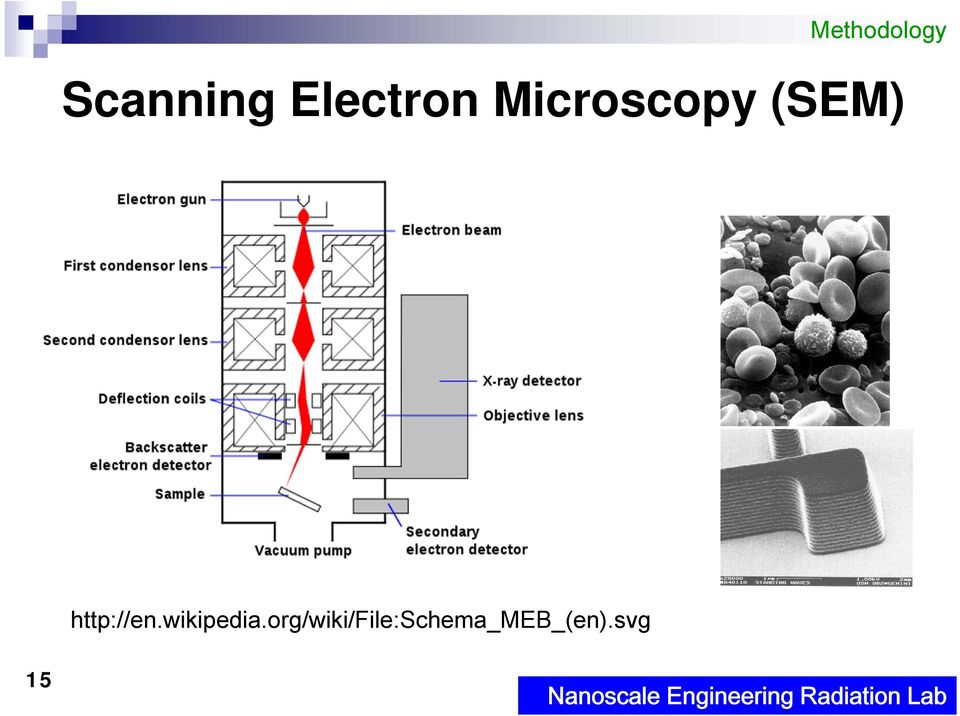
15 Methodology Scanning Electron Microscopy (SEM) 15
16 Methodology Transmission Electron Microscopy (TEM) Transmission electron microscopy (TEM) is a microscopy technique whereby a beam of electrons is transmitted through an ultra thin specimen, interacting with the specimen as it passes through. An image is formed from the interaction of the electrons transmitted through the specimen; the image is magnified and focused onto an imaging device, such as a fluorescent screen, on a layer of photographic film, or to be detected by a sensor such as a CCD camera. 16

17 Scanning Probe Microscopy (SPM) Methodology Scanning probe microscopy (SPM) is a branch of microscopy that forms images of surfaces using a physical probe that scans the specimen. An image of the surface is obtained by mechanically moving the probe in a raster scan of the specimen, line by line, and recording the probe-surface interaction as a function of position. SPM was founded with the invention of the scanning tunneling microscope in The SPM has multiple types, including AFM, NSOM(SNOM), and so on. 17

18 Methodology Atomic Force Microscopy (AFM) The AFM consists of a cantilever with a sharp tip (probe) at its end that is used to scan the specimen surface. The cantilever is typically silicon or silicon nitride with a tip radius of curvature on the order of nanometers. When the tip is brought into proximity of a sample surface, forces between the tip and the sample lead to a deflection of the cantilever according to Hooke's law. Typically, the deflection is measured using a laser spot reflected from the top surface of the cantilever into an array of photodiodes. Other methods that are used include optical interferometry, capacitive sensing or piezoresistive AFM cantilevers. 18

19 Methodology Near-Field Scanning Optical Microscopy (NSOM) 19 Near-field scanning optical microscopy (NSOM/SNOM) is a microscopy technique for nanostructure investigation that breaks the far field resolution limit by exploiting the properties of evanescent waves. This is done by placing the detector very close (distance much smaller than wavelength λ) to the specimen surface. This allows for the surface inspection with high spatial, spectral and temporal resolving power. In particular, lateral resolution of 20 nm and vertical resolution of 2 5 nm have been demonstrated. As in optical microscopy, the contrast mechanism can be easily adapted to study different properties, such as refractive index, chemical structure and local stress.

20 Focused Ion Beam Microscopy (FIB) Methodology Focused ion beam (FIB) systems operate in a similar fashion to a scanning electron microscope (SEM) except, rather than a beam of electrons and as the name implies, FIB systems use a finely focused beam of ions (usually gallium) that can be operated at low beam currents for imaging or high beam currents for site specific sputtering or milling. 20

21 Fabrication of Nanoscale Structures (1/3) 21 Background Fabricating structures at the nano level can be broken down into two main methods; top down and bottom up construction. Top Down Fabrication Top down fabrication can be likened to sculpting from a block of stone. A piece of the base material is gradually eroded until the desired shape is achieved. That is, you start at the top of the blank piece and work your way down removing material from where it is not required. Nanotechnology techniques for top down fabrication vary but can be split into mechanical and chemical fabrication techniques. Top Down Fabrication Techniques The most top down fabrication technique is nanolithography. In this process, required material is protected by a mask and the exposed material is etched away. Depending upon the level of resolution required for features in the final product, etching of the base material can be done chemically using acids or mechanically using ultraviolet light, x-rays or electron beams. This is the technique applied to the manufacture of computer chips. Methodology nomanufacturing.html
22 Methodology Fabrication of Nanoscale Structures (2/3) 22 Bottom Up Fabrication Bottom up fabrication can be likened to building a brick house. Instead of placing bricks one at a time to produce a house, bottom up fabrication techniques place atoms or molecules one at a time to build the desired nanostructure. Such processes are time consuming and so self assembly techniques are employed where the atoms arrange themselves as required. Bottom Up Fabrication Techniques Self assembling nanomachines are regularly mentioned by science fiction writers but significant obstacles including the laws of physics will need to be overcome or circumvented before this becomes a reality. Other areas involving bottom up fabrication are already quite successful. Manufacturing quantum dots by selfassembly quantum dots has rendered the top down lithographic approach to semiconductor quantum dot fabrication virtually obsolete.
23 Methodology Fabrication of Nanoscale Structures (3/3) Advantages Top-down Once Research and Development complete and manufacturing line is complete costs drop Bulk production Bottom-up Self-Assembly processes Less product defects Disadvantages Contamination Machine Cost Complexity Clean room cost and complexity Physical limits Material damage Surface imperfections Heat dissipation Not very robust products Lengthy process to obtain nanoparticles 23
24 Outline Outline History Definition Methodology Applications Challenges, Risks, and Ethics 24
25 Applications Chocolate Self-assembly Making chocolate considered "good" is about forming as many type V crystals as possible. This provides the best appearance and texture and creates the most stable crystals, so the texture and appearance will not degrade over time. To accomplish this, the temperature is carefully manipulated during the crystallization. Crystal Melting temp. Notes I 17 C (63 F) Soft, crumbly, melts too easily II 21 C (70 F) Soft, crumbly, melts too easily III 26 C (79 F) Firm, poor snap, melts too easily IV 28 C (82 F) Firm, good snap, melts too easily V 34 C (93 F) Glossy, firm, best snap, melts near body temperature (37 C) VI 36 C (97 F) Hard, takes weeks to form 25
26 Smart phone Applications A smartphone is a mobile phone built on a mobile computing platform, with more advanced computing ability and connectivity than a feature phone.the first smartphones mainly combined the functions of a personal digital assistant (PDA) and a mobile phone or camera phone. Today's models also serve to combine the functions of portable media players, low-end compact digital cameras, pocket video cameras, and GPS navigation units. Modern smartphones typically also include high-resolution touchscreens, web browsers that can access and properly display standard web pages rather than just mobile-optimized sites, and high-speed data access via Wi-Fi and mobile broadband. 26
27 Applications Cosmetics In cosmetics there are currently two main uses for nanotechnology. The first of these is the use of nanoparticles as UV filters. Titanium dioxide (TiO2) and Zinc oxide (ZnO) are the main compounds used in these applications. Organic alternatives to these have also been developed. The second use is nanotechnology for delivery. Liposomes and niosomes are used in the cosmetic industry as delivery vehicles. Newer structures such as solid lipid nanoparticles (SLN) and nanostructured lipid carriers (NLC) have been found to be better performers than liposomes. In particular, NLCs have been identified as a potential next generation cosmetic delivery agent that can provide enhanced skin hydration, bioavailability, stability of the agent and controlled occlusion. Encapsulation techniques have been proposed for carrying cosmetic actives April%2009.pdf
28 Applications Morpho 28 Many Morpho butterflies are colored in metallic, shimmering shades of blue and green. These colors are an example of iridescence: the microscopic scales covering the Morpho's wings reflect incident light repeatedly at successive layers, leading to interference effects that depend on both wavelength and angle of incidence/observance. Thus the colors produced vary with viewing angle, however they are actually surprisingly uniform, perhaps due to the tetrahedral (diamond-like) structural arrangement of the scales or diffraction from overlying cell layers. This structure may be likened to a photonic crystal. The lamellate structure of their wing scales has been studied as a model in the development of fabrics, dye-free paints, and anti-counterfeit technology used in currency.
29 Applications Carbon Nanotube (CNTs) High tensile strength (~63 GPa) >> High-carbon steel (1.2 GPa) High elastic modulus (~ 1 TPa) High thermal conductivity along the nanotube (6000 W/m/K) >> Copper (385 W/m/K) High electrical current density for armchair nanotubes (~1000 times that of metals) 29
30 Accplications Multifunctional Nanowire Bioscaffolds A simple and inexpensive way to create a nanowire coating on the surface of biocompatible titanium has been developed. The technique could be used to create more effective surfaces for prosthetics, such as hip replacements, as well as in dental reconstruction and vascular stents. The material can also be easily sterilised using ultraviolet light and water or ethanol, which means it could safely be used in hospitals. 30 Chem. Mater. 2007, 19,
31 Applications Moore s Law The number of transistors per square inch on integrated circuits double every year. "..(T)he first microprocessor only had 22 hundred transistors. We are looking at something a million times that complex in the next generations a billion transistors. What that gives us in the way of flexibility to design products is phenomenal." Gordon E. Moore,
32 Applications Lotus Effect The lotus effect refers to the very high water repellence (superhydrophobicity) exhibited by the leaves of the lotus flower (Nelumbo). Dirt particles are picked up by water droplets due to a complex micro- and nanoscopic architecture of the surface, which minimizes adhesion. The hydrophobicity of a surface is related to its contact angle. The higher the contact angle the higher the hydrophobicity of a surface. Surfaces with a contact angle < 90 are referred to as hydrophilic and those with an angle >90 as hydrophobic. Plants with a double structured surface like the lotus can reach a contact angle of 170 whereas a droplet s actual contact area is only 0.6%. All this leads to a self-cleaning effect. 32
33 Applications Fuel Cells Catalysts are used with fuels such as hydrogen or methanol to produce hydrogen ions. Platinum, which is very expensive, is the catalyst typically used in this process. Companies are using nanoparticles of platinum to reduce the amount of platinum needed, or using nanoparticles of other materials to replace platinum entirely and thereby lower costs. Fuel cells contain membranes that allow hydrogen ions to pass through the cell but do not allow other atoms or ions, such as oxygen, to pass through. Companies are using nanotechnology to create more efficient membranes; this will allow them to build lighter weight and longer lasting fuel cells. Researchers at Rensselaer Polytechnic Institute have investigated the storage of hydrogen in graphene (single atom thick carbon sheets). Hydrogen has a high bonding energy to carbon, and the researchers used annealing and plasma treatment to increase this bonding energy. 33
34 Outline Outline History Definition Methodology Applications Challenges, Risks, and Ethics 34
35 Challenges, Risks, and Ethics Challenges, Risks, and Ethics 1. Monitoring the exposure of nanoscale engineered to humans in the air and within water. The challenge becomes increasingly difficult in more complex matrices like food. 2. Developing and validating methods to evaluate the toxicity of engineered nano-materials. 3. Constructing models for predicting the potential impact of engineered nano-materials on the environment and human health. 4. Educating people about the pros and cons for nanotechnology Defining areas applicable to nanotechnology with regulations and laws. Overemphasized functions of nanotechnology should be prohibited.
Usage of Carbon Nanotubes in Scanning Probe Microscopes as Probe. Keywords: Carbon Nanotube, Scanning Probe Microscope
 International Journal of Arts and Sciences 3(1): 18-26 (2009) CD-ROM. ISSN: 1944-6934 InternationalJournal.org Usage of Carbon Nanotubes in Scanning Probe Microscopes as Probe Bedri Onur Kucukyildirim,
Basic principles and mechanisms of NSOM; Different scanning modes and systems of NSOM; General applications and advantages of NSOM.
 Lecture 16: Near-field Scanning Optical Microscopy (NSOM) Background of NSOM; Basic principles and mechanisms of NSOM; Basic components of a NSOM; Different scanning modes and systems of NSOM; General
Nanoscience Course Descriptions
 Nanoscience Course Descriptions NANO*1000 Introduction to Nanoscience This course introduces students to the emerging field of nanoscience. Its representation in popular culture and journalism will be
What is Nanophysics: Survey of Course Topics. Branislav K. Nikolić
 What is Nanophysics: Survey of Course Topics Branislav K. Nikolić Department of Physics and Astronomy, University of Delaware, Newark, DE 19716, U.S.A. http://wiki.physics.udel.edu/phys824 Definition of
Lecture 6 Scanning Tunneling Microscopy (STM) General components of STM; Tunneling current; Feedback system; Tip --- the probe.
 General components of STM; Tunneling current; Feedback system; Tip --- the probe.") Lecture 6 Scanning Tunneling Microscopy (STM) General components of STM; Tunneling current; Feedback system; Tip --- the probe. Brief Overview of STM Inventors of STM The Nobel Prize in Physics 1986 Nobel
Lecture 6 Scanning Tunneling Microscopy (STM) General components of STM; Tunneling current; Feedback system; Tip --- the probe. Brief Overview of STM Inventors of STM The Nobel Prize in Physics 1986 Nobel
5. Scanning Near-Field Optical Microscopy 5.1. Resolution of conventional optical microscopy
 5. Scanning Near-Field Optical Microscopy 5.1. Resolution of conventional optical microscopy Resolution of optical microscope is limited by diffraction. Light going through an aperture makes diffraction
h e l p s y o u C O N T R O L
 contamination analysis for compound semiconductors ANALYTICAL SERVICES B u r i e d d e f e c t s, E v a n s A n a l y t i c a l g r o u p h e l p s y o u C O N T R O L C O N T A M I N A T I O N Contamination
Will nano change my life?
 Nanotechnology is in products you use every day Will nano change my life? Nanotechnology is a new field of science and engineering that focuses on studying and making very, very small things. Nanotechnologies
Nanoelectronics 09. Atsufumi Hirohata Department of Electronics. Quick Review over the Last Lecture
 Nanoelectronics 09 Atsufumi Hirohata Department of Electronics 12:00 Wednesday, 4/February/2015 (P/L 006) Quick Review over the Last Lecture ( Field effect transistor (FET) ): ( Drain ) current increases
Atomic Force Microscopy. Long Phan Nanotechnology Summer Series May 15, 2013
 Atomic Force Microscopy Long Phan Nanotechnology Summer Series May 15, 2013 1 World s Smallest Movie 2 Outline What is AFM? How does AFM Work? 3 Modes: Contact mode Non contact mode Tapping mode Imaging
CS257 Introduction to Nanocomputing
 CS257 Introduction to Nanocomputing Overview of Crossbar-Based Computing John E Savage Overview Intro to NW growth methods Chemical vapor deposition and fluidic assembly Nano imprinting Nano stamping Four
Technology White Papers nr. 13 Paul Holister Cristina Román Vas Tim Harper
 QUANTUM DOTS Technology White Papers nr. 13 Paul Holister Cristina Román Vas Tim Harper QUANTUM DOTS Technology White Papers nr. 13 Release Date: Published by Científica Científica, Ltd. www.cientifica.com
CREOL, College of Optics & Photonics, University of Central Florida
 OSE6650 - Optical Properties of Nanostructured Materials Optical Properties of Nanostructured Materials Fall 2013 Class 3 slide 1 Challenge: excite and detect the near field Thus far: Nanostructured materials
Near-field scanning optical microscopy (SNOM)
") Adviser: dr. Maja Remškar Institut Jožef Stefan January 2010 1 2 3 4 5 6 Fluorescence Raman and surface enhanced Raman 7 Conventional optical microscopy-limited resolution Two broad classes of techniques
Adviser: dr. Maja Remškar Institut Jožef Stefan January 2010 1 2 3 4 5 6 Fluorescence Raman and surface enhanced Raman 7 Conventional optical microscopy-limited resolution Two broad classes of techniques
Conductivity of silicon can be changed several orders of magnitude by introducing impurity atoms in silicon crystal lattice.
 CMOS Processing Technology Silicon: a semiconductor with resistance between that of conductor and an insulator. Conductivity of silicon can be changed several orders of magnitude by introducing impurity
Phase Characterization of TiO 2 Powder by XRD and TEM
 Kasetsart J. (Nat. Sci.) 42 : 357-361 (28) Phase Characterization of TiO 2 Powder by XRD and TEM Kheamrutai Thamaphat 1 *, Pichet Limsuwan 1 and Boonlaer Ngotawornchai 2 ABSTRACT In this study, the commercial
Scanning Near Field Optical Microscopy: Principle, Instrumentation and Applications
 Scanning Near Field Optical Microscopy: Principle, Instrumentation and Applications Saulius Marcinkevičius Optics, ICT, KTH 1 Outline Optical near field. Principle of scanning near field optical microscope
Chemical Synthesis. Overview. Chemical Synthesis of Nanocrystals. Self-Assembly of Nanocrystals. Example: Cu 146 Se 73 (PPh 3 ) 30
 30") Chemical Synthesis Spontaneous organization of molecules into stable, structurally well-defined aggregates at the nanometer length scale. Overview The 1-100 nm nanoscale length is in between traditional
Chemical Synthesis Spontaneous organization of molecules into stable, structurally well-defined aggregates at the nanometer length scale. Overview The 1-100 nm nanoscale length is in between traditional
Microscopy: Principles and Advances
 Microscopy: Principles and Advances Chandrashekhar V. Kulkarni University of Central Lancashire, Preston, United kingdom May, 2014 University of Ljubljana Academic Background 2005-2008: PhD-Chemical Biology
Scanning Probe Microscopy
 Ernst Meyer Hans Josef Hug Roland Bennewitz Scanning Probe Microscopy The Lab on a Tip With 117 Figures Mß Springer Contents 1 Introduction to Scanning Probe Microscopy f f.1 Overview 2 f.2 Basic Concepts
Fundamental Nanomaterials Research and Development: An Australian Perspective
 Fundamental Research and Development: An Australian Perspective Professor Max Lu FTSE, Fed Fellow, Director Http://www.arccfn.org.au Gross Domestic Expenditure on R&D Australia 10000 8000 Business Government
Nanoscale Resolution Options for Optical Localization Techniques. C. Boit TU Berlin Chair of Semiconductor Devices
 berlin Nanoscale Resolution Options for Optical Localization Techniques C. Boit TU Berlin Chair of Semiconductor Devices EUFANET Workshop on Optical Localization Techniques Toulouse, Jan 26, 2009 Jan 26,
www.keithley.com 1 st Edition Nanotechnology Measurement Handbook A Guide to Electrical Measurements for Nanoscience Applications
 www.keithley.com 1 st Edition Nanotechnology Measurement Handbook A Guide to Electrical Measurements for Nanoscience Applications To get a free electronic version of this book, visit Keithley s Knowledge
DNA NANOWIRES USING NANOPARTICLES ECG653 Project Report submitted by GOPI KRISHNA.ARI,[email protected],Fall-2008
 DNA NANOWIRES USING NANOPARTICLES ECG653 Project Report submitted by GOPI KRISHNA.ARI,[email protected],Fall-2008 INTRODUCTION: Deoxyribonucleic acid (DNA) has been a key building block in nanotechnology
Applications and Benefits of Multi-Walled Carbon Nanotubes (MWCNT)
") I Applications and Benefits of Multi-Walled Carbon Nanotubes (MWCNT) Table of Content 1 Introduction...1 2 Improved Properties...1 3 Potential Applications...1 3.1 Current / short-term applications...3
I Applications and Benefits of Multi-Walled Carbon Nanotubes (MWCNT) Table of Content 1 Introduction...1 2 Improved Properties...1 3 Potential Applications...1 3.1 Current / short-term applications...3
Graphene a material for the future
 Graphene a material for the future by Olav Thorsen What is graphene? What is graphene? Simply put, it is a thin layer of pure carbon What is graphene? Simply put, it is a thin layer of pure carbon It has
Nanoparticle Deposition on Packaging Materials by the Liquid Flame Spray
 Nanoparticle Deposition on Packaging Materials by the Liquid Flame Spray Hannu Teisala a, Mikko Tuominen a, Mikko Aromaa b, Jyrki M. Mäkelä b, Milena Stepien c, Jarkko J. Saarinen c, Martti Toivakka c
Lecture 4 Scanning Probe Microscopy (SPM)
") Lecture 4 Scanning Probe Microscopy (SPM) General components of SPM; Tip --- the probe; Cantilever --- the indicator of the tip; Tip-sample interaction --- the feedback system; Scanner --- piezoelectric
Lecture 4 Scanning Probe Microscopy (SPM) General components of SPM; Tip --- the probe; Cantilever --- the indicator of the tip; Tip-sample interaction --- the feedback system; Scanner --- piezoelectric
Nanocomputer & Architecture
 Nanocomputer & Architecture Yingjie Wei Western Michigan University Department of Computer Science CS 603 - Dr. Elise dedonckor Febrary 4 th, 2004 Nanocomputer Architecture Contents Overview of Nanotechnology
It has long been a goal to achieve higher spatial resolution in optical imaging and
 Nano-optical Imaging using Scattering Scanning Near-field Optical Microscopy Fehmi Yasin, Advisor: Dr. Markus Raschke, Post-doc: Dr. Gregory Andreev, Graduate Student: Benjamin Pollard Department of Physics,
3D TOPOGRAPHY & IMAGE OVERLAY OF PRINTED CIRCUIT BOARD ASSEMBLY
 3D TOPOGRAPHY & IMAGE OVERLAY OF PRINTED CIRCUIT BOARD ASSEMBLY Prepared by Duanjie Li, PhD & Andrea Novitsky 6 Morgan, Ste156, Irvine CA 92618 P: 949.461.9292 F: 949.461.9232 nanovea.com Today's standard
PHYSICAL METHODS, INSTRUMENTS AND MEASUREMENTS Vol. IV Femtosecond Measurements Combined With Near-Field Optical Microscopy - Artyom A.
 FEMTOSECOND MEASUREMENTS COMBINED WITH NEAR FIELD OPTICAL MICROSCOPY Artyom A. Astafiev, Semyonov Institute of Chemical Physics, Moscow, Russian Federation. Keywords: diffraction limit nearfield scanning
Computational Nanoscience of Soft Matter
 ChE/MSE 557 Computational Nanoscience of Soft Matter Fall 2006 Instructor: Professor Sharon C. Glotzer Class meets: Tues 3:00-6:00 Location: Room 3336 BD, Duderstadt Center Room 3336 AC, Duderstadt Center
Microscopy. MICROSCOPY Light Electron Tunnelling Atomic Force RESOLVE: => INCREASE CONTRAST BIODIVERSITY I BIOL1051 MAJOR FUNCTIONS OF MICROSCOPES
 BIODIVERSITY I BIOL1051 Microscopy Professor Marc C. Lavoie [email protected] MAJOR FUNCTIONS OF MICROSCOPES MAGNIFY RESOLVE: => INCREASE CONTRAST Microscopy 1. Eyepieces 2. Diopter adjustment
Modification of Graphene Films by Laser-Generated High Energy Particles
 Modification of Graphene Films by Laser-Generated High Energy Particles Elena Stolyarova (Polyakova), Ph.D. ATF Program Advisory and ATF Users Meeting April 2-3, 2009, Berkner Hall, Room B, BNL Department
Nano-Spectroscopy. Solutions AFM-Raman, TERS, NSOM Chemical imaging at the nanoscale
 Nano-Spectroscopy Solutions AFM-Raman, TERS, NSOM Chemical imaging at the nanoscale Since its introduction in the early 80 s, Scanning Probe Microscopy (SPM) has quickly made nanoscale imaging an affordable
Highlights of Solid State Physics. Man of the Year Nobel Prizes
 Highlights of Solid State Physics Man of the Year Nobel Prizes Silicon Technology Moore s Law Gordon Moore Intel Jack Kilby 14 nm 2014 Physics Nobel Prize 2000 Integrated Circuit Electrons in the Conduction
Physics 441/2: Transmission Electron Microscope
 Physics 441/2: Transmission Electron Microscope Introduction In this experiment we will explore the use of transmission electron microscopy (TEM) to take us into the world of ultrasmall structures. This
Implementation Of High-k/Metal Gates In High-Volume Manufacturing
 White Paper Implementation Of High-k/Metal Gates In High-Volume Manufacturing INTRODUCTION There have been significant breakthroughs in IC technology in the past decade. The upper interconnect layers of
JOURNAL INTEGRATED CIRCUITS AND SYSTEMS, VOL 1, NO. 3, JULY 2006. 39
 JOURNAL INTEGRATED CIRCUITS AND SYSTEMS, VOL 1, NO. 3, JULY 2006. 39 Self-Assembled Polystyrene Micro-Spheres Applied for Photonic Crystals and Templates Fabrication Daniel S. Raimundo 1, Francisco J.
Demonstration of sub-4 nm nanoimprint lithography using a template fabricated by helium ion beam lithography
 Demonstration of sub-4 nm nanoimprint lithography using a template fabricated by helium ion beam lithography Wen-Di Li*, Wei Wu** and R. Stanley Williams Hewlett-Packard Labs *Current address: University
Nanotechnology and Its Impact on Modern Computer
 Global Journal of Researches in Engineering General Engineering Volume 12 Issue 4 Version 1.0 Year 2012 Type: Double Blind Peer Reviewed International Research Journal Publisher: Global Journals Inc. (USA)
Nanometer-scale imaging and metrology, nano-fabrication with the Orion Helium Ion Microscope
 [email protected] Nanometer-scale imaging and metrology, nano-fabrication with the Orion Helium Ion Microscope Bin Ming, András E. Vladár and Michael T. Postek National Institute of Standards and Technology
CSCI 4974 / 6974 Hardware Reverse Engineering. Lecture 8: Microscopy and Imaging
 CSCI 4974 / 6974 Hardware Reverse Engineering Lecture 8: Microscopy and Imaging Data Acquisition for RE Microscopy Imaging Registration and stitching Microscopy Optical Electron Scanning Transmission Scanning
for Low power Energy Harvesting Sun to fiber' Solar Devices
 Nanostructured Energy Conversion for Low power Energy Harvesting Devices and Beyond for High power Sun to fiber' Solar Devices Michael Oye and Nobuhiko Nobby Kobayashi Advanced Studies Laboratories and
Overview. What is EMR? Electromagnetic Radiation (EMR) LA502 Special Studies Remote Sensing
 LA502 Special Studies Remote Sensing") LA502 Special Studies Remote Sensing Electromagnetic Radiation (EMR) Dr. Ragab Khalil Department of Landscape Architecture Faculty of Environmental Design King AbdulAziz University Room 103 Overview What
LA502 Special Studies Remote Sensing Electromagnetic Radiation (EMR) Dr. Ragab Khalil Department of Landscape Architecture Faculty of Environmental Design King AbdulAziz University Room 103 Overview What
Graphical displays are generally of two types: vector displays and raster displays. Vector displays
 Display technology Graphical displays are generally of two types: vector displays and raster displays. Vector displays Vector displays generally display lines, specified by their endpoints. Vector display
GREEN NANOTECHNOLOGY. Geoffrey. Energy in the Built Environment. Solutions for Sustainability and. B. Smith Claes G. Granqvist.
 GREEN NANOTECHNOLOGY Solutions for Sustainability and Energy in the Built Environment Geoffrey B. Smith Claes G. Granqvist CRC Press Taylor & Francis Group Boca Raton London NewYork CRC Press is an imprint
Size effects. Lecture 6 OUTLINE
 Size effects 1 MTX9100 Nanomaterials Lecture 6 OUTLINE -Why does size influence the material s properties? -How does size influence the material s performance? -Why are properties of nanoscale objects
Atomic Force Microscopy Observation and Characterization of a CD Stamper, Lycopodium Spores, and Step-Height Standard Diffraction Grating
 Atomic Force Microscopy Observation and Characterization of a CD Stamper, Lycopodium Spores, and Step-Height Standard Diffraction Grating Michael McMearty and Frit Miot Special Thanks to Brendan Cross
- particle with kinetic energy E strikes a barrier with height U 0 > E and width L. - classically the particle cannot overcome the barrier
 Tunnel Effect: - particle with kinetic energy E strikes a barrier with height U 0 > E and width L - classically the particle cannot overcome the barrier - quantum mechanically the particle can penetrated
Scanning Near-Field Optical Microscopy for Measuring Materials Properties at the Nanoscale
 Scanning Near-Field Optical Microscopy for Measuring Materials Properties at the Nanoscale Outline Background Research Design Detection of Near-Field Signal Submonolayer Chemical Sensitivity Conclusions
Chapter 4. Microscopy, Staining, and Classification. Lecture prepared by Mindy Miller-Kittrell North Carolina State University
 Chapter 4 Microscopy, Staining, and Classification 2012 Pearson Education Inc. Lecture prepared by Mindy Miller-Kittrell North Carolina State University Microscopy and Staining 2012 Pearson Education Inc.
Scanning probe microscopy AFM, STM. Near field Scanning Optical Microscopy(NSOM) Scanning probe fabrication
 Scanning probe fabrication") Scanning probe microscopy AFM, STM Near field Scanning Optical Microscopy(NSOM) Scanning probe fabrication Scanning Probe Microscopy 1986 Binning and Rohrer shared Nobel Prize in Physics for invention.stm
Scanning probe microscopy AFM, STM Near field Scanning Optical Microscopy(NSOM) Scanning probe fabrication Scanning Probe Microscopy 1986 Binning and Rohrer shared Nobel Prize in Physics for invention.stm
How to Build a Printed Circuit Board. Advanced Circuits Inc 2004
 How to Build a Printed Circuit Board 1 This presentation is a work in progress. As methods and processes change it will be updated accordingly. It is intended only as an introduction to the production
Nanotechnology for Food Processing and Packaging
 Nanotechnology for Food Processing and Packaging John D. Floros Professor & Head Department of Food Science Pennsylvania State University www.foodscience.psu.edu Information Sources Pennsylvania State
Unit 12 Practice Test
 Name: Class: Date: ID: A Unit 12 Practice Test Multiple Choice Identify the choice that best completes the statement or answers the question. 1) A solid has a very high melting point, great hardness, and
Novel inkjettable copper ink utilizing processing temperatures under 100 degrees C without the need of inert atmosphere
 Novel inkjettable copper ink utilizing processing temperatures under 100 degrees C without the need of inert atmosphere Printed Electronics Europe April 7-8, 2009 Dresden, Germany Dr. Zvi Yaniv Applied
Scanning Electron Microscopy Services for Pharmaceutical Manufacturers
 Scanning Electron Microscopy Services for Pharmaceutical Manufacturers Author: Gary Brake, Marketing Manager Date: August 1, 2013 Analytical Testing Laboratory www.atl.semtechsolutions.com Scanning Electron
Nano Technology for Computer Science: Scope and Opportunities
 International Journal of Electronic and Electrical Engineering. ISSN 0974-2174, Volume 7, Number 3 (2014), pp. 213-218 International Research Publication House http://www.irphouse.com Nano Technology for
From Nano-Electronics and Photonics to Renewable Energy
 From Nano-Electronics and Photonics to Renewable Energy Tom Smy Department of Electronics, Carleton University Questions are welcome! OUTLINE Introduction: to EE and Engineering Physics Renewable Energy
Keysight Technologies How to Choose your MAC Lever. Technical Overview
 Keysight Technologies How to Choose your MAC Lever Technical Overview Introduction Atomic force microscopy (AFM) is a sub-nanometer scale imaging and measurement tool that can be used to determine a sample
Le nanotecnologie: dal Laboratorio al Mercato. Fabrizio Pirri Politecnico di Torino Istituto Italiano di Tecnologia
 Le nanotecnologie: dal Laboratorio al Mercato Fabrizio Pirri Politecnico di Torino Istituto Italiano di Tecnologia Materials & Processes for micro nanotechnologies Laboratory http://www.polito.it/micronanotech
Pulsed laser deposition of organic materials
 Pulsed laser deposition of organic materials PhD theses Gabriella Kecskeméti Department of Optics and Quantum Electronics University of Szeged Supervisor: Dr. Béla Hopp senior research fellow Department
SOLAR CELLS From light to electricity
 SOLAR CELLS From light to electricity Solar Impulse uses nothing but light to power its motors. The effect of light on the material in solar panels allows them to produce the electricity that is needed
1 Introduction. 1.1 Historical Perspective
 j1 1 Introduction 1.1 Historical Perspective The invention of scanning probe microscopy is considered one of the major advances in materials science since 1950 [1, 2]. Scanning probe microscopy includes
11. Current and potential commercial nanotechnology 4applications
 11. Current and potential commercial nanotechnology 4applications The market for nanotechnology products is already huge and is predicted to grow rapidly in the coming years. This topic guide examines
3D Raman Imaging Nearfield-Raman TERS. Solutions for High-Resolution Confocal Raman Microscopy. www.witec.de
 3D Raman Imaging Nearfield-Raman TERS Solutions for High-Resolution Confocal Raman Microscopy www.witec.de 01 3D Confocal Raman Imaging Outstanding performance in speed, sensitivity, and resolution with
Laser Based Micro and Nanoscale Manufacturing and Materials Processing
 Laser Based Micro and Nanoscale Manufacturing and Materials Processing Faculty: Prof. Xianfan Xu Email: [email protected] Phone: (765) 494-5639 http://widget.ecn.purdue.edu/~xxu Research Areas: Development
OPTIMIZING OF THERMAL EVAPORATION PROCESS COMPARED TO MAGNETRON SPUTTERING FOR FABRICATION OF TITANIA QUANTUM DOTS
 OPTIMIZING OF THERMAL EVAPORATION PROCESS COMPARED TO MAGNETRON SPUTTERING FOR FABRICATION OF TITANIA QUANTUM DOTS Vojtěch SVATOŠ 1, Jana DRBOHLAVOVÁ 1, Marian MÁRIK 1, Jan PEKÁREK 1, Jana CHOMOCKÁ 1,
P R E A M B L E. Facilitated workshop problems for class discussion (1.5 hours)
") INSURANCE SCAM OPTICS - LABORATORY INVESTIGATION P R E A M B L E The original form of the problem is an Experimental Group Research Project, undertaken by students organised into small groups working as
INSURANCE SCAM OPTICS - LABORATORY INVESTIGATION P R E A M B L E The original form of the problem is an Experimental Group Research Project, undertaken by students organised into small groups working as
Use the BET (after Brunauer, Emmett and Teller) equation is used to give specific surface area from the adsorption
 equation is used to give specific surface area from the adsorption") Number of moles of N 2 in 0.129dm 3 = 0.129/22.4 = 5.76 X 10⁻³ moles of N 2 gas Module 8 : Surface Chemistry Objectives Lecture 37 : Surface Characterization Techniques After studying this lecture, you
Number of moles of N 2 in 0.129dm 3 = 0.129/22.4 = 5.76 X 10⁻³ moles of N 2 gas Module 8 : Surface Chemistry Objectives Lecture 37 : Surface Characterization Techniques After studying this lecture, you
NANOSCALE SCIENCE AND ENGINEERING: MATERIALS, ELECTRONICS, PHOTONICS, BIOSENSORS AND BEYOND
 Inversion mode MOSFET p- pn junction Silicon film (n- type) Gate Silicon film (p- type) Gate oxide Continuing Education Program (CEP) on NANOSCALE SCIENCE AND ENGINEERING: MATERIALS, ELECTRONICS, PHOTONICS,
Single Defect Center Scanning Near-Field Optical Microscopy on Graphene
 1 2 3 4 5 6 7 8 9 10 11 12 13 14 15 16 17 Single Defect Center Scanning Near-Field Optical Microscopy on Graphene J. Tisler, T. Oeckinghaus, R. Stöhr, R. Kolesov, F. Reinhard and J. Wrachtrup 3. Institute
NANOTECHNOLOGY BACKGROUND
 NANOTECHNOLOGY BACKGROUND Introduction and Overview Nanotechnology is defined as the study of the fundamental laws and theories of atoms and structures that have critical dimensions between 1 and 100 nanometers.
PHYS 222 Spring 2012 Final Exam. Closed books, notes, etc. No electronic device except a calculator.
 PHYS 222 Spring 2012 Final Exam Closed books, notes, etc. No electronic device except a calculator. NAME: (all questions with equal weight) 1. If the distance between two point charges is tripled, the
Electron Microscopy 3. SEM. Image formation, detection, resolution, signal to noise ratio, interaction volume, contrasts
 Electron Microscopy 3. SEM Image formation, detection, resolution, signal to noise ratio, interaction volume, contrasts 3-1 SEM is easy! Just focus and shoot "Photo"!!! Please comment this picture... Any
LabRAM HR. Research Raman Made Easy! Raman Spectroscopy Systems. Spectroscopy Suite. Powered by:
 LabRAM HR Research Raman Made Easy! Raman Spectroscopy Systems Powered by: Spectroscopy Suite Cutting-Edge Applications with the LabRAM HR Deeply involved in Raman spectroscopy for decades, HORIBA Scientific
NEAR FIELD OPTICAL MICROSCOPY AND SPECTROSCOPY WITH STM AND AFM PROBES
 Vol. 93 (1997) A CTA PHYSICA POLONICA A No. 2 Proceedings of the 1st International Symposium on Scanning Probe Spectroscopy and Related Methods, Poznań 1997 NEAR FIELD OPTICAL MICROSCOPY AND SPECTROSCOPY
Coating Technology: Evaporation Vs Sputtering
 Satisloh Italy S.r.l. Coating Technology: Evaporation Vs Sputtering Gianni Monaco, PhD R&D project manager, Satisloh Italy 04.04.2016 V1 The aim of this document is to provide basic technical information
Lenses and Apertures of A TEM
 Instructor: Dr. C.Wang EMA 6518 Course Presentation Lenses and Apertures of A TEM Group Member: Anup Kr. Keshri Srikanth Korla Sushma Amruthaluri Venkata Pasumarthi Xudong Chen Outline Electron Optics
Supporting Information
 Supporting Information Simple and Rapid Synthesis of Ultrathin Gold Nanowires, Their Self-Assembly and Application in Surface-Enhanced Raman Scattering Huajun Feng, a Yanmei Yang, a Yumeng You, b Gongping
Sensors & Instruments for station. returned samples. Chun Chia Tan
 Sensors & Instruments for station based materials characterization of returned samples Chun Chia Tan 04/01/2009 Outline Introduction to materials characterization General overview of the equipment used
STM and AFM Tutorial. Katie Mitchell January 20, 2010
 STM and AFM Tutorial Katie Mitchell January 20, 2010 Overview Scanning Probe Microscopes Scanning Tunneling Microscopy (STM) Atomic Force Microscopy (AFM) Contact AFM Non-contact AFM RHK UHV350 AFM/STM
Matter, Materials, Crystal Structure and Bonding. Chris J. Pickard
 Matter, Materials, Crystal Structure and Bonding Chris J. Pickard Why should a theorist care? Where the atoms are determines what they do Where the atoms can be determines what we can do Overview of Structure
Ion Beam Sputtering: Practical Applications to Electron Microscopy
 Ion Beam Sputtering: Practical Applications to Electron Microscopy Applications Laboratory Report Introduction Electron microscope specimens, both scanning (SEM) and transmission (TEM), often require a
Applying NiTi Shape-Memory Thin Films to Thermomechanical Data Storage Technology
 Mater. Res. Soc. Symp. Proc. Vol. 855E 2005 Materials Research Society W1.7.1 Applying NiTi Shape-Memory Thin Films to Thermomechanical Data Storage Technology Wendy C. Crone 1, Gordon A. Shaw 2 1 Department
Physical Properties and Functionalization of Low-Dimensional Materials
 Physical Properties and Functionalization of Low-Dimensional Materials Physics Department, University of Trieste Graduate School of Physics, XXVI cycle Supervisor: Co-supervisor: Prof. Alessandro BARALDI
1. Photon Beam Damage and Charging at Solid Surfaces John H. Thomas III
 1. Photon Beam Damage and Charging at Solid Surfaces John H. Thomas III 1. Introduction............................. 2. Electrostatic Charging of Samples in Photoemission Experiments............................
PLASMA TECHNOLOGY OVERVIEW
 PLASMA TECHNOLOGY OVERVIEW Plasmas are not a lab curiosity. Plasma processing has been an essential production tool for more than 30 years in the fabrication of microelectronic devices for example. Over
Introducing Nanoscience to High School Students
 Introducing Nanoscience to High School Students www.crann.tcd.ie As a Partner of Trinity College. NEATEC is authorized to use and distribute this module to Non-Profit Organizations. This project is sponsored
UNIT I: INTRFERENCE & DIFFRACTION Div. B Div. D Div. F INTRFERENCE
 107002: EngineeringPhysics Teaching Scheme: Lectures: 4 Hrs/week Practicals-2 Hrs./week T.W.-25 marks Examination Scheme: Paper-50 marks (2 hrs) Online -50marks Prerequisite: Basics till 12 th Standard
Focused Ion beam nanopatterning: potential application in photovoltaics
 Focused Ion beam nanopatterning: potential application in photovoltaics Research Infrastructure: Location: FIB-Focused Ion Beam ENEA Portici (Italy) Date March, 26 2013 Speakers: Vera La Ferrara, ENEA
Lapping and Polishing Basics
 Lapping and Polishing Basics Applications Laboratory Report 54 Lapping and Polishing 1.0: Introduction Lapping and polishing is a process by which material is precisely removed from a workpiece (or specimen)
Subject Area(s) Biology. Associated Unit Engineering Nature: DNA Visualization and Manipulation. Associated Lesson Imaging the DNA Structure
 Biology. Associated Unit Engineering Nature: DNA Visualization and Manipulation. Associated Lesson Imaging the DNA Structure") Subject Area(s) Biology Associated Unit Engineering Nature: DNA Visualization and Manipulation Associated Lesson Imaging the DNA Structure Activity Title Inside the DNA Header Image 1 ADA Description:
Subject Area(s) Biology Associated Unit Engineering Nature: DNA Visualization and Manipulation Associated Lesson Imaging the DNA Structure Activity Title Inside the DNA Header Image 1 ADA Description:
20.309: Biological Instrumentation and Measurement. Heejin Choi Rumi Chunara Yuri Matsumoto
 20.309: Biological Instrumentation and Measurement Instructors: Laboratory Instructor: Teaching Assistants: Scott Manalis and Peter So Steve Wasserman Jaewon Cha Heejin Choi Rumi Chunara Yuri Matsumoto
Lecture 20: Scanning Confocal Microscopy (SCM) Rationale for SCM. Principles and major components of SCM. Advantages and major applications of SCM.
 Rationale for SCM. Principles and major components of SCM. Advantages and major applications of SCM.") Lecture 20: Scanning Confocal Microscopy (SCM) Rationale for SCM. Principles and major components of SCM. Advantages and major applications of SCM. Some limitations (disadvantages) of NSOM A trade-off
Lecture 20: Scanning Confocal Microscopy (SCM) Rationale for SCM. Principles and major components of SCM. Advantages and major applications of SCM. Some limitations (disadvantages) of NSOM A trade-off