CD4013BC Dual D-Type Flip-Flop
|
|
|
- Cordelia Allen
- 9 years ago
- Views:
Transcription
1 Dual D-Type Flip-Flop General Description The CD4013B dual D-type flip-flop is a monolithic complementary MOS (CMOS) integrated circuit cotructed with N- and P-channel enhancement mode traistors. Each flip-flop has independent data, set, reset, and clock inputs and Q and Q outputs. These devices can be used for shift register applicatio, and by connecting Q output to the data input, for counter and toggle applicatio. The logic level present at the D input is traferred to the Q output during the positive-going traition of the clock pulse. Setting or resetting is independent of the clock and is accomplished by a high level on the set or reset line respectively. Features October 1987 Revised March 2002 Wide supply voltage range: 3.0 to 15 High noise immunity: 0.45 DD (typ.) Low power TTL: fan out of 2 driving 74L compatibility: or 1 driving 74LS Applicatio Automotive Data terminals Itrumentation Medical electronics Alarm system Industrial electronics Remote metering Computers CD4013BC Dual D-Type Flip-Flop Ordering Code: Order Number Package Number Package Description CD4013BCM M14A 14-Lead Small Outline Integrated Circuit (SOIC), JEDEC MS-012, 0.150" Narrow CD4013BCSJ M14D 14-Lead Small Outline Package (SOP), EIAJ TYPE II, 5.3mm Wide CD4013BCN N14A 14-Lead Plastic Dual-In-Line Package (PDIP), JEDEC MS-001, 0.300" Wide Devices also available in Tape and Reel. Specify by appending the suffix letter X to the ordering code. Connection Diagram Truth Table Top iew CL (Note 1) No Change x = Don't Care Case Note 1: Level Change D R S Q Q x 0 0 Q Q x x x x x x Fairchild Semiconductor Corporation DS

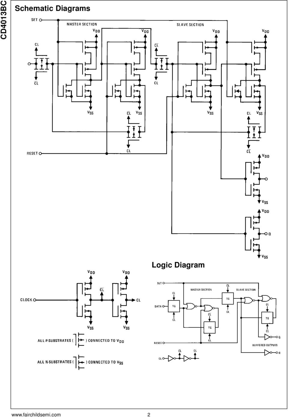
2 Schematic Diagrams Logic Diagram 2
3 Absolute Maximum Ratings(Note 2) (Note 3) DC Supply oltage ( DD ) 0.5 DC to +18 DC Input oltage ( IN ) 0.5 DC to DD +0.5 DC Storage Temperature Range (T S ) 65 C to +150 C Power Dissipation (P D ) Dual-In-Line 700 mw Small Outline 500 mw Lead Temperature (T L ) (Soldering, 10 seconds) 260 C Recommended Operating Conditio (Note 3) DC Supply oltage ( DD ) +3 DC to +15 DC Input oltage ( IN ) 0 DC to DD DC Operating Temperature Range (T A ) 55 C to +125 C Note 2: Absolute Maximum Ratings are those values beyond which the safety of the device cannot be guaranteed, they are not meant to imply that the devices should be operated at these limits. The tables of Recommended Operating Conditio and Electrical Characteristics provide conditio for actual device operation. Note 3: SS = 0 unless otherwise specified. CD4013BC DC Electrical Characteristics (Note 3) Symbol Parameter Conditio 55 C +25 C +125 C Min Max Min Typ Max Min Max I DD Quiescent Device DD = 5, IN = DD or SS Current DD = 10, IN = DD or SS DD = 15, IN = DD or SS OL LOW Level I O < 1.0 µa Output oltage DD = DD = DD = OH HIGH Level I O < 1.0 µa Output oltage DD = DD = DD = IL LOW Level I O < 1.0 µa Input oltage DD = 5, O = 0.5 or DD = 10, O = 1.0 or DD = 15, O = 1.5 or IH HIGH Level I O < 1.0 µa Input oltage DD = 5, O = 0.5 or DD = 10, O = 1.0 or DD = 15, O = 1.5 or I OL LOW Level Output DD = 5, O = Current (Note 4) DD = 10, O = DD = 15, O = I OH HIGH Level Output DD = 5, O = Current (Note 4) DD = 10, O = DD = 15, O = I IN Input Current DD = 15, IN = DD = 15, IN = Note 4: I OH and I OL are measured one output at a time. Units µa ma ma µa 3

4 AC Electrical Characteristics (Note 5) T A = 25 C, C L = 50 pf, R L = 200k, unless otherwise noted Symbol Parameter Conditio Min Typ Max Units CLOCK OPERATION t PHL, t PLH Propagation Delay Time DD = DD = DD = t THL, t TLH Traition Time DD = DD = DD = t WL, t WH Minimum Clock DD = Pulse Width DD = DD = t RCL, t FCL Maximum Clock Rise and DD = 5 15 Fall Time DD = µs DD = 15 5 t SU Minimum Set-Up Time DD = DD = DD = f CL Maximum Clock DD = Frequency DD = MHz DD = SET AND RESET OPERATION t PHL(R), Propagation Delay Time DD = t PLH(S) DD = DD = t WH(R), Minimum Set and DD = t WH(S) Reset Pulse Width DD = DD = C IN Average Input Capacitance Any Input pf Note 5: AC Parameters are guaranteed by DC correlated testing. Switching Time Waveforms 4

5 Physical Dimeio inches (millimeters) unless otherwise noted CD4013BC 14-Lead Small Outline Integrated Circuit (SOIC), JEDEC MS-012, 0.150" Narrow Package Number M14A 5

6 Physical Dimeio inches (millimeters) unless otherwise noted (Continued) 14-Lead Small Outline Package (SOP), EIAJ TYPE II, 5.3mm Wide Package Number M14D 6

7 Physical Dimeio inches (millimeters) unless otherwise noted (Continued) CD4013BC Dual D-Type Flip-Flop 14-Lead Plastic Dual-In-Line Package (PDIP), JEDEC MS-001, 0.300" Wide Package Number N14A Fairchild does not assume any respoibility for use of any circuitry described, no circuit patent licees are implied and Fairchild reserves the right at any time without notice to change said circuitry and specificatio. LIFE SUPPORT POLICY FAIRCHILD S PRODUCTS ARE NOT AUTHORIZED FOR USE AS CRITICAL COMPONENTS IN LIFE SUPPORT DEICES OR SYSTEMS WITHOUT THE EXPRESS WRITTEN APPROAL OF THE PRESIDENT OF FAIRCHILD SEMICONDUCTOR CORPORATION. As used herein: 1. Life support devices or systems are devices or systems which, (a) are intended for surgical implant into the body, or (b) support or sustain life, and (c) whose failure to perform when properly used in accordance with itructio for use provided in the labeling, can be reasonably expected to result in a significant injury to the user. 2. A critical component in any component of a life support device or system whose failure to perform can be reasonably expected to cause the failure of the life support device or system, or to affect its safety or effectiveness

CD4013BC Dual D-Type Flip-Flop
 CD4013BC Dual D-Type Flip-Flop General Description The CD4013B dual D-type flip-flop is a monolithic complementary MOS (CMOS) integrated circuit constructed with N- and P-channel enhancement mode transistors.
CD4027BC Dual J-K Master/Slave Flip-Flop with Set and Reset
 October 1987 Revised March 2002 CD4027BC Dual J-K Master/Slave Flip-Flop with Set and Reset General Description The CD4027BC dual J-K flip-flops are monolithic complementary MOS (CMOS) integrated circuits
CD4001BC/CD4011BC Quad 2-Input NOR Buffered B Series Gate Quad 2-Input NAND Buffered B Series Gate
 Quad 2-Input NOR Buffered B Series Gate Quad 2-Input NAND Buffered B Series Gate General Description The CD4001BC and CD4011BC quad gates are monolithic complementary MOS (CMOS) integrated circuits cotructed
MM74C74 Dual D-Type Flip-Flop
 Dual D-Type Flip-Flop General Description The MM74C74 dual D-type flip-flop is a monolithic complementary MOS (CMOS) integrated circuit cotructed with N- and P-channel enhancement traistors. Each flip-flop
CD40174BC CD40175BC Hex D-Type Flip-Flop Quad D-Type Flip-Flop
 Hex D-Type Flip-Flop Quad D-Type Flip-Flop General Description The CD40174BC consists of six positive-edge triggered D- type flip-flops; the true outputs from each flip-flop are externally available. The
CD4001BC/CD4011BC Quad 2-Input NOR Buffered B Series Gate Quad 2-Input NAND Buffered B Series Gate
 CD4001BC/CD4011BC Quad 2-Input NOR Buffered B Series Gate Quad 2-Input NAND Buffered B Series Gate General Description The CD4001BC and CD4011BC quad gates are monolithic complementary MOS (CMOS) integrated
74F74 Dual D-Type Positive Edge-Triggered Flip-Flop
 Dual D-Type Positive Edge-Triggered Flip-Flop General Description The F74 is a dual D-type flip-flop with Direct Clear and Set inputs and complementary (Q, Q) outputs. Information at the input is traferred
CD4043BC CD4044BC Quad 3-STATE NOR R/S Latches Quad 3-STATE NAND R/S Latches
 CD4043BC CD4044BC Quad 3-STATE NOR R/S Latches Quad 3-STATE NAND R/S Latches General Description The CD4043BC are quad cross-couple 3-STATE CMOS NOR latches, and the CD4044BC are quad cross-couple 3- STATE
MM74HC273 Octal D-Type Flip-Flops with Clear
 MM74HC273 Octal D-Type Flip-Flops with Clear General Description The MM74HC273 edge triggered flip-flops utilize advanced silicon-gate CMOS technology to implement D-type flipflops. They possess high noise
74VHC574 Octal D-Type Flip-Flop with 3-STATE Outputs
 74HC574 Octal D-Type Flip-Flop with 3-STATE Outputs General Description Ordering Code: March 1993 Revised May 2005 The HC574 is an advanced high speed CMOS octal flipflop with 3-STATE output fabricated
MM74HC174 Hex D-Type Flip-Flops with Clear
 Hex D-Type Flip-Flops with Clear General Description The MM74HC174 edge triggered flip-flops utilize advanced silicon-gate CMOS technology to implement D-type flipflops. They possess high noise immunity,
DM7474 Dual Positive-Edge-Triggered D-Type Flip-Flops with Preset, Clear and Complementary Outputs
 DM7474 Dual Positive-Edge-Triggered D-Type Flip-Flops with Preset, Clear and Complementary Outputs General Description This device contains two independent positive-edge-triggered D-type flip-flops with
CD4027BM CD4027BC Dual J-K Master Slave Flip-Flop with Set and Reset
 CD4027BM CD4027BC Dual J-K Master Slave Flip-Flop with Set and Reset General Description These dual J-K flip-flops are monolithic complementary MOS (CMOS) integrated circuits constructed with N- and P-
1-800-831-4242
 Distributed by: www.jameco.com 1-800-831-4242 The content and copyrights of the attached material are the property of its owner. DM74LS161A DM74LS163A Synchronous 4-Bit Binary Counters General Description
DM74LS151 1-of-8 Line Data Selector/Multiplexer
 1-of-8 Line Data Selector/Multiplexer General Description This data selector/multiplexer contains full on-chip decoding to select the desired data source. The DM74LS151 selects one-of-eight data sources.
MM74HCT373 MM74HCT374 3-STATE Octal D-Type Latch 3-STATE Octal D-Type Flip-Flop
 3-STATE Octal D-Type Latch 3-STATE Octal D-Type Flip-Flop General Description The MM74HCT373 octal D-type latches and MM74HCT374 Octal D-type flip flops advanced silicongate CMOS technology, which provides
74AC191 Up/Down Counter with Preset and Ripple Clock
 74AC191 Up/Down Counter with Preset and Ripple Clock General Description The AC191 is a reversible modulo 16 binary counter. It features synchronous counting and asynchronous presetting. The preset feature
MM74C150 MM82C19 16-Line to 1-Line Multiplexer 3-STATE 16-Line to 1-Line Multiplexer
 MM74C150 MM82C19 16-Line to 1-Line Multiplexer 3-STATE 16-Line to 1-Line Multiplexer General Description The MM74C150 and MM82C19 multiplex 16 digital lines to 1 output. A 4-bit address code determines
CD4040BC, 12-Stage Ripple Carry Binary Counters CD4060BC, 14-Stage Ripple Carry Binary Counters
 CD4040BC, 12-Stage Ripple Carry Binary Counters CD4060BC, 14-Stage Ripple Carry Binary Counters Features Wide supply voltage range: 3.0V to 15V High noise immunity: 0.45 V DD (Typ.) Low power TTL compatibility:
MM74HC14 Hex Inverting Schmitt Trigger
 MM74HC14 Hex Inverting Schmitt Trigger General Description The MM74HC14 utilizes advanced silicon-gate CMOS technology to achieve the low power dissipation and high noise immunity of standard CMOS, as
DM74LS00 Quad 2-Input NAND Gate
 DM74LS00 Quad 2-Input NAND Gate General Description This device contains four independent gates each of which performs the logic NAND function. Ordering Code: August 1986 Revised March 2000 Order Number
DM74LS05 Hex Inverters with Open-Collector Outputs
 Hex Inverters with Open-Collector Outputs General Description This device contains six independent gates each of which performs the logic INVERT function. The open-collector outputs require external pull-up
74AC138 74ACT138 1-of-8 Decoder/Demultiplexer
 1-of-8 Decoder/Demultiplexer General Description The AC/ACT138 is a high-speed 1-of-8 decoder/demultiplexer. This device is ideally suited for high-speed bipolar memory chip select address decoding. The
74F675A 16-Bit Serial-In, Serial/Parallel-Out Shift Register
 74F675A 16-Bit Serial-In, Serial/Parallel-Out Shift Register General Description The 74F675A contai a 16-bit serial in/serial out shift register and a 16-bit parallel out storage register. Separate serial
DM74LS112A Dual Negative-Edge-Triggered Master-Slave J-K Flip-Flop with Preset, Clear, and Complementary Outputs
 August 1986 Revised March 2000 DM74LS112A Dual Negative-Edge-Triggered Master-Slave J-K Flip-Flop with Preset, Clear, and Complementary General Description This device contains two independent negative-edge-triggered
MM74HC4538 Dual Retriggerable Monostable Multivibrator
 MM74HC4538 Dual Retriggerable Monostable Multivibrator General Description The MM74HC4538 high speed monostable multivibrator (one shots) is implemented in advanced silicon-gate CMOS technology. They feature
DM74LS157 DM74LS158 Quad 2-Line to 1-Line Data Selectors/Multiplexers
 September 1986 Revised April 2000 DM74LS157 DM74LS158 Quad 2-Line to 1-Line Data Selectors/Multiplexers General Description These data selectors/multiplexers contain inverters and drivers to supply full
DM74LS193 Synchronous 4-Bit Binary Counter with Dual Clock
 September 1986 Revised March 2000 DM74LS193 Synchronous 4-Bit Binary Counter with Dual Clock General Description The DM74LS193 circuit is a synchronous up/down 4-bit binary counter. Synchronous operation
DM74LS191 Synchronous 4-Bit Up/Down Counter with Mode Control
 August 1986 Revised February 1999 DM74LS191 Synchronous 4-Bit Up/Down Counter with Mode Control General Description The DM74LS191 circuit is a synchronous, reversible, up/ down counter. Synchronous operation
DM74LS169A Synchronous 4-Bit Up/Down Binary Counter
 Synchronous 4-Bit Up/Down Binary Counter General Description This synchronous presettable counter features an internal carry look-ahead for cascading in high-speed counting applications. Synchronous operation
74AC139 74ACT139 Dual 1-of-4 Decoder/Demultiplexer
 Dual 1-of-4 Decoder/Demultiplexer General Description The AC/ACT139 is a high-speed, dual 1-of-4 decoder/ demultiplexer. The device has two independent decoders, each accepting two inputs and providing
DM74LS153 Dual 1-of-4 Line Data Selectors/Multiplexers
 Dual 1-of-4 Line Data Selectors/Multiplexers General Description Each of these data selectors/multiplexers contains inverters and drivers to supply fully complementary, on-chip, binary decoding data selection
MM74C150 MM82C19 16-Line to 1-Line Multiplexer 3-STATE 16-Line to 1-Line Multiplexer
 MM74C150 MM82C19 16-Line to 1-Line Multiplexer 3-STATE 16-Line to 1-Line Multiplexer General Description The MM74C150 and MM82C19 multiplex 16 digital lines to 1 output. A 4-bit address code determines
Obsolete Product(s) - Obsolete Product(s)
 - Obsolete Product(s)") SYNCHRONOUS PROGRAMMABLE 4-BIT BINARY COUNTER WITH ASYNCHRONOUS CLEAR INTERNAL LOOK-AHEAD FOR FAST COUNTING CARRY OUTPUT FOR CASCADING SYNCHRONOUSLY PROGRAMMABLE LOW-POWER TTL COMPATIBILITY STANDARDIZED
SYNCHRONOUS PROGRAMMABLE 4-BIT BINARY COUNTER WITH ASYNCHRONOUS CLEAR INTERNAL LOOK-AHEAD FOR FAST COUNTING CARRY OUTPUT FOR CASCADING SYNCHRONOUSLY PROGRAMMABLE LOW-POWER TTL COMPATIBILITY STANDARDIZED
CD4008BM CD4008BC 4-Bit Full Adder
 CD4008BM CD4008BC 4-Bit Full Adder General Description The CD4008B types consist of four full-adder stages with fast look-ahead carry provision from stage to stage Circuitry is included to provide a fast
74LS193 Synchronous 4-Bit Binary Counter with Dual Clock
 74LS193 Synchronous 4-Bit Binary Counter with Dual Clock General Description The DM74LS193 circuit is a synchronous up/down 4-bit binary counter. Synchronous operation is provided by having all flip-flops
DM74121 One-Shot with Clear and Complementary Outputs
 June 1989 Revised July 2001 DM74121 One-Shot with Clear and Complementary Outputs General Description The DM74121 is a monostable multivibrator featuring both positive and negative edge triggering with
MC14175B/D. Quad Type D Flip-Flop
 Quad Type D Flip-Flop The MC475B quad type D flipflop is cotructed with MOS Pchannel and Nchannel enhancement mode devices in a single monolithic structure. Each of the four flipflops is positiveedge triggered
DM74LS47 BCD to 7-Segment Decoder/Driver with Open-Collector Outputs
 DM74LS47 BCD to 7-Segment Decoder/Driver with Open-Collector Outputs General Description The DM74LS47 accepts four lines of BCD (8421) input data, generates their complements internally and decodes the
DM9368 7-Segment Decoder/Driver/Latch with Constant Current Source Outputs
 DM9368 7-Segment Decoder/Driver/Latch with Constant Current Source Outputs General Description The DM9368 is a 7-segment decoder driver incorporating input latches and constant current output circuits
CD4093BM CD4093BC Quad 2-Input NAND Schmitt Trigger
 CD4093BM CD4093BC Quad 2-Input NAND Schmitt Trigger General Description The CD4093B consists of four Schmitt-trigger circuits Each circuit functions as a 2-input NAND gate with Schmitt-trigger action on
5495A DM7495 4-Bit Parallel Access Shift Registers
 5495A DM7495 4-Bit Parallel Access Shift Registers General Description These 4-bit registers feature parallel and serial inputs parallel outputs mode control and two clock inputs The registers have three
CD4511BM CD4511BC BCD-to-7 Segment Latch Decoder Driver
 CD4511BM CD4511BC BCD-to-7 Segment Latch Decoder Driver General Description The CD4511BM CD4511BC BCD-to-seven segment latch decoder driver is constructed with complementary MOS (CMOS) enhancement mode
HCF4001B QUAD 2-INPUT NOR GATE
 QUAD 2-INPUT NOR GATE PROPAGATION DELAY TIME: t PD = 50ns (TYP.) at V DD = 10V C L = 50pF BUFFERED INPUTS AND OUTPUTS STANDARDIZED SYMMETRICAL OUTPUT CHARACTERISTICS QUIESCENT CURRENT SPECIFIED UP TO 20V
HCC/HCF4027B DUAL-J-K MASTER-SLAVE FLIP-FLOP
 DUAL-J-K MASTER-SLAVE FLIP-FLOP. SET-RESET CAPABILITY STATIC FLIP-FLOP OPERATION - RETAINS STATE INDEFINITELY WITH CLOCK LEVEL EITHER HIGH OR LOW MEDIUM SPEED OPERATION - 16MHz (typ. clock toggle rate
HCF4070B QUAD EXCLUSIVE OR GATE
 QUAD EXCLUSIE OR GATE MEDIUM-SPEED OPERATION t PHL = t PLH = 70ns (Typ.) at CL = 50 pf and DD = 10 QUIESCENT CURRENT SPECIFIED UP TO 20 5, 10 AND 15 PARAMETRIC RATINGS INPUT LEAKAGE CURRENT I I = 100nA
INTEGRATED CIRCUITS. 74F74 Dual D-type flip-flop. Product specification Supercedes data of 1990 Oct 23 IC15 Data Handbook.
 INTEGRATED CIRCUITS Supercedes data of 1990 Oct 23 IC15 Data Handbook 1996 Mar 12 FEATURE Industrial temperature range available ( 40 C to +85 C) DESCRIPTION The is a dual positive edge-triggered D-type
HCF4010B HEX BUFFER/CONVERTER (NON INVERTING)
") HEX BUFFER/CONVERTER (NON INVERTING) PROPAGATION DELAY TIME: t PD = 50ns (Typ.) at V DD = 10V C L = 50pF HIGH TO LOW LEVEL LOGIC CONVERSION MULTIPLEXER: 1 TO 6 OR 6 TO 1 HIGH "SINK" AND "SOURCE" CURRENT
HEX BUFFER/CONVERTER (NON INVERTING) PROPAGATION DELAY TIME: t PD = 50ns (Typ.) at V DD = 10V C L = 50pF HIGH TO LOW LEVEL LOGIC CONVERSION MULTIPLEXER: 1 TO 6 OR 6 TO 1 HIGH "SINK" AND "SOURCE" CURRENT
DM74LS373/DM74LS374 3-STATE Octal D-Type Transparent Latches and Edge-Triggered Flip-Flops
 DM74LS373/DM74LS374 3-STATE Octal D-Type Transparent Latches and Edge-Triggered Flip-Flops General Description These 8-bit registers feature totem-pole 3-STATE outputs designed specifically for driving
MC14008B. 4-Bit Full Adder
 4-Bit Full Adder The MC4008B 4bit full adder is constructed with MOS PChannel and NChannel enhancement mode devices in a single monolithic structure. This device consists of four full adders with fast
DM74157 Quad 2-Line to 1-Line Data Selectors/Multiplexers
 DM74157 Quad 2-Line to 1-Line Data Selectors/Multiplexers General Description These data selectors/multiplexers contain inverters and drivers to supply full on-chip data selection to the four out-put gates.
HCC/HCF4032B HCC/HCF4038B
 HCC/HCF4032B HCC/HCF4038B TRIPLE SERIAL ADDERS INERT INPUTS ON ALL ADDERS FOR SUM COMPLEMENTING APPLICATIONS FULLY STATIC OPERATION...DC TO 10MHz (typ.) @ DD = 10 BUFFERED INPUTS AND OUTPUTS SINGLE-PHASE
Description. Table 1. Device summary. Order code Temperature range Package Packing Marking
 8-bit shift register with output latches (3-state) Applicatio Datasheet - production data SO16 TSSOP16 Automotive Industrial Computer Coumer Features High speed: f MAX = 59 MHz (typ.) at V CC = 6 V Low
HCF4081B QUAD 2 INPUT AND GATE
 QUAD 2 INPUT AND GATE MEDIUM SPEED OPERATION : t PD = 60ns (Typ.) at 10 QUIESCENT CURRENT SPECIFIED UP TO 20 5, 10 AND 15 PARAMETRIC RATINGS INPUT LEAKAGE CURRENT I I = 100nA (MAX) AT DD = 18 T A = 25
Description. Table 1. Device summary. Order code Temperature range Package Packaging Marking
 14-stage ripple carry binary counter/divider and oscillator Applications Automotive Industrial Computer Consumer Description Datasheet - production data Features Medium speed operation Common reset Fully
MC14001B Series. B Suffix Series CMOS Gates MC14001B, MC14011B, MC14023B, MC14025B, MC14071B, MC14073B, MC14081B, MC14082B
 MC4B Series BSuffix Series CMOS Gates MC4B, MC4B, MC4B, MC4B, MC4B, MC4B, MC4B, MC4B The B Series logic gates are constructed with P and N channel enhancement mode devices in a single monolithic structure
74VHC112 Dual J-K Flip-Flops with Preset and Clear
 74VHC112 Dual J-K Flip-Flops with Preset and Clear Features High speed: f MAX = 200MHz (Typ.) at V CC = 5.0V Low power dissipation: I CC = 2µA (Max.) at T A = 25 C High noise immunity: V NIH = V NIL =
HCC4541B HCF4541B PROGRAMMABLE TIMER
 HCC4541B HCF4541B PROGRAMMABLE TIMER 16 STAGE BINARI COUNTER LOW SYMMETRICAL OUTPUT RESISTANCE, TYPICALLY 100 OHM AT DD = 15 OSCILLATOR FREQUENCY RANGE : DC TO 100kHz AUTO OR MASTER RESET DISABLES OSCIL-
HCF4028B BCD TO DECIMAL DECODER
 BCD TO DECIMAL DECODER BCD TO DECIMAL DECODING OR BINARY TO OCTAL DECODING HIGH DECODED OUTPUT DRIVE CAPABILITY "POSITIVE LOGIC" INPUTS AND OUTPUTS: DECODED OUTPUTS GO HIGH ON SELECTION MEDIUM SPEED OPERATION
DM54161 DM74161 DM74163 Synchronous 4-Bit Counters
 DM54161 DM74161 DM74163 Synchronous 4-Bit Counters General Description These synchronous presettable counters feature an internal carry look-ahead for application in high-speed counting designs The 161
DATA SHEET. HEF40374B MSI Octal D-type flip-flop with 3-state outputs. For a complete data sheet, please also download: INTEGRATED CIRCUITS
 INTEGRATED CIRCUITS DATA SHEET For a complete data sheet, please also download: The IC04 LOCMOS HE4000B Logic Family Specifications HEF, HEC The IC04 LOCMOS HE4000B Logic Package Outlines/Information HEF,
HCF4056B BCD TO 7 SEGMENT DECODER /DRIVER WITH STROBED LATCH FUNCTION
 BCD TO 7 SEGMENT DECODER /DRIVER WITH STROBED LATCH FUNCTION QUIESCENT CURRENT SPECIF. UP TO 20V OPERATION OF LIQUID CRYSTALS WITH CMOS CIRCUITS PROVIDES ULTRA LOW POWER DISPLAY. EQUIVALENT AC OUTPUT DRIVE
INTEGRATED CIRCUITS. 74LVC08A Quad 2-input AND gate. Product specification IC24 Data Handbook. 1997 Jun 30
 INTEGRATED CIRCUITS IC24 Data Handbook 1997 Jun 30 FEATURES Wide supply voltage range of 1.2 V to 3.6 V In accordance with JEDEC standard no. 8-1A Inputs accept voltages up to 5.5 V CMOS low power consumption
MM54C150 MM74C150 16-Line to 1-Line Multiplexer
 MM54C150 MM74C150 16-Line to 1-Line Multiplexer MM72C19 MM82C19 TRI-STATE 16-Line to 1-Line Multiplexer General Description The MM54C150 MM74C150 and MM72C19 MM82C19 multiplex 16 digital lines to 1 output
54LS193 DM54LS193 DM74LS193 Synchronous 4-Bit Up Down Binary Counters with Dual Clock
 54LS193 DM54LS193 DM74LS193 Synchronous 4-Bit Up Down Binary Counters with Dual Clock General Description This circuit is a synchronous up down 4-bit binary counter Synchronous operation is provided by
54191 DM54191 DM74191 Synchronous Up Down 4-Bit Binary Counter with Mode Control
 54191 DM54191 DM74191 Synchronous Up Down 4-Bit Binary Counter with Mode Control General Description This circuit is a synchronous reversible up down counter The 191 is a 4-bit binary counter Synchronous
. MEDIUM SPEED OPERATION - 8MHz (typ.) @ . MULTI-PACKAGE PARALLEL CLOCKING FOR HCC4029B HCF4029B PRESETTABLE UP/DOWN COUNTER BINARY OR BCD DECADE
 @ . MULTI-PACKAGE PARALLEL CLOCKING FOR HCC4029B HCF4029B PRESETTABLE UP/DOWN COUNTER BINARY OR BCD DECADE") HCC4029B HCF4029B PRESETTABLE UP/DOWN COUNTER BINARY OR BCD DECADE. MEDIUM SPEED OPERATION - 8MHz (typ.) @ CL = 50pF AND DD-SS = 10. MULTI-PACKAGE PARALLEL CLOCKING FOR SYNCHRONOUS HIGH SPEED OUTPUT RES-
HCC4029B HCF4029B PRESETTABLE UP/DOWN COUNTER BINARY OR BCD DECADE. MEDIUM SPEED OPERATION - 8MHz (typ.) @ CL = 50pF AND DD-SS = 10. MULTI-PACKAGE PARALLEL CLOCKING FOR SYNCHRONOUS HIGH SPEED OUTPUT RES-
54LS169 DM54LS169A DM74LS169A Synchronous 4-Bit Up Down Binary Counter
 54LS169 DM54LS169A DM74LS169A Synchronous 4-Bit Up Down Binary Counter General Description This synchronous presettable counter features an internal carry look-ahead for cascading in high-speed counting
HIGH SPEED-10 MBit/s LOGIC GATE OPTOCOUPLERS
 DESCRIPTION The, /6 single-channel and /6 dual-channel optocouplers consist of a 5 nm AlGaAS LED, optically coupled to a very high speed integrated photodetector logic gate with a strobable output. This
54157 DM54157 DM74157 Quad 2-Line to 1-Line Data Selectors Multiplexers
 54157 DM54157 DM74157 Quad 2-Line to 1-Line Data Selectors Multiplexers General Description These data selectors multiplexers contain inverters and drivers to supply full on-chip data selection to the
. HIGH SPEED .LOW POWER DISSIPATION .HIGH NOISE IMMUNITY M54/M74HC190 M54/M74HC191 4 BIT SYNCHRONOUS UP/DOWN COUNTERS. fmax = 48 MHz (TYP.
 M54/M74HC190 M54/M74HC191 4 BIT SYNCHRONOUS UP/DOWN COUNTERS. HIGH SPEED fmax = 48 MHz (TYP.) AT VCC =5V.LOW POWER DISSIPATION I CC =4µA (MAX.) AT T A =25 C.HIGH NOISE IMMUNITY VNIH =VNIL =28%VCC (MIN.)
74F168*, 74F169 4-bit up/down binary synchronous counter
 INTEGRATED CIRCUITS 74F168*, * Discontinued part. Please see the Discontinued Product List in Section 1, page 21. 1996 Jan 5 IC15 Data Handbook FEATURES Synchronous counting and loading Up/Down counting
Quad 2-Line to 1-Line Data Selectors Multiplexers
 54LS157 DM54LS157 DM74LS157 54LS158 DM54LS158 DM74LS158 Quad 2-Line to 1-Line Data Selectors Multiplexers General Description These data selectors multiplexers contain inverters and drivers to supply full
Features. Applications
 LM555 Timer General Description The LM555 is a highly stable device for generating accurate time delays or oscillation. Additional terminals are provided for triggering or resetting if desired. In the
HEF4011B. 1. General description. 2. Features and benefits. 3. Ordering information. 4. Functional diagram. Quad 2-input NAND gate
 Rev. 6 10 December 2015 Product data sheet 1. General description 2. Features and benefits 3. Ordering information The is a quad 2-input NAND gate. The outputs are fully buffered for the highest noise
DATA SHEET. HEF40193B MSI 4-bit up/down binary counter. For a complete data sheet, please also download: INTEGRATED CIRCUITS
 INTEGRATED CIRCUITS DATA SHEET For a complete data sheet, please also download: The IC04 LOCMOS HE4000B Logic Family Specifications HEF, HEC The IC04 LOCMOS HE4000B Logic Package Outlines/Information HEF,
DM54LS260 DM74LS260 Dual 5-Input NOR Gate
 DM54LS260 DM74LS260 Dual 5-Input NOR Gate General Description This device contains two individual five input gates each of which perform the logic NOR function Connection Diagram Dual-In-Line Package TL
5485 DM5485 DM7485 4-Bit Magnitude Comparators
 5485 DM5485 DM7485 4-Bit Magnitude Comparators General Description These 4-bit magnitude comparators perform comparison of straight binary or BCD codes Three fully-decoded decisions about two 4-bit words
NOTE: The Flatpak version has the same pinouts (Connection Diagram) as the Dual In-Line Package.
 as the Dual In-Line Package.") PRESETTABLE BCD/DECADE UP/DOWN COUNTERS PRESETTABLE 4-BIT BINARY UP/DOWN COUNTERS The SN54/74LS90 is a synchronous UP/DOWN BCD Decade (842) Counter and the SN54/74LS9 is a synchronous UP/DOWN Modulo-6
PRESETTABLE BCD/DECADE UP/DOWN COUNTERS PRESETTABLE 4-BIT BINARY UP/DOWN COUNTERS The SN54/74LS90 is a synchronous UP/DOWN BCD Decade (842) Counter and the SN54/74LS9 is a synchronous UP/DOWN Modulo-6
74HC377; 74HCT377. 1. General description. 2. Features and benefits. 3. Ordering information
 Rev. 4 24 February 2016 Product data sheet 1. General description 2. Features and benefits 3. Ordering information The is an octal positive-edge triggered D-type flip-flop. The device features clock (CP)
Semiconductor MSM82C43
 Semiconductor MSM8C3 Semiconductor MSM8C3 INPUT/OUTPUT PORT EXPANDER GENERAL DESCRIPTION The MSM8C3 is an input/output port expander device based on CMOS technology and designed to operate at low power
NM93CS06 CS46 CS56 CS66. 256-1024- 2048-4096-Bit Serial EEPROM with Data Protect and Sequential Read
 August 1996 NM93CS06 CS46 CS56 CS66 (MICROWIRE TM Bus Interface) 256-1024- 2048-4096-Bit Serial EEPROM with Data Protect and Sequential Read General Description The NM93CS06 CS46 CS56 CS66 devices are
HEF4013B. 1. General description. 2. Features and benefits. 3. Applications. 4. Ordering information. Dual D-type flip-flop
 Rev. 9 10 December 2015 Product data sheet 1. General description 2. Features and benefits 3. Applications The is a dual D-type flip-flop that features independent set-direct input (SD), clear-direct input
High-Speed, Low r ON, SPST Analog Switch (1-Bit Bus Switch)
") High-Speed, Low r ON, SPST Analog Switch (1-Bit Bus Switch) DG2301 ishay Siliconix DESCRIPTION The DG2301 is a high-speed, 1-bit, low power, TTLcompatible bus switch. Using sub-micron CMOS technology,
High-Speed, Low r ON, SPST Analog Switch (1-Bit Bus Switch) DG2301 ishay Siliconix DESCRIPTION The DG2301 is a high-speed, 1-bit, low power, TTLcompatible bus switch. Using sub-micron CMOS technology,
74HC107; 74HCT107. Dual JK flip-flop with reset; negative-edge trigger
 Rev. 5 30 November 2015 Product data sheet 1. General description 2. Features and benefits 3. Ordering information The is a dual negative edge triggered JK flip-flop featuring individual J and K inputs,
4-bit binary full adder with fast carry CIN + (A1 + B1) + 2(A2 + B2) + 4(A3 + B3) + 8(A4 + B4) = = S1 + 2S2 + 4S3 + 8S4 + 16COUT
 + 2(A2 + B2) + 4(A3 + B3) + 8(A4 + B4) = = S1 + 2S2 + 4S3 + 8S4 + 16COUT") Rev. 03 11 November 2004 Product data sheet 1. General description 2. Features The is a high-speed Si-gate CMOS device and is pin compatible with low power Schottky TTL (LSTTL). The is specified in compliance
Rev. 03 11 November 2004 Product data sheet 1. General description 2. Features The is a high-speed Si-gate CMOS device and is pin compatible with low power Schottky TTL (LSTTL). The is specified in compliance
74HC175; 74HCT175. Quad D-type flip-flop with reset; positive-edge trigger
 Rev. 5 29 January 2016 Product data sheet 1. General description 2. Features and benefits 3. Ordering information The is a quad positive-edge triggered D-type flip-flop with individual data inputs (Dn)
MC74AC138, MC74ACT138. 1-of-8 Decoder/Demultiplexer
 -of-8 Decoder/Demultiplexer The MC74AC38/74ACT38 is a high speed of 8 decoder/demultiplexer. This device is ideally suited for high speed bipolar memory chip select address decoding. The multiple input
HEF4021B. 1. General description. 2. Features and benefits. 3. Ordering information. 8-bit static shift register
 Rev. 10 21 March 2016 Product data sheet 1. General description 2. Features and benefits 3. Ordering information The is an (parallel-to-serial converter) with a synchronous serial data input (DS), a clock
MADR-009269-0001TR. Single Driver for GaAs FET or PIN Diode Switches and Attenuators Rev. V1. Functional Schematic. Features.
 Features High Voltage CMOS Technology Complementary Outputs Positive Voltage Control CMOS device using TTL input levels Low Power Dissipation Low Cost Plastic SOIC-8 Package 100% Matte Tin Plating over
74HC74; 74HCT74. 1. General description. 2. Features and benefits. 3. Ordering information
 Rev. 5 3 December 2015 Product data sheet 1. General description 2. Features and benefits 3. Ordering information The 74HC74 and 74HCT74 are dual positive edge triggered D-type flip-flop. They have individual
74HC4040; 74HCT4040. 12-stage binary ripple counter
 Rev. 5 3 February 2016 Product data sheet 1. General description 2. Features and benefits 3. Applications 4. Ordering information The is a with a clock input (CP), an overriding asynchronous master reset
LOW POWER SCHOTTKY. http://onsemi.com GUARANTEED OPERATING RANGES ORDERING INFORMATION
 The TTL/MSI SN74LS151 is a high speed 8-input Digital Multiplexer. It provides, in one package, the ability to select one bit of data from up to eight sources. The LS151 can be used as a universal function
1-of-4 decoder/demultiplexer
 Rev. 6 1 April 2016 Product data sheet 1. General description 2. Features and benefits 3. Applications The contains two 1-of-4 decoders/demultiplexers. Each has two address inputs (na0 and na1, an active
1 TO 4 CLOCK BUFFER ICS551. Description. Features. Block Diagram DATASHEET
 DATASHEET 1 TO 4 CLOCK BUFFER ICS551 Description The ICS551 is a low cost, high-speed single input to four output clock buffer. Part of IDT s ClockBlocks TM family, this is our lowest cost, small clock
NOTE: The Flatpak version has the same pinouts (Connection Diagram) as the Dual In-Line Package.
 as the Dual In-Line Package.") PRESETTABLE BCD/DECADE UP/DOWN COUNTERS PRESETTABLE 4-BIT BINARY UP/DOWN COUNTERS The SN54/74LS190 is a synchronous UP/DOWN BCD Decade (8421) Counter and the SN54/74LS191 is a synchronous UP/DOWN Modulo-
PRESETTABLE BCD/DECADE UP/DOWN COUNTERS PRESETTABLE 4-BIT BINARY UP/DOWN COUNTERS The SN54/74LS190 is a synchronous UP/DOWN BCD Decade (8421) Counter and the SN54/74LS191 is a synchronous UP/DOWN Modulo-
. HIGH SPEED .LOW POWER DISSIPATION .COMPATIBLE WITH TTL OUTPUTS M54HCT27 M74HCT27 TRIPLE 3-INPUT NOR GATE. tpd = 9 ns (TYP.
 M54HCT27 M74HCT27 TRIPLE 3-INPUT NOR GATE. HIGH SPEED tpd = 9 ns (TYP.) AT VCC =5V.LOW POWER DISSIPATION I CC =1µA (MAX.) AT T A =25 C.COMPATIBLE WITH TTL OUTPUTS VIH = 2V (MIN.) VIL = 0.8V (MAX) OUTPUT
CAT28C64B F R E E. 64K-Bit CMOS PARALLEL EEPROM L E A D FEATURES DESCRIPTION BLOCK DIAGRAM
 64K-Bit CMOS PARALLEL EEPROM FEATURES Fast read access times: 90/120/150ns Low power CMOS dissipation: Active: 25 ma max. Standby: 100 µa max. Simple write operation: On-chip address and data latches Self-timed
DG2302. High-Speed, Low r ON, SPST Analog Switch. Vishay Siliconix. (1-Bit Bus Switch with Level-Shifter) RoHS* COMPLIANT DESCRIPTION FEATURES
 RoHS* COMPLIANT DESCRIPTION FEATURES") High-Speed, Low r ON, SPST Analog Switch (1-Bit Bus Switch with Level-Shifter) DG2302 DESCRIPTION The DG2302 is a high-speed, 1-bit, low power, TTLcompatible bus switch. Using sub-micron CMOS technology,
High-Speed, Low r ON, SPST Analog Switch (1-Bit Bus Switch with Level-Shifter) DG2302 DESCRIPTION The DG2302 is a high-speed, 1-bit, low power, TTLcompatible bus switch. Using sub-micron CMOS technology,