Spike-Based Sensing and Processing: What are spikes good for? John G. Harris Electrical and Computer Engineering Dept
|
|
|
- Edward Parker
- 9 years ago
- Views:
Transcription
1 Spike-Based Sensing and Processing: What are spikes good for? John G. Harris Electrical and Computer Engineering Dept ONR NEURO-SILICON WORKSHOP, AUG 1-2, 2006

2 Take Home Messages Introduce integrate-and-fire (IF) signal coding x(t) Spiking Neuron Model y( t i ) IF coding improves sensor performance IF is an alternative to traditional Nyquist sampling and can achieve perfect reconstruction IF is a power- and bandwidth-efficient strategy (outperforms rate codes) We can process these spikes within a mathematical framework (see Jose Principe s talk)
 We can process these spikes within a mathematical framework (see Jose")
3 Transmit analog value Noise problems Case 1: DC Signals Digitize to N bits and transmit Requires ADC Rate code Too much bandwidth, too much power Timing code send two spikes

4 Integrate and fire coding Applications: Imager x(t) Potentiostat y ( t i ) C V ref

5 Dynamic Range Dynamic range quantifies the ability to image bright and dark areas simultaneously.

6 L I G H T CMOS Imagers Dynamic Range Limitation C I V V V res NOISE FLOOR V = I t C 0 t Dynamic range 60-70dB

7 Using Rate Coding V = t (I/C) L I G H T C I V V V res V ref NOISE FLOOR 0 t Dynamic range extended to ~140dB.

8 Rate Coding Schemes Advantages: Each pixel chooses its own integration time to optimize noise and dynamic range No analog readout noise No A/D required Disadvantages: Takes too long to form an image (~seconds) Wasteful in terms of power and bandwidth Bright pixel Dark pixel
 Wasteful in terms of power and bandwidth Bright")
9 Using Time-To-First-Spike Coding V = t (I/C) L I G H T C I V V V res V ref NOISE FLOOR 0 t Dynamic range extended to ~140dB.

10 Dynamically Adjusting the Threshold V = t (I/C) L I G H T C I V V V res V ref NOISE FLOOR 0 T t Dynamic range extended to ~140dB within time T.

11 Summary of Time-to-First-Spike Coding Advantages: Each pixel chooses its own integration time to optimize noise and dynamic range No analog readout noise No A/D required Low power and small bandwidth Parallels in biology (Simon Thorpe)

12 Prototype Chip Technology: 0.5 µm AMI CMOS Supply Voltage: 5 Volt Transistors per pixel: 30 Array size: 32 x 32 Pixel size: 38µm x 35µm Photosensitive area: 5µm x 5µm Power dissipation: 3.1 mw at 30fps (without pad power) Dark current: 1.25 na/cm 2 Dynamic Range: 140 db (one pixel, measured) Dynamic Range: 104 db (array, measured), limited by the optics
 Dark current: 1.")
13 Reading Pixel Data Off-chip Uses a variation of Address Event Representation (AER), as discussed by K. Boahen. When a pixel fires its row and column address are multiplexed onto an output bus. Need low spike rate to prevent collisions

14 128x128 Imager in 0.18um CMOS

15 Basic Potentiostat Design I ΔT = CΔV I in
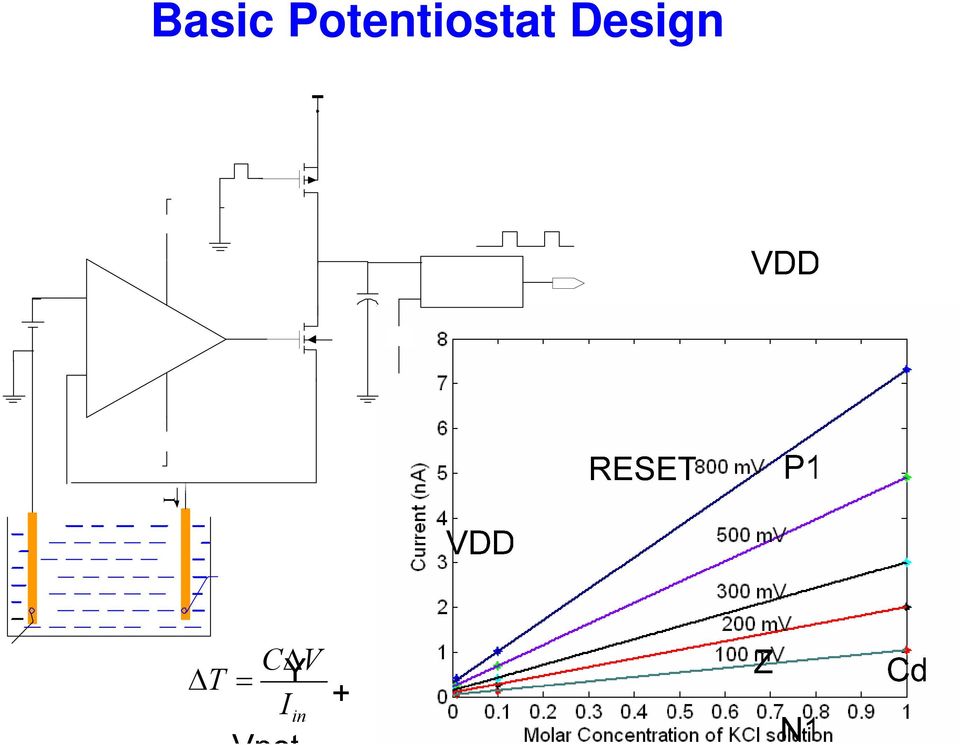
16 Chip Results Analytic vs. Measured Results Measured Specifications: Offset: 5mV Detection limit: 1pA Dynamic range: 116dB Area: 0.025mm 2 Power: 130uW Sensitivity:100fA

17 Case 2: Positive AC Signals x(t) time Signal x(t) is bandlimited to Ω s

18 Standard Nyquist Rate Sampling x(t) T < π Ω s 0 T 2T 3T 4T 5T 6T 7T 8T 9T time Amplitude sampling: record amplitude at predefined time intervals.

19 Standard Nyquist Rate Sampling x(t) T < π Ω s time How to perfectly reconstruct the signal from the samples?

20 Standard Nyquist Rate Sampling x(t) T < π Ω s time The signal is perfectly reconstructed by ideal low-pass filtering the samples using well-known Nyquist theory.

21 Sampling With Integrate-and-fire (IF) Neuron Model x(t) time Signal x(t) is bandlimited to Ω s
22 Sampling With Integrate-and-fire (IF) Neuron Model x(t) Encoding equation t time t i 1 + x( t) dt = t i θ Define the integral: f ( t) = t t 0 x( τ ) dτ
23 Sampling With Integrate-and-fire (IF) Neuron Model f (t) 11θ 10θ 9θ 8θ 7θ 6θ 5θ 4θ 3θ 2θ θ t0 1 2 Define the integral: ( t) The sample time t i meet: f 9 = 10 t t 0 11 time x( τ ) dτ f ( ti ) = iθ Encoding equation t i 1 + x( t) dt = t i θ
24 Sampling With Integrate-and-fire (IF) Neuron Model f (t) 11θ 10θ 9θ 8θ 7θ 6θ 5θ 4θ 3θ 2θ θ Encoding equation t i 1 + x( t) dt = t i θ t time Time sampling: record time at predefined amplitude intervals.
25 Sampling With Integrate-and-fire (IF) Neuron Model Spike T max < π Ω s Encoding equation 1 + x( t) dt = t t i i θ T max time Can low-pass filtering achieve perfect reconstruction? No. Signal band is corrupted by cross-modulated components (Bayly 68).
26 Signal Reconstruction Any bandlimited signal can be expressed as a lowpass filtered version of an appropriately weighted sum of delayed impulse functions. (Derived from Duffin et al. 1952, Feichtinger et al. 1994, Lazar et al.) Signal Impulse train Lowpass Filter Amplitude Time Weight Δt max < π Ω s Time = = xt () ht ()* wδ ( t s) wht ( s) * Ω s Mag j j j j j j Where w j is computed by solving a linear system 1 Ωs Freq
27 Simulation Results (Matlab) X(t) is a Gaussian random noise signal bandlimited to 1.5kHz Maximum ISI = 0.14ms < T SNR = 103dB SNR is limited by the finite number of spikes and finite computational precision
28 Temporal Quantization 110 SNR (db) Clock Period (S) Shows the effect of temporal quantization on SNR. Temporal quantization happens when the spike train is synchronized to a fast clock on a DSP. The plot also gives an idea of how much timing jitter can be allowed in the electronics and in the transmission
29 Frequency Aliasing Shows the effect of frequency aliasing on SNR. SNR (db) Aliasing Freq (Hz) Standard Nyquist Rate Sampling Can we reconstruct the signal from a neuron chip? For IF neuron, the detrimental effect of high frequency aliasing is reduced because of the integration. For standard Nyquist rate sampling, higher frequencies are simply mapped to lower frequencies preserving its power.
30 Integrate-and-fire Neuron Chip Fabricated in AMI C5 0.5u CMOS process V/I converter and IF neuron on the chip
31 Integrate-and-fire Neuron Circuit Implementation Modified Mead Neuron
32 Chip Test Results SNR v.s. Signal freq. 80 SNR (db) Average firing rate is about 100kHz. SNR is above 63dB (Using IEEE std 1241) Power is (66uA)(5V) = 330uW. Have now reached < 50uW (still unoptimized) 0 0 5k 10k 15k 20k 25k 30k Signal Freq. (Hz)
33 Extends to Other Neuron Models Works with refractory period (to limit peak spiking rate) Leaky IF neuron models: Spice simulation of CMOS LIF neurons shows reconstruction SNR > 80dB Neuron with adaptation:
34 Applications 1. ADC replacement 2. Neural amplifier Applications in remote sensing, implanted devices and power-limited systems. Simpler analog circuitry on the remote sensor is traded off for more complex digital reconstruction on the bay station. Simple and low power Robust to transmission noise
35 Bio-amplifier with Pulse Output Input signal: Signal amplitudes: uV Frequency range: 100Hz-6kHz Local Field Potential < 1Hz DC offset of 1-2V Must be low-noise, lowpower and compact
36 Measured Spike Data Input 20uV sinusoid Signal amplified by 100 Spikes are output and reconstructed
37 Measured Performance Midband gain: db Low freq cutoff: ~300mHz High freq cutoff: 5.4kHz Input referred noise: 9.56uVrms Power consumption: 300uW CMRR: >-59.2 db PSRR: ~45 db Dynamic Range: 52.7dB Output DC offset: ~100mV Die area: 0.088mm^2/channel Amplitude (mv) Time (second) Measured in vivo recording (voltage output)
38 Case 3: Signed AC Signals Vth+ + τ P + (t) Vin Gm C Vth- + τ P-(t) Vmid OR P + (t) P-(t) Biphasic pulse coding
39 Measured Chip Data 1 (a) Voltage (mv) Voltage (mv) x 10-3 (b) x 10-3 (c) Time (s) x 10-3 AMI 0.5um CMOS process 100 uw power consumption
40 Sub-Nyquist Rate Sampling (Simulation) Original Fs = 25 khz 18 kspikes/sec 9 kspikes/sec 6 kspikes/sec
41 Conclusions Introduced integrate-and-fire (IF) signal coding IF coding improves sensor performance IF is an alternative to traditional Nyquist sampling and can achieve perfect reconstruction IF is a power- and bandwidth-efficient strategy (outperforms rate codes) We can process these spikes within a mathematical framework (see Jose Principe s talk) Questions?
Sampling and Interpolation. Yao Wang Polytechnic University, Brooklyn, NY11201
 Sampling and Interpolation Yao Wang Polytechnic University, Brooklyn, NY1121 http://eeweb.poly.edu/~yao Outline Basics of sampling and quantization A/D and D/A converters Sampling Nyquist sampling theorem
Department of Electrical and Computer Engineering Ben-Gurion University of the Negev. LAB 1 - Introduction to USRP
 Department of Electrical and Computer Engineering Ben-Gurion University of the Negev LAB 1 - Introduction to USRP - 1-1 Introduction In this lab you will use software reconfigurable RF hardware from National
Sampling Theorem Notes. Recall: That a time sampled signal is like taking a snap shot or picture of signal periodically.
 Sampling Theorem We will show that a band limited signal can be reconstructed exactly from its discrete time samples. Recall: That a time sampled signal is like taking a snap shot or picture of signal
Example/ an analog signal f ( t) ) is sample by f s = 5000 Hz draw the sampling signal spectrum. Calculate min. sampling frequency.
 ) is sample by f s = 5000 Hz draw the sampling signal spectrum. Calculate min. sampling frequency.") 1 2 3 4 Example/ an analog signal f ( t) = 1+ cos(4000πt ) is sample by f s = 5000 Hz draw the sampling signal spectrum. Calculate min. sampling frequency. Sol/ H(f) -7KHz -5KHz -3KHz -2KHz 0 2KHz 3KHz
1 2 3 4 Example/ an analog signal f ( t) = 1+ cos(4000πt ) is sample by f s = 5000 Hz draw the sampling signal spectrum. Calculate min. sampling frequency. Sol/ H(f) -7KHz -5KHz -3KHz -2KHz 0 2KHz 3KHz
Title : Analog Circuit for Sound Localization Applications
 Title : Analog Circuit for Sound Localization Applications Author s Name : Saurabh Kumar Tiwary Brett Diamond Andrea Okerholm Contact Author : Saurabh Kumar Tiwary A-51 Amberson Plaza 5030 Center Avenue
The Effective Number of Bits (ENOB) of my R&S Digital Oscilloscope Technical Paper
 of my R&S Digital Oscilloscope Technical Paper") The Effective Number of Bits (ENOB) of my R&S Digital Oscilloscope Technical Paper Products: R&S RTO1012 R&S RTO1014 R&S RTO1022 R&S RTO1024 This technical paper provides an introduction to the signal
The Effective Number of Bits (ENOB) of my R&S Digital Oscilloscope Technical Paper Products: R&S RTO1012 R&S RTO1014 R&S RTO1022 R&S RTO1024 This technical paper provides an introduction to the signal
Digital Transmission of Analog Data: PCM and Delta Modulation
 Digital Transmission of Analog Data: PCM and Delta Modulation Required reading: Garcia 3.3.2 and 3.3.3 CSE 323, Fall 200 Instructor: N. Vlajic Digital Transmission of Analog Data 2 Digitization process
PIN CONFIGURATION FEATURES ORDERING INFORMATION ABSOLUTE MAXIMUM RATINGS. D, F, N Packages
 DESCRIPTION The µa71 is a high performance operational amplifier with high open-loop gain, internal compensation, high common mode range and exceptional temperature stability. The µa71 is short-circuit-protected
Lock - in Amplifier and Applications
 Lock - in Amplifier and Applications What is a Lock in Amplifier? In a nut shell, what a lock-in amplifier does is measure the amplitude V o of a sinusoidal voltage, V in (t) = V o cos(ω o t) where ω o
Computer Networks and Internets, 5e Chapter 6 Information Sources and Signals. Introduction
 Computer Networks and Internets, 5e Chapter 6 Information Sources and Signals Modified from the lecture slides of Lami Kaya ([email protected]) for use CECS 474, Fall 2008. 2009 Pearson Education Inc., Upper
PCM Encoding and Decoding:
 PCM Encoding and Decoding: Aim: Introduction to PCM encoding and decoding. Introduction: PCM Encoding: The input to the PCM ENCODER module is an analog message. This must be constrained to a defined bandwidth
MATRIX TECHNICAL NOTES
 200 WOOD AVENUE, MIDDLESEX, NJ 08846 PHONE (732) 469-9510 FAX (732) 469-0418 MATRIX TECHNICAL NOTES MTN-107 TEST SETUP FOR THE MEASUREMENT OF X-MOD, CTB, AND CSO USING A MEAN SQUARE CIRCUIT AS A DETECTOR
by Anurag Pulincherry A THESIS submitted to Oregon State University in partial fulfillment of the requirements for the degree of Master of Science
 A Continuous Time Frequency Translating Delta Sigma Modulator by Anurag Pulincherry A THESIS submitted to Oregon State University in partial fulfillment of the requirements for the degree of Master of
US-Key New generation of High performances Ultrasonic device
 US-Key New generation of High performances Ultrasonic device US-Key connected to a laptop computer US-Key Ultrasound device single channel Features USB2 High Speed connection Ultralow noise preamplifier
HA-5104/883. Low Noise, High Performance, Quad Operational Amplifier. Features. Description. Applications. Ordering Information. Pinout.
 HA5104/883 April 2002 Features This Circuit is Processed in Accordance to MILSTD 883 and is Fully Conformant Under the Provisions of Paragraph 1.2.1. Low Input Noise Voltage Density at 1kHz. 6nV/ Hz (Max)
Non-Data Aided Carrier Offset Compensation for SDR Implementation
 Non-Data Aided Carrier Offset Compensation for SDR Implementation Anders Riis Jensen 1, Niels Terp Kjeldgaard Jørgensen 1 Kim Laugesen 1, Yannick Le Moullec 1,2 1 Department of Electronic Systems, 2 Center
Implementation of Digital Signal Processing: Some Background on GFSK Modulation
 Implementation of Digital Signal Processing: Some Background on GFSK Modulation Sabih H. Gerez University of Twente, Department of Electrical Engineering [email protected] Version 4 (February 7, 2013)
6.025J Medical Device Design Lecture 3: Analog-to-Digital Conversion Prof. Joel L. Dawson
 Let s go back briefly to lecture 1, and look at where ADC s and DAC s fit into our overall picture. I m going in a little extra detail now since this is our eighth lecture on electronics and we are more
Programmable Single-/Dual-/Triple- Tone Gong SAE 800
 Programmable Single-/Dual-/Triple- Tone Gong Preliminary Data SAE 800 Bipolar IC Features Supply voltage range 2.8 V to 18 V Few external components (no electrolytic capacitor) 1 tone, 2 tones, 3 tones
Analog Representations of Sound
 Analog Representations of Sound Magnified phonograph grooves, viewed from above: The shape of the grooves encodes the continuously varying audio signal. Analog to Digital Recording Chain ADC Microphone
Digital Modulation. David Tipper. Department of Information Science and Telecommunications University of Pittsburgh. Typical Communication System
 Digital Modulation David Tipper Associate Professor Department of Information Science and Telecommunications University of Pittsburgh http://www.tele.pitt.edu/tipper.html Typical Communication System Source
Frequency Response of Filters
 School of Engineering Department of Electrical and Computer Engineering 332:224 Principles of Electrical Engineering II Laboratory Experiment 2 Frequency Response of Filters 1 Introduction Objectives To
US-SPI New generation of High performances Ultrasonic device
 US-SPI New generation of High performances Ultrasonic device Lecoeur Electronique - 19, Rue de Courtenay - 45220 CHUELLES - Tel. : +33 ( 0)2 38 94 28 30 - Fax : +33 (0)2 38 94 29 67 US-SPI Ultrasound device
Op Amp Circuit Collection
 Op Amp Circuit Collection Note: National Semiconductor recommends replacing 2N2920 and 2N3728 matched pairs with LM394 in all application circuits. Section 1 Basic Circuits Inverting Amplifier Difference
Introduction to Digital Audio
 Introduction to Digital Audio Before the development of high-speed, low-cost digital computers and analog-to-digital conversion circuits, all recording and manipulation of sound was done using analog techniques.
Voice---is analog in character and moves in the form of waves. 3-important wave-characteristics:
 Voice Transmission --Basic Concepts-- Voice---is analog in character and moves in the form of waves. 3-important wave-characteristics: Amplitude Frequency Phase Voice Digitization in the POTS Traditional
Digital to Analog and Analog to Digital Conversion
 Real world (lab) is Computer (binary) is digital Digital to Analog and Analog to Digital Conversion V t V t D/A or DAC and A/D or ADC D/A Conversion Computer DAC A/D Conversion Computer DAC Digital to
Analog and Digital Signals, Time and Frequency Representation of Signals
 1 Analog and Digital Signals, Time and Frequency Representation of Signals Required reading: Garcia 3.1, 3.2 CSE 3213, Fall 2010 Instructor: N. Vlajic 2 Data vs. Signal Analog vs. Digital Analog Signals
b 1 is the most significant bit (MSB) The MSB is the bit that has the most (largest) influence on the analog output
 The MSB is the bit that has the most (largest) influence on the analog output") CMOS Analog IC Design - Chapter 10 Page 10.0-5 BLOCK DIAGRAM OF A DIGITAL-ANALOG CONVERTER b 1 is the most significant bit (MSB) The MSB is the bit that has the most (largest) influence on the analog output
CMOS Analog IC Design - Chapter 10 Page 10.0-5 BLOCK DIAGRAM OF A DIGITAL-ANALOG CONVERTER b 1 is the most significant bit (MSB) The MSB is the bit that has the most (largest) influence on the analog output
Fundamentals of Power Electronics. Robert W. Erickson University of Colorado, Boulder
 Robert W. Erickson University of Colorado, Boulder 1 1.1. Introduction to power processing 1.2. Some applications of power electronics 1.3. Elements of power electronics Summary of the course 2 1.1 Introduction
Lab 5 Getting started with analog-digital conversion
 Lab 5 Getting started with analog-digital conversion Achievements in this experiment Practical knowledge of coding of an analog signal into a train of digital codewords in binary format using pulse code
RF Measurements Using a Modular Digitizer
 RF Measurements Using a Modular Digitizer Modern modular digitizers, like the Spectrum M4i series PCIe digitizers, offer greater bandwidth and higher resolution at any given bandwidth than ever before.
A 10,000 Frames/s 0.18 µm CMOS Digital Pixel Sensor with Pixel-Level Memory
 Presented at the 2001 International Solid State Circuits Conference February 5, 2001 A 10,000 Frames/s 0.1 µm CMOS Digital Pixel Sensor with Pixel-Level Memory Stuart Kleinfelder, SukHwan Lim, Xinqiao
TCOM 370 NOTES 99-4 BANDWIDTH, FREQUENCY RESPONSE, AND CAPACITY OF COMMUNICATION LINKS
 TCOM 370 NOTES 99-4 BANDWIDTH, FREQUENCY RESPONSE, AND CAPACITY OF COMMUNICATION LINKS 1. Bandwidth: The bandwidth of a communication link, or in general any system, was loosely defined as the width of
Controller Design in Frequency Domain
 ECSE 4440 Control System Engineering Fall 2001 Project 3 Controller Design in Frequency Domain TA 1. Abstract 2. Introduction 3. Controller design in Frequency domain 4. Experiment 5. Colclusion 1. Abstract
Fully Differential CMOS Amplifier
 ECE 511 Analog Electronics Term Project Fully Differential CMOS Amplifier Saket Vora 6 December 2006 Dr. Kevin Gard NC State University 1 Introduction In this project, a fully differential CMOS operational
FREQUENCY RESPONSE ANALYZERS
 FREQUENCY RESPONSE ANALYZERS Dynamic Response Analyzers Servo analyzers When you need to stabilize feedback loops to measure hardware characteristics to measure system response BAFCO, INC. 717 Mearns Road
USB 3.0 CDR Model White Paper Revision 0.5
 USB 3.0 CDR Model White Paper Revision 0.5 January 15, 2009 INTELLECTUAL PROPERTY DISCLAIMER THIS WHITE PAPER IS PROVIDED TO YOU AS IS WITH NO WARRANTIES WHATSOEVER, INCLUDING ANY WARRANTY OF MERCHANTABILITY,
CHAPTER 6 Frequency Response, Bode Plots, and Resonance
 ELECTRICAL CHAPTER 6 Frequency Response, Bode Plots, and Resonance 1. State the fundamental concepts of Fourier analysis. 2. Determine the output of a filter for a given input consisting of sinusoidal
Understand the effects of clock jitter and phase noise on sampled systems A s higher resolution data converters that can
 designfeature By Brad Brannon, Analog Devices Inc MUCH OF YOUR SYSTEM S PERFORMANCE DEPENDS ON JITTER SPECIFICATIONS, SO CAREFUL ASSESSMENT IS CRITICAL. Understand the effects of clock jitter and phase
MODULATION Systems (part 1)
") Technologies and Services on Digital Broadcasting (8) MODULATION Systems (part ) "Technologies and Services of Digital Broadcasting" (in Japanese, ISBN4-339-62-2) is published by CORONA publishing co.,
Technologies and Services on Digital Broadcasting (8) MODULATION Systems (part ) "Technologies and Services of Digital Broadcasting" (in Japanese, ISBN4-339-62-2) is published by CORONA publishing co.,
Improving A D Converter Performance Using Dither
 Improving A D Converter Performance Using Dither 1 0 INTRODUCTION Many analog-to-digital converter applications require low distortion for a very wide dynamic range of signals Unfortunately the distortion
The front end of the receiver performs the frequency translation, channel selection and amplification of the signal.
 Many receivers must be capable of handling a very wide range of signal powers at the input while still producing the correct output. This must be done in the presence of noise and interference which occasionally
AN-756 APPLICATION NOTE One Technology Way P.O. Box 9106 Norwood, MA 02062-9106 Tel: 781/329-4700 Fax: 781/326-8703 www.analog.com
 APPLICATION NOTE One Technology Way P.O. Box 9106 Norwood, MA 02062-9106 Tel: 781/329-4700 Fax: 781/326-8703 www.analog.com Sampled Systems and the Effects of Clock Phase Noise and Jitter by Brad Brannon
QUICK START GUIDE FOR DEMONSTRATION CIRCUIT 956 24-BIT DIFFERENTIAL ADC WITH I2C LTC2485 DESCRIPTION
 LTC2485 DESCRIPTION Demonstration circuit 956 features the LTC2485, a 24-Bit high performance Σ analog-to-digital converter (ADC). The LTC2485 features 2ppm linearity, 0.5µV offset, and 600nV RMS noise.
Analog signals are those which are naturally occurring. Any analog signal can be converted to a digital signal.
 3.3 Analog to Digital Conversion (ADC) Analog signals are those which are naturally occurring. Any analog signal can be converted to a digital signal. 1 3.3 Analog to Digital Conversion (ADC) WCB/McGraw-Hill
DIGITAL-TO-ANALOGUE AND ANALOGUE-TO-DIGITAL CONVERSION
 DIGITAL-TO-ANALOGUE AND ANALOGUE-TO-DIGITAL CONVERSION Introduction The outputs from sensors and communications receivers are analogue signals that have continuously varying amplitudes. In many systems
Chapter 6 PLL and Clock Generator
 Chapter 6 PLL and Clock Generator The DSP56300 core features a Phase Locked Loop (PLL) clock generator in its central processing module. The PLL allows the processor to operate at a high internal clock
Taking the Mystery out of the Infamous Formula, "SNR = 6.02N + 1.76dB," and Why You Should Care. by Walt Kester
 ITRODUCTIO Taking the Mystery out of the Infamous Formula, "SR = 6.0 + 1.76dB," and Why You Should Care by Walt Kester MT-001 TUTORIAL You don't have to deal with ADCs or DACs for long before running across
Analog/Digital Conversion. Analog Signals. Digital Signals. Analog vs. Digital. Interfacing a microprocessor-based system to the real world.
 Analog/Digital Conversion Analog Signals Interacing a microprocessor-based system to the real world. continuous range x(t) Analog and digital signals he bridge: Sampling heorem Conversion concepts Conversion
ANALYZER BASICS WHAT IS AN FFT SPECTRUM ANALYZER? 2-1
 WHAT IS AN FFT SPECTRUM ANALYZER? ANALYZER BASICS The SR760 FFT Spectrum Analyzer takes a time varying input signal, like you would see on an oscilloscope trace, and computes its frequency spectrum. Fourier's
NRZ Bandwidth - HF Cutoff vs. SNR
 Application Note: HFAN-09.0. Rev.2; 04/08 NRZ Bandwidth - HF Cutoff vs. SNR Functional Diagrams Pin Configurations appear at end of data sheet. Functional Diagrams continued at end of data sheet. UCSP
12-Bit, 4-Channel Parallel Output Sampling ANALOG-TO-DIGITAL CONVERTER
 For most current data sheet and other product information, visit www.burr-brown.com 12-Bit, 4-Channel Parallel Output Sampling ANALOG-TO-DIGITAL CONVERTER FEATURES SINGLE SUPPLY: 2.7V to 5V 4-CHANNEL INPUT
NTE2053 Integrated Circuit 8 Bit MPU Compatible A/D Converter
 NTE2053 Integrated Circuit 8 Bit MPU Compatible A/D Converter Description: The NTE2053 is a CMOS 8 bit successive approximation Analog to Digital converter in a 20 Lead DIP type package which uses a differential
Timing Errors and Jitter
 Timing Errors and Jitter Background Mike Story In a sampled (digital) system, samples have to be accurate in level and time. The digital system uses the two bits of information the signal was this big
Application Report. 1 Introduction. 2 Resolution of an A-D Converter. 2.1 Signal-to-Noise Ratio (SNR) Harman Grewal... ABSTRACT
 Harman Grewal... ABSTRACT") Application Report SLAA323 JULY 2006 Oversampling the ADC12 for Higher Resolution Harman Grewal... ABSTRACT This application report describes the theory of oversampling to achieve resolutions greater than
Application Report SLAA323 JULY 2006 Oversampling the ADC12 for Higher Resolution Harman Grewal... ABSTRACT This application report describes the theory of oversampling to achieve resolutions greater than
Analog Signal Conditioning
 Analog Signal Conditioning Analog and Digital Electronics Electronics Digital Electronics Analog Electronics 2 Analog Electronics Analog Electronics Operational Amplifiers Transistors TRIAC 741 LF351 TL084
Single Supply Op Amp Circuits Dr. Lynn Fuller
 ROCHESTER INSTITUTE OF TECHNOLOGY MICROELECTRONIC ENGINEERING Single Supply Op Amp Circuits Dr. Lynn Fuller Webpage: http://people.rit.edu/lffeee 82 Lomb Memorial Drive Rochester, NY 146235604 Tel (585)
Step Response of RC Circuits
 Step Response of RC Circuits 1. OBJECTIVES...2 2. REFERENCE...2 3. CIRCUITS...2 4. COMPONENTS AND SPECIFICATIONS...3 QUANTITY...3 DESCRIPTION...3 COMMENTS...3 5. DISCUSSION...3 5.1 SOURCE RESISTANCE...3
Conversion Between Analog and Digital Signals
 ELET 3156 DL - Laboratory #6 Conversion Between Analog and Digital Signals There is no pre-lab work required for this experiment. However, be sure to read through the assignment completely prior to starting
AVR127: Understanding ADC Parameters. Introduction. Features. Atmel 8-bit and 32-bit Microcontrollers APPLICATION NOTE
 Atmel 8-bit and 32-bit Microcontrollers AVR127: Understanding ADC Parameters APPLICATION NOTE Introduction This application note explains the basic concepts of analog-to-digital converter (ADC) and the
MPC 4. Machinery Protection Card Type MPC 4 FEATURES. Continuous on-line Machinery Protection Card
 Machinery Protection Card Type FEATURES Continuous on-line Machinery Protection Card Real-time measurement and monitoring using state-of-the-art DSP techniques Fully VME-compatible slave interface Fully
24-Bit ANALOG-TO-DIGITAL CONVERTER
 ADS1211 ADS1211 ADS1211 ADS1210 ADS1210 ADS1210 ADS1211 JANUARY 1996 REVISED SEPTEMBER 2005 24-Bit ANALOG-TO-DIGITAL CONVERTER FEATURES DELTA-SIGMA A/D CONVERTER 23 BITS EFFECTIVE RESOLUTION AT 10Hz AND
The D.C Power Supply
 The D.C Power Supply Voltage Step Down Electrical Isolation Converts Bipolar signal to Unipolar Half or Full wave Smoothes the voltage variation Still has some ripples Reduce ripples Stabilize the output
Introduction to Receivers
 Introduction to Receivers Purpose: translate RF signals to baseband Shift frequency Amplify Filter Demodulate Why is this a challenge? Interference (selectivity, images and distortion) Large dynamic range
T = 1 f. Phase. Measure of relative position in time within a single period of a signal For a periodic signal f(t), phase is fractional part t p
, phase is fractional part t p") Data Transmission Concepts and terminology Transmission terminology Transmission from transmitter to receiver goes over some transmission medium using electromagnetic waves Guided media. Waves are guided
Data Transmission Concepts and terminology Transmission terminology Transmission from transmitter to receiver goes over some transmission medium using electromagnetic waves Guided media. Waves are guided
AMPLIFIED HIGH SPEED FIBER PHOTODETECTOR USER S GUIDE
 AMPLIFIED HIGH SPEED FIBER PHOTODETECTOR USER S GUIDE Thank you for purchasing your Amplified High Speed Fiber Photodetector. This user s guide will help answer any questions you may have regarding the
DESCRIPTION FEATURES BLOCK DIAGRAM. PT2260 Remote Control Encoder
 Remote Control Encoder DESCRIPTION PT2260 is a remote control encoder paired with either PT2270 or PT2272 utilizing CMOS Technology. It encodes data and address pins into a serial coded waveform suitable
Class D Audio Amplifier
 Class D Audio Amplifier The design of a live audio Class D audio amplifier with greater than 90% efficiency and less than 1% distortion. A Major Qualifying Project Submitted to the Faculty of the WORCESTER
www.jameco.com 1-800-831-4242
 Distributed by: www.jameco.com 1-800-831-4242 The content and copyrights of the attached material are the property of its owner. LF411 Low Offset, Low Drift JFET Input Operational Amplifier General Description
Design of a TL431-Based Controller for a Flyback Converter
 Design of a TL431-Based Controller for a Flyback Converter Dr. John Schönberger Plexim GmbH Technoparkstrasse 1 8005 Zürich 1 Introduction The TL431 is a reference voltage source that is commonly used
NTE923 & NTE923D Integrated Circuit Precision Voltage Regulator
 NTE923 & NTE923D Integrated Circuit Precision Voltage Regulator Description: The NTE923 and NTE923D are voltage regulators designed primarily for series regulator applications. By themselves, these devices
QAM Demodulation. Performance Conclusion. o o o o o. (Nyquist shaping, Clock & Carrier Recovery, AGC, Adaptive Equaliser) o o. Wireless Communications
 o o. Wireless Communications") 0 QAM Demodulation o o o o o Application area What is QAM? What are QAM Demodulation Functions? General block diagram of QAM demodulator Explanation of the main function (Nyquist shaping, Clock & Carrier
0 QAM Demodulation o o o o o Application area What is QAM? What are QAM Demodulation Functions? General block diagram of QAM demodulator Explanation of the main function (Nyquist shaping, Clock & Carrier
TCOM 370 NOTES 99-6 VOICE DIGITIZATION AND VOICE/DATA INTEGRATION
 TCOM 370 NOTES 99-6 VOICE DIGITIZATION AND VOICE/DATA INTEGRATION (Please read appropriate parts of Section 2.5.2 in book) 1. VOICE DIGITIZATION IN THE PSTN The frequencies contained in telephone-quality
1995 Mixed-Signal Products SLAA013
 Application Report 995 Mixed-Signal Products SLAA03 IMPORTANT NOTICE Texas Instruments and its subsidiaries (TI) reserve the right to make changes to their products or to discontinue any product or service
INTRODUCTION TO COMMUNICATION SYSTEMS AND TRANSMISSION MEDIA
 COMM.ENG INTRODUCTION TO COMMUNICATION SYSTEMS AND TRANSMISSION MEDIA 9/6/2014 LECTURES 1 Objectives To give a background on Communication system components and channels (media) A distinction between analogue
Prepared by: Paul Lee ON Semiconductor http://onsemi.com
 Introduction to Analog Video Prepared by: Paul Lee ON Semiconductor APPLICATION NOTE Introduction Eventually all video signals being broadcasted or transmitted will be digital, but until then analog video
Digital to Analog Converter. Raghu Tumati
 Digital to Analog Converter Raghu Tumati May 11, 2006 Contents 1) Introduction............................... 3 2) DAC types................................... 4 3) DAC Presented.............................
LTC1390 8-Channel Analog Multiplexer with Serial Interface U DESCRIPTIO
 FEATRES -Wire Serial Digital Interface Data Retransmission Allows Series Connection with Serial A/D Converters Single V to ±V Supply Operation Analog Inputs May Extend to Supply Rails Low Charge Injection
S2000 Spectrometer Data Sheet
 Description The Ocean Optics OEM S2000 Spectrometer includes the linear CCD-array optical bench, plus the circuits necessary for spectrometer operation. The result is a compact, flexible system with no
28V, 2A Buck Constant Current Switching Regulator for White LED
 28V, 2A Buck Constant Current Switching Regulator for White LED FP7102 General Description The FP7102 is a PWM control buck converter designed to provide a simple, high efficiency solution for driving
PowerAmp Design. PowerAmp Design PAD135 COMPACT HIGH VOLATGE OP AMP
 PowerAmp Design COMPACT HIGH VOLTAGE OP AMP Rev G KEY FEATURES LOW COST SMALL SIZE 40mm SQUARE HIGH VOLTAGE 200 VOLTS HIGH OUTPUT CURRENT 10A PEAK 40 WATT DISSIPATION CAPABILITY 200V/µS SLEW RATE APPLICATIONS
Design of a Wireless Medical Monitoring System * Chavabathina Lavanya 1 G.Manikumar 2
 Design of a Wireless Medical Monitoring System * Chavabathina Lavanya 1 G.Manikumar 2 1 PG Student (M. Tech), Dept. of ECE, Chirala Engineering College, Chirala., A.P, India. 2 Assistant Professor, Dept.
Selected Filter Circuits Dr. Lynn Fuller
 ROCHESTER INSTITUTE OF TECHNOLOGY MICROELECTRONIC ENGINEERING Selected Filter Circuits Dr. Lynn Fuller Webpage: http://people.rit.edu/lffeee 82 Lomb Memorial Drive Rochester, NY 146235604 Tel (585) 4752035
chapter Introduction to Digital Signal Processing and Digital Filtering 1.1 Introduction 1.2 Historical Perspective
 Introduction to Digital Signal Processing and Digital Filtering chapter 1 Introduction to Digital Signal Processing and Digital Filtering 1.1 Introduction Digital signal processing (DSP) refers to anything
A 1-GSPS CMOS Flash A/D Converter for System-on-Chip Applications
 A -GSPS CMOS Flash A/D Converter for System-on-Chip Applications Jincheol Yoo, Kyusun Choi, and Ali Tangel Department of Computer Science & Department of Computer & Engineering Communications Engineering
Equalization/Compensation of Transmission Media. Channel (copper or fiber)
") Equalization/Compensation of Transmission Media Channel (copper or fiber) 1 Optical Receiver Block Diagram O E TIA LA EQ CDR DMUX -18 dbm 10 µa 10 mv p-p 400 mv p-p 2 Copper Cable Model Copper Cable 4-foot
Equalization/Compensation of Transmission Media Channel (copper or fiber) 1 Optical Receiver Block Diagram O E TIA LA EQ CDR DMUX -18 dbm 10 µa 10 mv p-p 400 mv p-p 2 Copper Cable Model Copper Cable 4-foot
MICROPHONE SPECIFICATIONS EXPLAINED
 Application Note AN-1112 MICROPHONE SPECIFICATIONS EXPLAINED INTRODUCTION A MEMS microphone IC is unique among InvenSense, Inc., products in that its input is an acoustic pressure wave. For this reason,
Introduction to IQ-demodulation of RF-data
 Introduction to IQ-demodulation of RF-data by Johan Kirkhorn, IFBT, NTNU September 15, 1999 Table of Contents 1 INTRODUCTION...3 1.1 Abstract...3 1.2 Definitions/Abbreviations/Nomenclature...3 1.3 Referenced
Wideband Driver Amplifiers
 The driver amplifier is a wideband, 1 khz to 4 GHz amplifier intended for use in broadband microwave and high data rate systems. The is a 3-stage high output power modulator driver amplifier that can provide
Digital Transmission (Line Coding)
") Digital Transmission (Line Coding) Pulse Transmission Source Multiplexer Line Coder Line Coding: Output of the multiplexer (TDM) is coded into electrical pulses or waveforms for the purpose of transmission
Digital Transmission (Line Coding) Pulse Transmission Source Multiplexer Line Coder Line Coding: Output of the multiplexer (TDM) is coded into electrical pulses or waveforms for the purpose of transmission
SIGNAL GENERATORS and OSCILLOSCOPE CALIBRATION
 1 SIGNAL GENERATORS and OSCILLOSCOPE CALIBRATION By Lannes S. Purnell FLUKE CORPORATION 2 This paper shows how standard signal generators can be used as leveled sine wave sources for calibrating oscilloscopes.
Android based Alcohol detection system using Bluetooth technology
 For more Project details visit: http://www.projectsof8051.com/android-based-alcohol-detection-system-usingbluetooth-technology/ Code 1435 Project Title Android based Alcohol detection system using Bluetooth
Data Acquisition Basics Lab
 Data Acquisition Basics Lab Introduction Many systems in the body can be modeled as electrical systems that interact with various organs, such as the heart, the brain, and body muscle. These systems communicate
An All-Digital Phase-Locked Loop with High Resolution for Local On-Chip Clock Synthesis
 An All-Digital Phase-Locked Loop with High Resolution for Local On-Chip Clock Synthesis Oliver Schrape 1, Frank Winkler 2, Steffen Zeidler 1, Markus Petri 1, Eckhard Grass 1, Ulrich Jagdhold 1 International
RF Network Analyzer Basics
 RF Network Analyzer Basics A tutorial, information and overview about the basics of the RF Network Analyzer. What is a Network Analyzer and how to use them, to include the Scalar Network Analyzer (SNA),
Precision, Unity-Gain Differential Amplifier AMP03
 a FEATURES High CMRR: db Typ Low Nonlinearity:.% Max Low Distortion:.% Typ Wide Bandwidth: MHz Typ Fast Slew Rate: 9.5 V/ s Typ Fast Settling (.%): s Typ Low Cost APPLICATIONS Summing Amplifiers Instrumentation