Modeling Physical Interconnects (Part 3)
|
|
|
- Derrick Gallagher
- 8 years ago
- Views:
Transcription
1 Modeling Physical Interconnects (Part 3) Dr. José Ernesto Rayas Sánchez 1 Outline Vias Vias in PCBs Types of vias in PCBs Pad and antipad Nonfunctional pads Modeling vias Calculating circuit element values with formulas Obtaining circuit element values from EM simulations 2

2 Vias They implement the vertical connections (conductive columns to connect traces on different layers) Vias exist at many physical levels: (R. Mellitz, 2003) 3 Vias in PCBs They are formed by drilling a hole (either mechanically or with a laser) Blind via: a via not passing through the complete PCB Through hole via: a via passing through the entire PCB stackup Buried via: a via connecting internal layers Conducting vias are plated with copper Plated through hole (PTH): conductive via passing through the entire PCB stackup 4

3 Types of Vias in PCBs (R. Mellitz, 2003) 5 PCB Stackup Example showing a 6-layer stackup (S. C. Thierauf, High-Speed Circuit Board Signal Integrity, Artech, 2004) 6

4 Vias in the PCB Stackup (S. C. Thierauf, High-Speed Circuit Board Signal Integrity, Artech, 2004) 7 Pad or Land A ring of copper that surrounds a plated via (to ensure electrical contact to traces even if there is some misalignment) (S. C. Thierauf, High-Speed Circuit Board Signal Integrity, Artech, 2004) 8
 (S. C.")
5 Antipad A hole in the power/ground plane to avoid electrical contact (S. C. Thierauf, High-Speed Circuit Board Signal Integrity, Artech, 2004) 9 Vias Connecting to Power/Ground Planes Small copper fingers are used for thermal isolation (S. C. Thierauf, High-Speed Circuit Board Signal Integrity, Artech, 2004) 10

6 Nonfunctional Pads They are used to anchor the via to the laminate They increase unwanted capacitive coupling to ground/power planes Increasing the antipad decreases the coupling (S. C. Thierauf, High-Speed Circuit Board Signal Integrity, Artech, 2004) 11 Modeling Vias If the via is electrically small (if t d(via) > 0.1t t ), it can be modeled with a lumped circuit (R. Mellitz, 2003) 12
 > 0.1t t ), it can be modeled with a lumped circuit (R.")
7 Modeling Vias (cont) If the via is electrically small (if t d(via) > 0.1t t ), it can be modeled with a lumped circuit L barrel L barrel = 5.08h[ln(4h / d) + 1] (nh) C pad C pad C pad 1.41ε rdt 1 = D D 2 1 (pf) D 1 : pad diameter (in) D 2 : antipad diameter (in) T : thickness of PCB (in) ε r : relative permeability of the PCB h: via length (in) d: via diameter (in) (H. Johnson and M. Graham, High-Speed Digital Design, Prentice Hall, 1993) 13 Alternative Formula for the Via Inductance If the via is electrically small (if t d(via) > 0.1t t ), it can be modeled with a lumped circuit L barrel C pad C pad L barrel 2 µ 0 h + r + h = hln 2 π r r r + h h: via length (m) r: via radius (m) (M.E. Goldfarb and R.A. Pucel, 1991) 14
 13 Alternative Formula for the Via Inductance If the via is electrically small (if t d(via) > 0.")
8 Modeling Vias Example (R. Mellitz, 2003) 15 Modeling a Plated Through Hole Via (PTH) (R. Mellitz, 2003) 16
 (R.")
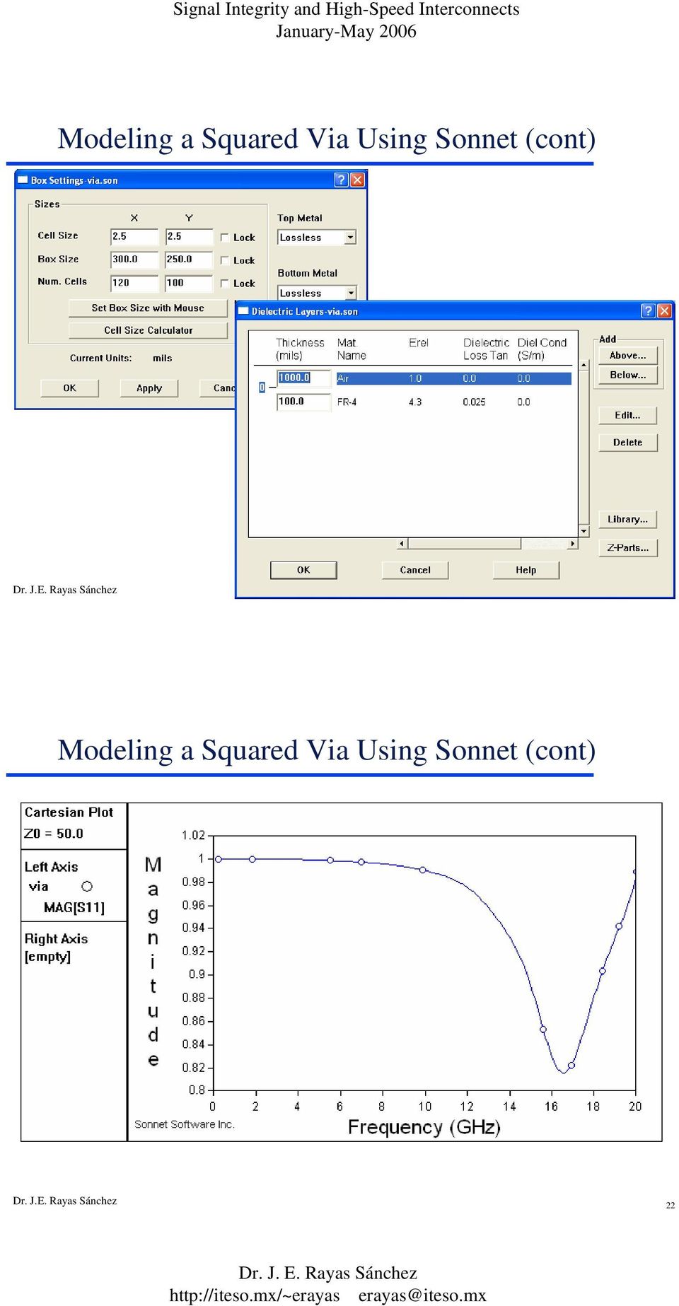
9 Via Modeling though EM Simulation Some electromagnetic simulators have the capability of automatically synthesizing a lumped circuit model using inductors, capacitors, resistors and mutual inductors The equivalent circuit is usually provided in SPICE format This method is intended for any electrically small circuit (small with respect to the wavelength at the highest frequency of excitation) By using this approach, we can develop very accurate models of vias (with arbitrary geometries), without relying on empirical formulas 17 Modeling a Squared Grounded Via Using Sonnet (top layer) 18
, without relying on empirical formulas 17 Modeling a Squared Grounded Via Using Sonnet")
10 (bottom layer, ground) 19 w D D FR4 h w = 50mil D = 80mil H = 100mil ε r = 4.3 loss tan =

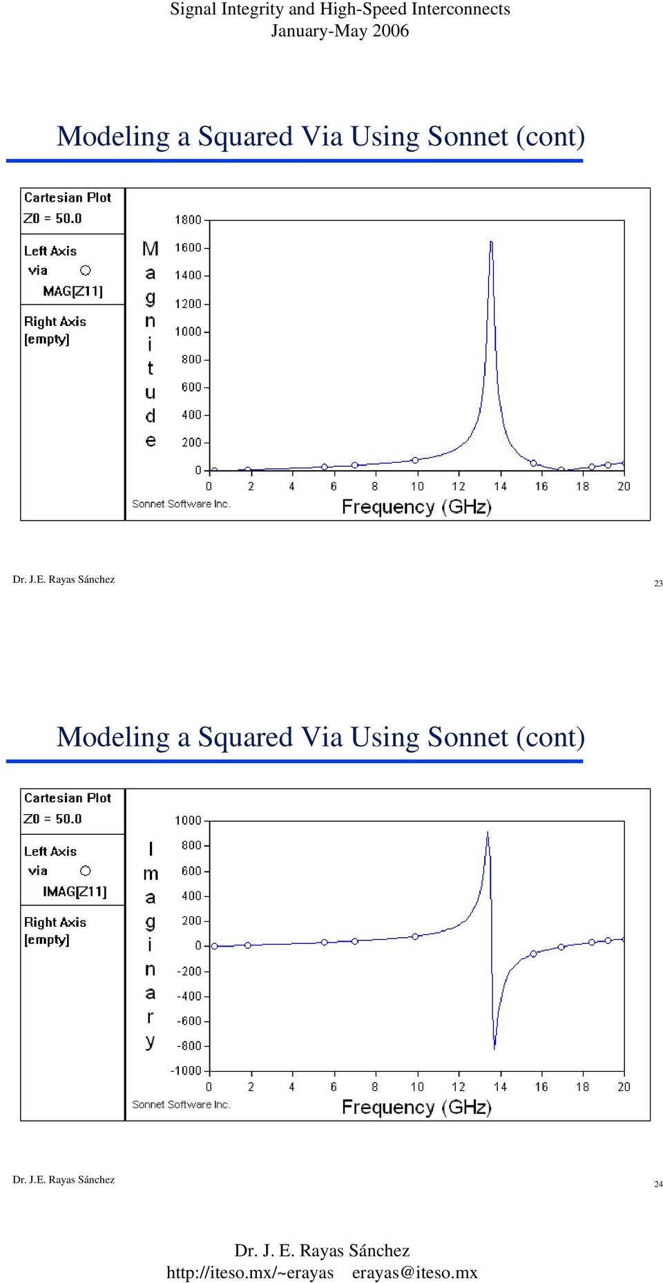
11 21 22
12 23 24
13 200MHz GHz 26
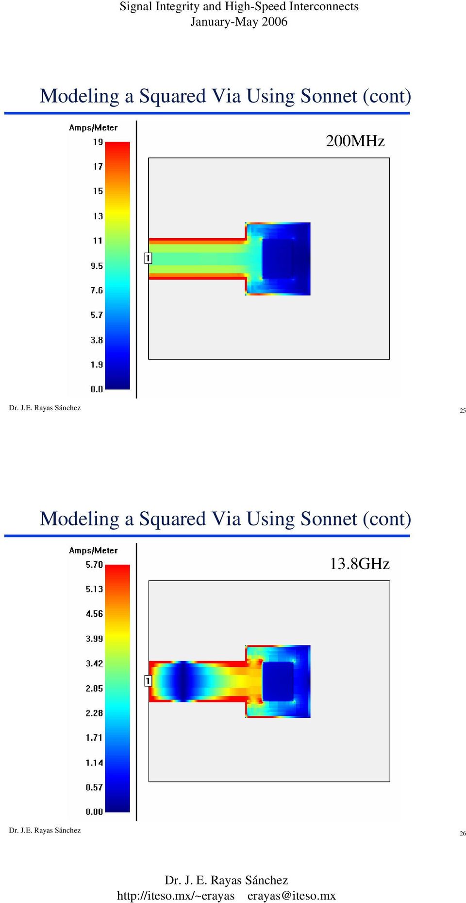
14 20GHz 27 28

15 29 30
16 0.9 Lumped Circuit Model of a Squared Via L C R L (nh) L 808 µh (circuit model above 5GHz is useless) frequency (GHz) Lumped Circuit Model of a Squared Via L 2 C R 1.5 C (pf) 1 C 0.11 pf (circuit model above 5GHz is useless) frequency (GHz) 32
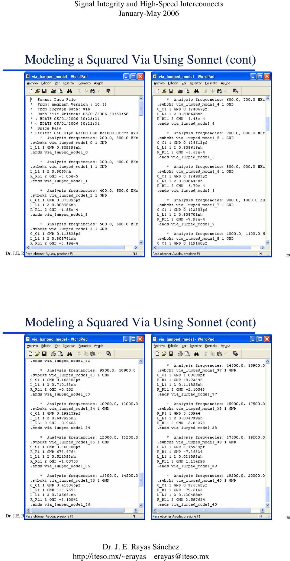
 1 C 0.")
17 4 Lumped Circuit Model of a Squared Via L 3 2 C R 0 Ω R (circuit model above 5GHz is useless) R (ohms) frequency (GHz) 33 Estimating L with Formulas Taking h = 100mil, d = 50mil Using Johnson s formula: L barrel = 5.08h[ln(4h / d) + 1] = nh Using Goldfarb s formula: (r = d/2) L barrel 2 2 µ 0 h + r + h 2 2 = ln = nh 2 h + r r + h π r 34
![Taking h = 100mil, d = 50mil Using Johnson s formula: L barrel = 5.08h[ln(4h / d) + 1] = 1.](/docs-images/44/14397640/images/page_17.jpg "5644 nh Using Goldfarb s formula: (r = d/2) L barrel 2 2 µ 0 h + r + h 2 2 = ln = 0.")
IDT80HSPS1616 PCB Design Application Note - 557
 IDT80HSPS1616 PCB Design Application Note - 557 Introduction This document is intended to assist users to design in IDT80HSPS1616 serial RapidIO switch. IDT80HSPS1616 based on S-RIO 2.0 spec offers 5Gbps
EM Noise Mitigation in Circuit Boards and Cavities
 EM Noise Mitigation in Circuit Boards and Cavities Faculty (UMD): Omar M. Ramahi, Neil Goldsman and John Rodgers Visiting Professors (Finland): Fad Seydou Graduate Students (UMD): Xin Wu, Lin Li, Baharak
PCB Design Conference - East Keynote Address EMC ASPECTS OF FUTURE HIGH SPEED DIGITAL DESIGNS
 OOOO1 PCB Design Conference - East Keynote Address September 12, 2000 EMC ASPECTS OF FUTURE HIGH SPEED DIGITAL DESIGNS By Henry Ott Consultants Livingston, NJ 07039 (973) 992-1793 www.hottconsultants.com
2.996/6.971 Biomedical Devices Design Laboratory Lecture 2: Fundamentals and PCB Layout
 2.996/6.971 Biomedical Devices Design Laboratory Lecture 2: Fundamentals and PCB Layout Instructor: Hong Ma Sept. 12, 2007 Fundamental Elements Resistor (R) Capacitor (C) Inductor (L) Voltage Source Current
Connector Launch Design Guide
 WILD RIVER TECHNOLOGY LLC Connector Launch Design Guide For Vertical Mount RF Connectors James Bell, Director of Engineering 4/23/2014 This guide will information on a typical launch design procedure,
Webinar HDI Microvia Technology Cost Aspects
 Webinar HDI Microvia Technology Cost Aspects www.we-online.com HDI - Cost Aspects Seite 1 1 July, 2014 Agenda - Webinar HDI Microvia Technology Cost Aspects Reasons for the use of HDI technology Printed
Application Note: PCB Design By: Wei-Lung Ho
 Application Note: PCB Design By: Wei-Lung Ho Introduction: A printed circuit board (PCB) electrically connects circuit components by routing conductive traces to conductive pads designed for specific components
ANN Based Modeling of High Speed IC Interconnects. Q.J. Zhang, Carleton University
 ANN Based Modeling of High Speed IC Interconnects Needs for Repeated Simulation Signal integrity optimization Iterative design and re-optimization Monte-Carlo analysis Yield optimization Iterative design
The Critical Length of a Transmission Line
 Page 1 of 9 The Critical Length of a Transmission Line Dr. Eric Bogatin President, Bogatin Enterprises Oct 1, 2004 Abstract A transmission line is always a transmission line. However, if it is physically
How to make a Quick Turn PCB that modern RF parts will actually fit on!
 How to make a Quick Turn PCB that modern RF parts will actually fit on! By: Steve Hageman www.analoghome.com I like to use those low cost, no frills or Bare Bones [1] type of PCB for prototyping as they
RFID Receiver Antenna Project for 13.56 Mhz Band
 RFID Receiver Antenna Project for 13.56 Mhz Band Fatih Eken TE 401 Microwave Course Term Project, Fall 2004 Supervised by Asst. Prof. İbrahim Tekin Telecommunication Program in Faculty of Engineering and
Time and Frequency Domain Analysis for Right Angle Corners on Printed Circuit Board Traces
 Time and Frequency Domain Analysis for Right Angle Corners on Printed Circuit Board Traces Mark I. Montrose Montrose Compliance Services 2353 Mission Glen Dr. Santa Clara, CA 95051-1214 Abstract: For years,
Precision Analog Designs Demand Good PCB Layouts. John Wu
 Precision Analog Designs Demand Good PCB Layouts John Wu Outline Enemies of Precision: Hidden components Noise Crosstalk Analog-to-Analog Digital-to-Analog EMI/RFI Poor Grounds Thermal Instability Leakage
Core Power Delivery Network Analysis of Core and Coreless Substrates in a Multilayer Organic Buildup Package
 Core Power Delivery Network Analysis of Core and Coreless Substrates in a Multilayer Organic Buildup Package Ozgur Misman, Mike DeVita, Nozad Karim, Amkor Technology, AZ, USA 1900 S. Price Rd, Chandler,
Extending Rigid-Flex Printed Circuits to RF Frequencies
 Extending -Flex Printed Circuits to RF Frequencies Robert Larmouth Teledyne Electronic Technologies 110 Lowell Rd., Hudson, NH 03051 (603) 889-6191 Gerald Schaffner Schaffner Consulting 10325 Caminito
Minimizing crosstalk in a high-speed cable-connector assembly.
 Minimizing crosstalk in a high-speed cable-connector assembly. Evans, B.J. Calvo Giraldo, E. Motos Lopez, T. CERN, 1211 Geneva 23, Switzerland John.Evans@cern.ch Eva.Calvo.Giraldo@cern.ch Tomas.Motos-Lopez@cern.ch
Electronic filters design tutorial -2
 In the first part of this tutorial we explored the bandpass filters designed with lumped elements, namely inductors and capacitors. In this second part we will design filters with distributed components
" PCB Layout for Switching Regulators "
 1 " PCB Layout for Switching Regulators " 2 Introduction Linear series pass regulator I L V IN V OUT GAIN REF R L Series pass device drops the necessary voltage to maintain V OUT at it s programmed value
AP24026. Microcontroller. EMC Design Guidelines for Microcontroller Board Layout. Microcontrollers. Application Note, V 3.
 Microcontroller Application Note, V 3.0, April 2005 AP24026 for Microcontroller Board Layout Microcontrollers Never stop thinking. TriCore Revision History: 2005-04 V 3.0 Previous Version: 2001-04 Page
PCB Fabrication Enabling Solutions
 PCB Fabrication Enabling Solutions June 3, 2015 Notice Notification of Proprietary Information: This document contains proprietary information of TTM and its receipt or possession does not convey any rights
IIB. Complete PCB Design Using OrCAD Capture and PCB Editor. Kraig Mitzner. ~»* ' AMSTERDAM BOSTON HEIDELBERG LONDON ^ i H
 Complete PCB Design Using OrCAD Capture and PCB Editor Kraig Mitzner IIB ~»* ' AMSTERDAM BOSTON HEIDELBERG LONDON ^ i H NEW YORK * OXFORD PARIS SAN DIEGO ШШЯтИ' ELSEVIER SAN FRANCISCO SINGAPORE SYDNEY
PCB Board Design. PCB boards. What is a PCB board
 PCB Board Design Babak Kia Adjunct Professor Boston University College of Engineering Email: bkia -at- bu.edu ENG SC757 - Advanced Microprocessor Design PCB boards What is a PCB board Printed Circuit Boards
Return Paths and Power Supply Decoupling
 Return Paths and Power Supply Decoupling Dr. José Ernesto Rayas Sánchez 1 Outline Ideal return paths Microstrip return paths Stripline return paths Modeling metallic reference planes Power supply bypassing
S-PARAMETER MEASUREMENTS OF MEMS SWITCHES
 Radant MEMS employs adaptations of the JMicroTechnology test fixture depicted in Figure 1 to measure MEMS switch s-parameters. RF probeable JMicroTechnology microstrip-to-coplanar waveguide adapter substrates
5. MINIMIZATION OF CONDUCTED EMI. Chapter Five. switch-mode power supply decrease approximately linearly with the increase of the switching
 5. MINIMIZATION OF CONDUCTED EMI Chapter Five MINIMIZATION OF CONDUCTED EMI The sizes of the energy storage elements (transformers, inductors, and capacitors) in a switch-mode power supply decrease approximately
Effective Power/Ground Plane Decoupling for PCB
 Effective Power/Ground Plane Decoupling for PCB Dr. Bruce Archambeault IBM Distinguished Engineer IEEE Fellow IBM Research Triangle Park, NC Barch@us.ibm.com IEEE October 2007 Power Plane Noise Control
CIRCUITS AND SYSTEMS- Assembly and Printed Circuit Board (PCB) Package Mohammad S. Sharawi ASSEMBLY AND PRINTED CIRCUIT BOARD (PCB) PACKAGE
 Package Mohammad S. Sharawi ASSEMBLY AND PRINTED CIRCUIT BOARD (PCB) PACKAGE") ASSEMBLY AND PRINTED CIRCUIT BOARD (PCB) PACKAGE Mohammad S. Sharawi Electrical Engineering Department, King Fahd University of Petroleum and Minerals Dhahran, 31261 Saudi Arabia Keywords: Printed Circuit
ASSEMBLY AND PRINTED CIRCUIT BOARD (PCB) PACKAGE Mohammad S. Sharawi Electrical Engineering Department, King Fahd University of Petroleum and Minerals Dhahran, 31261 Saudi Arabia Keywords: Printed Circuit
Figure 1. Core Voltage Reduction Due to Process Scaling
 AN 574: Printed Circuit Board (PCB) Power Delivery Network (PDN) Design Methodology May 2009 AN-574-1.0 Introduction This application note provides an overview of the various components that make up a
High-Speed Printed Circuit
 The World Leader in High Performance Signal Processing Solutions A Practical Guide to High-Speed Printed Circuit Board Layout John Ardizzoni Analog Devices Dennis Falls Avnet Electronics Marketing Agenda
Rogers 3003, 3006, 3010, 3035, 3203, 3206, 3210
 Stocked Materials: RIGID STANDARD FR4 High Tg 170c Black FR4 Polyclad 370HR (Lead Free) HIGH RELIABILITY Polyimide (Arlon 85N, Isola P96) BT (G200) HIGH FREQUENCY: Park Nelco 4000-13, 4000-13si Getek Gore
Eatman Associates 2014 Rockwall TX 800-388-4036 rev. October 1, 2014. Striplines and Microstrips (PCB Transmission Lines)
") Eatman Associates 2014 Rockwall TX 800-388-4036 rev. October 1, 2014 Striplines and Microstrips (PCB Transmission Lines) Disclaimer: This presentation is merely a compilation of information from public
Eatman Associates 2014 Rockwall TX 800-388-4036 rev. October 1, 2014 Striplines and Microstrips (PCB Transmission Lines) Disclaimer: This presentation is merely a compilation of information from public
Webinar: HDI 2 Perfection in HDI Optimal use of the HDI technology Würth Elektronik Circuit Board Technology
 Webinar: HDI 2 Perfection in HDI Optimal use of the HDI technology Würth Elektronik Circuit Board Technology www.we-online.de Seite 1 04.09.2013 Agenda Overview Webinar HDI 1 Route out a BGA Costs Roadmap
Connectivity in a Wireless World. Cables Connectors 2014. A Special Supplement to
 Connectivity in a Wireless World Cables Connectors 204 A Special Supplement to Signal Launch Methods for RF/Microwave PCBs John Coonrod Rogers Corp., Chandler, AZ COAX CABLE MICROSTRIP TRANSMISSION LINE
Application Note AN:005. FPA Printed Circuit Board Layout Guidelines. Introduction Contents. The Importance of Board Layout
 FPA Printed Circuit Board Layout Guidelines By Paul Yeaman Principal Product Line Engineer V I Chip Strategic Accounts Introduction Contents Page Introduction 1 The Importance of 1 Board Layout Low DC
A SURVEY AND TUTORIAL OF DIELECTRIC MATERIALS USED IN THE MANUFACTURE OF PRINTED CIRCUIT BOARDS.
 A SURVEY AND TUTORIAL OF DIELECTRIC MATERIALS USED IN THE MANUFACTURE OF PRINTED CIRCUIT BOARDS. By Lee W. Ritchey, Speeding Edge, for publication in November 1999 issue of Circuitree magazine. Copyright
Prototyping Printed Circuit Boards
 Prototyping Printed Circuit Boards From concept to prototype to production. (HBRC) PCB Design and Fabrication Agenda Introduction Why PCBs? Stage 1 Understanding the rules Stage 2 Planning the board. Stage
Product Datasheet P1110 915 MHz RF Powerharvester Receiver
 DESCRIPTION The Powercast P1110 Powerharvester receiver is an RF energy harvesting device that converts RF to DC. Housed in a compact SMD package, the P1110 receiver provides RF energy harvesting and power
Managing Connector and Cable Assembly Performance for USB SuperSpeed
 Whitepaper Managing Connector and Cable Assembly Performance for USB SuperSpeed Revision 1.0 February 1, 2013 Abstract USB 3.0 connector and cable assembly performance can have a significant impact on
Product Name Hexa-Band Cellular SMD Antenna GSM / CDMA / DCS / PCS / WCDMA /UMTS /HSDPA / GPRS / EDGE 800 MHz to 2200 MHz
 Anam PA.25a Specification Part No. PA.25a Product Name Anam Hexa-Band Cellular SMD Antenna GSM / CDMA / DCS / PCS / WCDMA /UMTS /HSDPA / GPRS / EDGE 800 MHz to 2200 MHz Feature High Efficiency Multi-Band
Designing with High-Density BGA Packages for Altera Devices
 2014.12.15 Designing with High-Density BGA Packages for Altera Devices AN-114 Subscribe As programmable logic devices (PLDs) increase in density and I/O pins, the demand for small packages and diverse
PCIE 16X CONNECTOR BOARD ROUTING RECOMMENDATIONS TABLE OF CONTENTS
 TABLE OF CONTENTS 1.0 SCOPE 2.0 PC BOARD REQUIREMENTS 2.1 MATERIAL THICKNESS 2.2 TOLERANCE 2.3 HOLE DIMENSIONS 2.4 LAYOUT 3.0 HIGHSPEED ROUTING 3.1 GENERAL ROUTING EXAMPLE 3.2 HIGH-SPEED TRANSMISSION LINE
Dynamic & Proto Circuits Inc. Corporate Presentation
 Dynamic & Proto Circuits Inc. Corporate Presentation 1 DAPC Facility 54,000 Sq.ft./6,000 Sq.M 2 Multilayer Process 3 Solder Mask Options BLUE BLACK RED GREEN DRY FILM CLEAR 4 Investing in Technology New
Switching Regulator Series PCB Layout Techniques of Buck Converter
 Switching Regulator Series PCB ayout Techniques of Buck Converter No.07EBY05 PCB layout design for switching power supply is as important as the circuit design. Appropriate layout can avoid various problems
FABRICATION 2011 SERVICES TECHNOLOGIES CAPABILITIES INDUSTRY
 FABRICATION 2011 SERVICES 24HRS - 5 DAYS ON QUICK TURN PROTOTYPE Dear Customer, We would like to take this opportunity to welcome you and thank you for looking to ASA PCB as your Printed Circuit Manufacturing
Frank Hong Advanced CAE Lab, Telecommunication R&D Center, Telecommunication Business, SAMSUNG ELECTRONICS, Suwon, Republic of Korea
 Slots on Ground Fillings of Multi-layer Printed Circuit Board for Suppressing Indirect Crosstalk between Digital Clock Line and RF Signal Line in Mixed Mode Mobile Systems Jun So Pak School of Electrical
CONCEPT-II. Overview of demo examples
 CONCEPT-II CONCEPT-II is a frequency domain method of moment (MoM) code, under development at the Institute of Electromagnetic Theory at the Technische Universität Hamburg-Harburg (www.tet.tuhh.de). Overview
AN-837 APPLICATION NOTE
 APPLICATION NOTE One Technology Way P.O. Box 916 Norwood, MA 262-916, U.S.A. Tel: 781.329.47 Fax: 781.461.3113 www.analog.com DDS-Based Clock Jitter Performance vs. DAC Reconstruction Filter Performance
LS RS. Figure 1: Assumed inductor model
 Characterizing Inductors at HF and VHF Inductors are a key component in RF circuits. Their performance makes a great difference in the operation of amplifiers, oscillators, and other circuit blocks --
Standex-Meder Electronics. Custom Engineered Solutions for Tomorrow
 Standex-Meder Electronics Custom Engineered Solutions for Tomorrow RF Reed Relays Part II Product Training Copyright 2013 Standex-Meder Electronics. All rights reserved. Introduction Purpose Designing
When designing. Inductors at UHF: EM Simulation Guides Vector Network Analyzer. measurement. EM SIMULATION. There are times when it is
 Inductors at UHF: EM Simulation Guides Vector Network Analyzer Measurements John B. Call Thales Communications Inc., USA When designing There are times when it is circuits for necessary to measure a operation
Consideration of a high-capacity foil cable:
 Consideration of a high-capacity foil cable: Newly discovered ancient knowledge. The old RF-developers already knew the benefits of longplanar lines and have been used (electronic) Eonen (times) thin flat
RF / Microwave PC Board Design and Layout
 RF / Microwave PC Board Design and Layout Rick Hartley L-3 Avionics Systems richard.hartley@l-3com.com 1 Contents 1) Recommended Reading List 2) Basics 3) Line Types and Impedance 4) Integral Components
An Introduction to High-Frequency Circuits and Signal Integrity
 An Introduction to High-Frequency Circuits and Signal Integrity 1 Outline The electromagnetic spectrum Review of market and technology trends Semiconductors industry Computers industry Communication industry
This application note is written for a reader that is familiar with Ethernet hardware design.
 AN18.6 SMSC Ethernet Physical Layer Layout Guidelines 1 Introduction 1.1 Audience 1.2 Overview SMSC Ethernet products are highly-integrated devices designed for 10 or 100 Mbps Ethernet systems. They are
INEMI 2007 Roadmap Organic Substrates. Jack Fisher, Interconnect Technology Analysis, Inc. Celestica-iNEMI Technology Forum May 15, 2007
 INEMI 2007 Roadmap Organic Substrates Jack Fisher, Interconnect Technology Analysis, Inc. Celestica-iNEMI Technology Forum May 15, 2007 Introduction The interconnecting substrates functional role provides
Capacitor Self-Resonance
 Capacitor Self-Resonance By: Dr. Mike Blewett University of Surrey United Kingdom Objective This Experiment will demonstrate some of the limitations of capacitors when used in Radio Frequency circuits.
Guidelines for Designing High-Speed FPGA PCBs
 Guidelines for Designing High-Speed FPGA PCBs February 2004, ver. 1.1 Application Note Introduction Over the past five years, the development of true analog CMOS processes has led to the use of high-speed
PL-277x Series SuperSpeed USB 3.0 SATA Bridge Controllers PCB Layout Guide
 Application Note PL-277x Series SuperSpeed USB 3.0 SATA Bridge Controllers PCB Layout Guide Introduction This document explains how to design a PCB with Prolific PL-277x SuperSpeed USB 3.0 SATA Bridge
An equivalent circuit of a loop antenna.
 3.2.1. Circuit Modeling: Loop Impedance A loop antenna can be represented by a lumped circuit when its dimension is small with respect to a wavelength. In this representation, the circuit parameters (generally
Basic Concepts of Power Distribution Network Design for High-Speed Transmission
 The Open Optics Journal, 2011, 5, (Suppl 1-M8) 51-61 51 Open Access Basic Concepts of Power Distribution Network Design for -Speed Transmission F. Carrió *, V. González and E. Sanchis Department of Electronic
Software for Design NMR Probes Using the Shielded Split Ring and the Shielded Symmetrical Band Resonators
 Software for Design NMR Probes Using the Shielded Split Ring and the Shielded Symmetrical Band Resonators Nasreddine Benahmed University of Tlemcen, Algeria ABSTRACT This article presents a software (NMR
45. The peak value of an alternating current in a 1500-W device is 5.4 A. What is the rms voltage across?
 PHYS Practice Problems hapters 8- hapter 8. 45. The peak value of an alternating current in a 5-W device is 5.4 A. What is the rms voltage across? The power and current can be used to find the peak voltage,
DESIGN GUIDELINES FOR LTCC
 DESIGN GUIDELINES FOR LTCC HERALOCK HL2000 MATERIALS SYSTEM Preliminary Guideline Release 1.0 CONTENTS 1. INTRODUCTION 1.1. GLOSSARY OF TERMS 1.2. LTCC PROCESS FLOW DIAGRAM 1.3. UNITS OF MEASURE 2. PROCESSING
Application Note 58 Crystal Considerations for Dallas Real-Time Clocks
 www.maxim-ic.com Application Note 58 Crystal Considerations for Dallas Real-Time Clocks OVERVIEW This application note describes crystal selection and layout techniques for connecting a 32,768Hz crystal
Symbol Parameters Units Frequency Min. Typ. Max. 850 MHz 14.8 16.3 17.8
 Product Description Sirenza Microdevices SGC-689Z is a high performance SiGe HBT MMIC amplifier utilizing a Darlington configuration with a patented active-bias network. The active bias network provides
Flexible Circuit Simple Design Guide
 Flexible Circuit Simple Design Guide INDEX Flexible Circuit Board Types and Definitions Design Guides and Rules Process Flow Raw Material Single Side Flexible PCB Single Side Flexible PCB (Cover layer
Accelerometer and Gyroscope Design Guidelines
 Application Note Accelerometer and Gyroscope Design Guidelines PURPOSE AND SCOPE This document provides high-level placement and layout guidelines for InvenSense MotionTracking devices. Every sensor has
Simulation and Design Route Development for ADEPT-SiP
 Simulation and Design Route Development for ADEPT-SiP Alaa Abunjaileh, Peng Wong and Ian Hunter The Institute of Microwaves and Photonics School of Electronic and Electrical Engineering The University
3 Embedded Capacitor Material
 3 Embedded Capacitor Material Design and Processing Guidelines for Printed Circuit Board Fabricators Effective date: March 2004 Contents Overview Material Handling Process Compatibility Standard vs. Sequential
ILB, ILBB Ferrite Beads
 ILB, ILBB Ferrite Beads Electro-Magnetic Interference and Electro-Magnetic Compatibility (EMI/EMC) avid B. Fancher Inductive Products ivision INTROUCTION Manufacturers of electrical and electronic equipment
Impedance Matching and Matching Networks. Valentin Todorow, December, 2009
 Impedance Matching and Matching Networks Valentin Todorow, December, 2009 RF for Plasma Processing - Definition of RF What is RF? The IEEE Standard Dictionary of Electrical and Electronics Terms defines
Keeping Current to Stay Competitive in Flex PCB Laser Processing
 White Paper Keeping Current to Stay Competitive in Flex PCB Laser Processing Market Drivers, Trends and Methodologies ESI by Patrick Riechel, PCB Product Manager The push for smaller, cheaper and more
Multi-Flex Circuits Aust.
 Contents: Base Materials Laminate Prepreg Panel Size (Utilization) Multilayer Layup N.C. Drilling Pattern design Impedance control Solder mask type Legend PCB Finishing Gold Plating Profiling Final testing
Technical Support Package
 NASA s Jet Propulsion Laboratory Pasadena, California 91109-8099 Technical Support Package Stripline/Microstrip Transition in Multilayer Circuit Board NASA Tech Briefs NPO-41061 National Aeronautics and
S-Band Low Noise Amplifier Using the ATF-10136. Application Note G004
 S-Band Low Noise Amplifier Using the ATF-10136 Application Note G004 Introduction This application note documents the results of using the ATF-10136 in low noise amplifier applications at S band. The ATF-10136
AN-0971 APPLICATION NOTE
 APPLICATION NOTE One Technology Way P.O. Box 9106 Norwood, MA 02062-9106, U.S.A. Tel: 781.329.4700 Fax: 781.461.3113 www.analog.com Recommendations for Control of Radiated Emissions with isopower Devices
Ultra Reliable Embedded Computing
 A VersaLogic Focus on Reliability White Paper Ultra Reliable Embedded Computing The Clash between IPC Class 3 Requirements and Shrinking Geometries Contents Introduction...1 Case in Point: IPC Class 3
Part 4 PCB LAYOUT RULES FOR SIGNAL INTEGRITY
 Part 4 PCB LAYOUT RULES FOR SIGNAL INTEGRITY The information in this work has been obtained from sources believed to be reliable. The author does not guarantee the accuracy or completeness of any information
Microsystem technology and printed circuit board technology. competition and chance for Europe
 Microsystem technology and printed circuit board technology competition and chance for Europe Prof. Udo Bechtloff, KSG Leiterplatten GmbH 1 Content KSG a continuously growing company PCB based Microsystems
Company Introduction. Welcome to BEST. bestpcbs.com. http://www.bestpcbs
 Company Introduction Welcome to BEST http://www.bestpcbs bestpcbs.com Company Introduction YOUR BEST SOURCE IN ASIA We are dedicated to providing quality, service and value to our customers While maintaining
Chapter 14. Printed Circuit Board
 Chapter 14 Printed Circuit Board A printed circuit board, or PCB, is used to mechanically support and electrically connect electronic components using conductive pathways, or traces, etched from copper
Central Texas Electronics Association PCB Manufacturing Technologies Now and the Future
 Central Texas Electronics Association PCB Manufacturing Technologies Now and the Future Presented by Bryan Fish National Sales Manager SOMACIS / Hallmark Circuits Who am I.. The first 15 years. Sun Circuits,
AN-1109 APPLICATION NOTE
 APPLICATION NOTE One Technology Way P.O. Box 9106 Norwood, MA 02062-9106, U.S.A. Tel: 781.329.4700 Fax: 781.461.3113 www.analog.com Recommendations for Control of Radiated Emissions with icoupler Devices
Effective Power Integrity Floor-Planning and Success Stories in Japan
 Effective Power Integrity Floor-Planning and Success Stories in Japan Giga Hertz Technology Inc, CEO Ryuji Kawamura 1 Agenda 1. Early Stage PI analysis Needs 2. Basic PI theories 3. Floor-planning PI analysis
Analog Devices Welcomes Hittite Microwave Corporation NO CONTENT ON THE ATTACHED DOCUMENT HAS CHANGED
 Analog Devices Welcomes Hittite Microwave Corporation NO CONTENT ON THE ATTACHED DOCUMENT HAS CHANGED www.analog.com www.hittite.com THIS PAGE INTENTIONALLY LEFT BLANK v2.71 HMC42ST8 / 42ST8E AMPLIFIER,.4-2.2
Mitigating Power Bus Noise with Embedded Capacitance in PCB Designs
 Mitigating Power Bus Noise with Embedded Capacitance in PCB Designs Minjia Xu, Todd H. Hubing, Juan Chen*, James L. Drewniak, Thomas P. Van Doren, and Richard E. DuBroff Electromagnetic Compatibility Laboratory
Lead-Free Product Transition: Impact on Printed Circuit Board Design and Material Selection
 Presented in the ECWC 10 Conference at IPC Printed Circuits Expo, SMEMA Council AP EX and Designers Summit 05 Lead-Free Product Transition: Impact on Printed Circuit Board Design and Material Selection
Single Transistor FM Transmitter Design
 Single Transistor FM Transmitter Design In telecommunications, frequency modulation (FM) conveys information over a carrier wave by varying its frequency. FM is commonly used at VHF radio frequencies for
www.pdffactory.com The T-lam System
 The T-lam System T-lam..Where It All Begins.. T-preg The Heart of the T-lam System Three Main Functions Conducts Heat Insulate Electrically Adhesive Bonding Layer The T-lam System T-Preg Thermally Conductive
Flexible Solutions. Hubert Haidinger Director PE/CAM BU Industrial & Automotive 5.June 2013. www.ats.net
 Flexible Solutions Hubert Haidinger Director PE/CAM BU Industrial & Automotive 5.June 2013 www.ats.net Austria Technologie & Systemtechnik Aktiengesellschaft Fabriksgasse13 A-8700 Leoben Tel +43 (0) 3842
Simulation and Design of Printed Circuit Boards Utilizing Novel Embedded Capacitance Material
 Simulation and Design of Printed Circuit Boards Utilizing Novel Embedded Capacitance Material Yu Xuequan, Yan Hang, Zhang Gezi, Wang Haisan Huawei Technologies Co., Ltd Lujiazui Subpark, Pudong Software
CHARACTERIZATION OF A PRINTED CIRCUIT BOARD VIA
 CHARACTERIZATION OF A PRINTED CIRCUIT BOARD VIA by Brock J. LaMeres B.S.E.E., Montana State University, 1998 Technical Report EAS_ECE_2000_09 A thesis submitted to the Graduate Faculty of the University
Signal Integrity: Tips and Tricks
 White Paper: Virtex-II, Virtex-4, Virtex-5, and Spartan-3 FPGAs R WP323 (v1.0) March 28, 2008 Signal Integrity: Tips and Tricks By: Austin Lesea Signal integrity (SI) engineering has become a necessary
Enhanced interconnect medium simplifies test & verification Abstract Introduction Spring Probe Contact Resistance
 Enhanced interconnect medium simplifies test & verification Ila Pal, Ironwood Electronics, Inc. Abstract In high performance embedded systems test application, the requirement for accurate measurement
DEPARTMENT OF DEFENSE TEST METHOD STANDARD METHOD OF INSERTION LOSS MEASUREMENT
 INCH-POUND MIL-STD-220C 14 May 2009 SUPERSEDING MIL-STD-220B 24 January 2000 DEPARTMENT OF DEFENSE TEST METHOD STANDARD METHOD OF INSERTION LOSS MEASUREMENT AMSC N/A FSC EMCS FOREWORD 1. This standard
EMI and t Layout Fundamentals for Switched-Mode Circuits
 v sg (t) (t) DT s V pp = n - 1 2 V pp V g n V T s t EE core insulation primary return secondary return Supplementary notes on EMI and t Layout Fundamentals for Switched-Mode Circuits secondary primary
Since any real component also has loss due to the resistive component, the average power dissipated is 2 2R
 Quality factor, Q Reactive components such as capacitors and inductors are often described with a figure of merit called Q. While it can be defined in many ways, it s most fundamental description is: Q
RF data receiver super-reactive ASK modulation, low cost and low consumption ideal for Microchip HCS KEELOQ decoder/encoder family. 0.
 Receiver AC-RX2/CS RF data receiver super-reactive ASK modulation, low cost and low consumption ideal for Microchip HCS KEELOQ decoder/encoder family. Pin-out 38.1 3 Component Side 1 2 3 7 11 13 14 15
National Laboratory of Antennas and Microwave Technology Xidian University Xi an, Shaanxi 710071, China
 Progress In Electromagnetics Research, PIER 76, 237 242, 2007 A BROADBAND CPW-FED T-SHAPE SLOT ANTENNA J.-J. Jiao, G. Zhao, F.-S. Zhang, H.-W. Yuan, and Y.-C. Jiao National Laboratory of Antennas and Microwave