Simulation and Design Route Development for ADEPT-SiP
|
|
|
- Donald Eric Hancock
- 8 years ago
- Views:
Transcription
1 Simulation and Design Route Development for ADEPT-SiP Alaa Abunjaileh, Peng Wong and Ian Hunter The Institute of Microwaves and Photonics School of Electronic and Electrical Engineering The University of Leeds Malcolm Edwards AWR Ltd. Copyright 2006

2 Outline HDI/ Substrate Architecture Passive Components Modelling Resistors Capacitors Inductors Transmission lines/resonators Work Plan and Developments End Users Demonstrators AWR Production Design Kit

3 ADEPT-SiP Architecture encapsulation ADEPT-SiP module active devices embedded passives HDI substrate motherboard

4 ADEPT-SiP PCB Substrate Architecture The ADEPT-SiP printed circuit board architecture involves: 6-layer board construction with 2 conductor layer core sequential build-up. High Density Interconnect (HDI) layers on either side of this core. R, L, C embedded passives in M1-M3.
 layers on either side of this core.")
5 Design Rules HDI/Microvia Outer Layer Track width>100μm Distance track-track width>125μm Inner Layer Track width>100μm Distance track-track width>100μm Microvia Standard - padφ=300μm Stacked - padφ=300μm End Φ=100μm

6 Design route development Well-defined process architecture Stable process & known capabilities Produce component characterisation boards RFOW measurements S-parameter extraction Model generation Design kit integration Ground Signal Ground Ground Signal Ground Source: IMEC, Intarsia/Dow

7 Design route application design specification schematic capture - hierarchical simulation & optimisation component generation circuit layout re-simulation design tolerance & yield Component & Layout Libraries Models Design Specification Circuit Description Analysis Optimisation design for test, reliability... mask layout verification - DRC, LVS design documentation Design Rules Layout Verification Fabrication

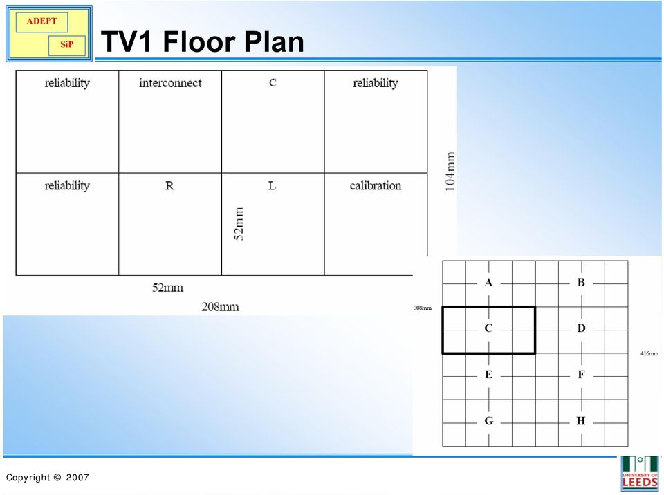
8 Passive Components Simulations Test Vehicle 1 (TV1) Modelling and Simulations Summery: 30 Microstrip transmission lines (including coplanar) 48 Spiral Inductors ( Square and Circular) 56 Capacitors (PTF and Prepreg) 48 Resistors
 56 Capacitors (PTF and")
9 TV1 Floor Plan
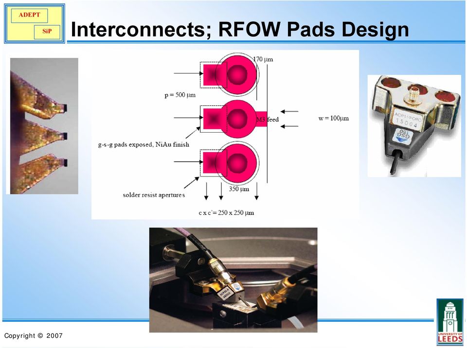
10 Interconnects; RFOW Pads Design
11 Transmission lines Interconnect coupon is divided into four 25x25mm areas, where the line lengths are 5, 10 and 20mm. Zo (Ω) Tx line type Structure Line width (μm) (w-width, s-spacing) 50 Microstrip M1M3 (M1 trace, M3 ground) w50+15=>170 i.w50=>185 ii.w50-15=> Microstrip M2M3 (M2 trace, M3 ground) w50+15=>113 i.w50=>98 50 CPW M2 coplanar w=1880, s= CPW M1 coplanar w=1080, s= CPW M1 coplanar w=100, s=130
 w50+15=>170 i.w50=>185 ii.w50-15=>200 50 Microstrip M2M3 (M2 trace, M3 ground) w50+15=>113 i.")
12 Transmission Lines and Resonators Coplanar Waveguide M1 (Ground Plane), t= 36 μ m Zo = 100Ω l = 5, 10, 20mm, h=60 μ m εr=5.4, tangent loss= Supported Coplanar Waveguide* M2 (Ground Plane), t= 9 μ m Zo = 50 Ω, 100Ω l = 5, 10, 20mm, h=60 μ m εr=5.4, tangent loss=0.035 *S. S. Bedair and I. Wolff, Fast, Accurate and Simple Approximate Analysis Formulas for Calculating the Parameters of Supported Coplanar Waveguides for MMIC s, IEEE Trans. Microwave Theory Tech., Vol.40, No. 1, pp , Jan

13 Polymer Thick Film Resistors 100Ω/square carbon based inks are used. Length(mm) Width (mm) 0.5mm family 1.0mm family 2.0mm family 3.0mm family width width width width Ω 200 Ω 50Ω 100 Ω 300 Ω 150 Ω 600 Ω 300 Ω 25Ω 50Ω 75Ω 150 Ω Ω 33.3 Ω 50Ω 100 Ω 1000 Ω 500Ω 250Ω Ω

14 Capacitors Two classes of capacitors: Polymer Thick Film Capacitors Prepreg Capacitors

15 PTF Capacitors Thickness 20um Dielectric constant = 40 Capacitance 16pF/mm 2

16 Prepreg Capacitors Thickness 50um Dielectric constant = 4 Capacitance 1pF/mm 2

17 Capacitance (pf) Prepreg Capacitor M1M2_THRU_M3_KEEPOUTS-Cal M1M2_THRU_M3_KEEPOUTS-Sim M1M2_THRU_M3_GROUNDED-Cal M1M2_THRU_M3_GROUNDED-Sim M1M2_COMMON_ELECTRODE_THRU_M3_KEEPOUTS-Sim Dimensions (Squared mm)

18 ResonantFreq (GHz) Prepreg Capacitor M1M2_THRU_M3_KEEPOUTS-Res M1M2_COMMON_ELECTRODE_THRU_M3_KEEPOUTS-Res M1M2_THRU_M3_GROUNDED-Res Dimensions (Squared mm)

19 30 25 Prepreg Capacitor M2M3_GROUNDED-Cal M2M3_GROUNDED-Sim M2M3_GROUNDED-Res Capacitance (pf) Resonant Freq (GHz) Dimensions (mm2) 0
 0 1 1.5 2 2.5 3 3.")
20 Inductors TV1 include Square and Circular Spiral inductor classes. The inductor spirals are defined on Conductive Layer 1 (M1) and the underpass on Conductive Layer 2 (M2). The Gnd plane under the inductor is removed.
 and the underpass on Conductive Layer 2 (M2).")
21 Inductors 120 Inductors; Circular Spirals with Gnd keep outs of 125, 250 and 500um Inductance nh L125 L250 L500 L_Q_250 L_Q_125 L_Q_ Quality Factor No. of Turns 0
22 Inductors 120 Inductors; Circular Spirals with Gnd keep outs of 125, 250 and 500um with the respective cutoff frequency Inductance nh L125 L250 L500 L_CF_125 L_CF_250 L_CF_ Freq (GHz) No. of Turns 0.5
23 TV1 Inductors Q
24 TV 1 Inductors Coupon Inductance Quality Factor Self resonance frequency Line width Spacing Number of Turns Rin Line width Total length Conductivity Substrate dielectric constant Substrate thickness Total length
25 Higher Rin for N=3p5
26 Future Developments Improve inductors performance (L, Q, Fres). Study various configurations for embedded passives.
27 TV 2 Calibration Coupon Transmission lines (also resonators) Short Open Loaded Terminated Coupled Lines Ring resonators At 3 and 5GHz
28 Filter Design
29 Baluns
30 TV2 Partners Contribution Filtronic Zarlink
31 AWR Design Environment The Designers View mixed technology SMD Embedded Passive Cap_PTF_M1M1 ID=Cap_PTF1 L=1000 um W=1000 um C=17.7 pf M1 M1 IND ID=L1 L=1 nh IND ID=L2 L=3 nh VIA ID=V1 D=127 um H=1651 um T=17.78 um RHO=0.7 VIA ID=V2 D=127 um H=1651 um T=17.78 um RHO=0.7 Component library defined in a Process Design Kit (PDK)
32 AWR Design Environment The Designers View 2D and 3D views 2D View 3D View The Process Design Kit (PDK) defines drawing layers, models, pcells, fixed artwork, mapping to DXF etc
33 AWR Design Environment The Library uses XML as a Glue <COPYRIGHT>Copyright(c) 2007 Applied Wave Research, Inc.</COPYRIGHT> <SUMMARY>This file contains data for the Wurth Elektronik 6 Layer HDI Process</SUMMARY> <COMPONENT Name="CAP PTF M1M1"> <MODEL>Cap_PTF_M1M1</MODEL> <DESC>PTF Capacitor with 2 Pins and integrated vias to M1</DESC> <SYMBOL>CAP_PTF_M1M1@Wurth.syf</SYMBOL> <CELL>Cap_PTF_M1M1_Cell*</CELL> <DATA DataType="awrmodel" Inline="yes"> <PARAM Name="L">1000e-6</PARAM> <PARAM Name="W">1000e-6</PARAM> </DATA> </COMPONENT> Points to model located in DLL Points to a parametric cell (pcell) located in DLL Initial Parameter used to define the component These are supplied to the electrical model and the pcell
34 AWR Design Environment Parametric Cells The AWR Design Environment supports CALL BACK Models can report back to the schematic symbol Edit the size of the capacitor Cap_PTF_M1M1 ID=Cap_PTF1 L=1000 um W=1000 um C=17.7 pf M1 Cap_PTF_M1M1 ID=Cap_PTF1 L=1000 um W=500 um C=8.85 pf M1 Editing can be conducted using the layout editor M1 M1
35 AWR Design Environment The AWR Design Environment supports multiple technology load more than one PDK! SMD GaAs MMIC Embedded Passive SiGe RFIC
36 Conclusion TV2 Should include components with optimum performance (R, L, C, Q and Fres). Various configurations will be studied to obtain the best performance. The modelled components and results will be built into the AWR-Process Design Kit (PDK), to design microwave devices (filters, baluns etc) and partners demonstrators.
SiP & Embedded Passives ADEPT-SiP Project
 System-in-Package () and the ADEPT- Project David Pedder TWI Ltd, Granta Park, Great Abington, Cambridge Copyright 2006 ADEPT- & Embedded Passives ADEPT- Project Objectives Programme Partners ADEPT- Architecture
Application Note: PCB Design By: Wei-Lung Ho
 Application Note: PCB Design By: Wei-Lung Ho Introduction: A printed circuit board (PCB) electrically connects circuit components by routing conductive traces to conductive pads designed for specific components
Planar Inter Digital Capacitors on Printed Circuit Board
 1 Planar Inter Digital Capacitors on Printed Circuit Board Ajayan K.R., K.J.Vinoy Department of Electrical Communication Engineering Indian Institute of Science, Bangalore, India 561 Email {ajayanr jvinoy}
When designing. Inductors at UHF: EM Simulation Guides Vector Network Analyzer. measurement. EM SIMULATION. There are times when it is
 Inductors at UHF: EM Simulation Guides Vector Network Analyzer Measurements John B. Call Thales Communications Inc., USA When designing There are times when it is circuits for necessary to measure a operation
EM Noise Mitigation in Circuit Boards and Cavities
 EM Noise Mitigation in Circuit Boards and Cavities Faculty (UMD): Omar M. Ramahi, Neil Goldsman and John Rodgers Visiting Professors (Finland): Fad Seydou Graduate Students (UMD): Xin Wu, Lin Li, Baharak
S-PARAMETER MEASUREMENTS OF MEMS SWITCHES
 Radant MEMS employs adaptations of the JMicroTechnology test fixture depicted in Figure 1 to measure MEMS switch s-parameters. RF probeable JMicroTechnology microstrip-to-coplanar waveguide adapter substrates
How to make a Quick Turn PCB that modern RF parts will actually fit on!
 How to make a Quick Turn PCB that modern RF parts will actually fit on! By: Steve Hageman www.analoghome.com I like to use those low cost, no frills or Bare Bones [1] type of PCB for prototyping as they
Connector Launch Design Guide
 WILD RIVER TECHNOLOGY LLC Connector Launch Design Guide For Vertical Mount RF Connectors James Bell, Director of Engineering 4/23/2014 This guide will information on a typical launch design procedure,
National Laboratory of Antennas and Microwave Technology Xidian University Xi an, Shaanxi 710071, China
 Progress In Electromagnetics Research, PIER 76, 237 242, 2007 A BROADBAND CPW-FED T-SHAPE SLOT ANTENNA J.-J. Jiao, G. Zhao, F.-S. Zhang, H.-W. Yuan, and Y.-C. Jiao National Laboratory of Antennas and Microwave
IIB. Complete PCB Design Using OrCAD Capture and PCB Editor. Kraig Mitzner. ~»* ' AMSTERDAM BOSTON HEIDELBERG LONDON ^ i H
 Complete PCB Design Using OrCAD Capture and PCB Editor Kraig Mitzner IIB ~»* ' AMSTERDAM BOSTON HEIDELBERG LONDON ^ i H NEW YORK * OXFORD PARIS SAN DIEGO ШШЯтИ' ELSEVIER SAN FRANCISCO SINGAPORE SYDNEY
Minimizing crosstalk in a high-speed cable-connector assembly.
 Minimizing crosstalk in a high-speed cable-connector assembly. Evans, B.J. Calvo Giraldo, E. Motos Lopez, T. CERN, 1211 Geneva 23, Switzerland John.Evans@cern.ch Eva.Calvo.Giraldo@cern.ch Tomas.Motos-Lopez@cern.ch
How To Design An Ism Band Antenna For 915Mhz/2.4Ghz Ism Bands On A Pbbb (Bcm) Board
 Board") APPLICATION NOTE Features AT09567: ISM Band PCB Antenna Reference Design Atmel Wireless Compact PCB antennas for 915MHz and 2.4GHz ISM bands Easy to integrate Altium design files and gerber files Return
APPLICATION NOTE Features AT09567: ISM Band PCB Antenna Reference Design Atmel Wireless Compact PCB antennas for 915MHz and 2.4GHz ISM bands Easy to integrate Altium design files and gerber files Return
Eatman Associates 2014 Rockwall TX 800-388-4036 rev. October 1, 2014. Striplines and Microstrips (PCB Transmission Lines)
") Eatman Associates 2014 Rockwall TX 800-388-4036 rev. October 1, 2014 Striplines and Microstrips (PCB Transmission Lines) Disclaimer: This presentation is merely a compilation of information from public
Eatman Associates 2014 Rockwall TX 800-388-4036 rev. October 1, 2014 Striplines and Microstrips (PCB Transmission Lines) Disclaimer: This presentation is merely a compilation of information from public
Copyright 1996 IEEE. Reprinted from IEEE MTT-S International Microwave Symposium 1996
 Copyright 1996 IEEE Reprinted from IEEE MTT-S International Microwave Symposium 1996 This material is posted here with permission of the IEEE. Such permission of the IEEE does not in any way imply IEEE
Extending Rigid-Flex Printed Circuits to RF Frequencies
 Extending -Flex Printed Circuits to RF Frequencies Robert Larmouth Teledyne Electronic Technologies 110 Lowell Rd., Hudson, NH 03051 (603) 889-6191 Gerald Schaffner Schaffner Consulting 10325 Caminito
VJ 6040 Mobile Digital TV UHF Antenna Evaluation Board
 VISHAY VITRAMON Multilayer Chip Capacitors Application Note GENERAL is a multilayer ceramic chip antenna designed for receiving mobile digital TV transmissions in the UHF band. The target application for
VIETNAM NATIONAL UNIVERSITY HOCHIMINH CITY INTERNATIONAL UNIVERSITY SCHOOL OF ELECTRICAL ENGINEERING
 VIETNAM NATIONAL UNIVERSITY HOCHIMINH CITY INTERNATIONAL UNIVERSITY SCHOOL OF ELECTRICAL ENGINEERING BUILD A METHOD TO MEASURE THE RELATIVE PERMITTIVITY OF THE SUBSTRATE OF A PCB USING VECTOR NETWORK ANALYZER
Electronic filters design tutorial -2
 In the first part of this tutorial we explored the bandpass filters designed with lumped elements, namely inductors and capacitors. In this second part we will design filters with distributed components
RFID Receiver Antenna Project for 13.56 Mhz Band
 RFID Receiver Antenna Project for 13.56 Mhz Band Fatih Eken TE 401 Microwave Course Term Project, Fall 2004 Supervised by Asst. Prof. İbrahim Tekin Telecommunication Program in Faculty of Engineering and
Connectivity in a Wireless World. Cables Connectors 2014. A Special Supplement to
 Connectivity in a Wireless World Cables Connectors 204 A Special Supplement to Signal Launch Methods for RF/Microwave PCBs John Coonrod Rogers Corp., Chandler, AZ COAX CABLE MICROSTRIP TRANSMISSION LINE
DESIGN GUIDELINES FOR LTCC
 DESIGN GUIDELINES FOR LTCC HERALOCK HL2000 MATERIALS SYSTEM Preliminary Guideline Release 1.0 CONTENTS 1. INTRODUCTION 1.1. GLOSSARY OF TERMS 1.2. LTCC PROCESS FLOW DIAGRAM 1.3. UNITS OF MEASURE 2. PROCESSING
PCB Design Conference - East Keynote Address EMC ASPECTS OF FUTURE HIGH SPEED DIGITAL DESIGNS
 OOOO1 PCB Design Conference - East Keynote Address September 12, 2000 EMC ASPECTS OF FUTURE HIGH SPEED DIGITAL DESIGNS By Henry Ott Consultants Livingston, NJ 07039 (973) 992-1793 www.hottconsultants.com
! #! % & % ( )! & +,,.! / 0 1 /) ) %222 3 4 1 5 6. /,,, %778,,9 / 6, : 0 9, 99, 3 +,, 9 9
! & +,,.! / 0 1 /) ) %222 3 4 1 5 6. /,,, %778,,9 / 6, : 0 9, 99, 3 +,, 9 9") ! #! % & % ( )! & +,,.! / 0 1 /) ) %222 3 4 1 5 6. /,,, %778,,9 / 6, : 0 9, 99, 3 +,, 9 9 ; 896 IEEE TRANSACTIONS ON MICROWAVE THEORY AND TECHNIQUES, VOL. 56, NO. 4, APRIL 2008 A Circuit-Theoretic Approach
! #! % & % ( )! & +,,.! / 0 1 /) ) %222 3 4 1 5 6. /,,, %778,,9 / 6, : 0 9, 99, 3 +,, 9 9 ; 896 IEEE TRANSACTIONS ON MICROWAVE THEORY AND TECHNIQUES, VOL. 56, NO. 4, APRIL 2008 A Circuit-Theoretic Approach
Application Note. PCIEC-85 PCI Express Jumper. High Speed Designs in PCI Express Applications Generation 3-8.0 GT/s
 PCIEC-85 PCI Express Jumper High Speed Designs in PCI Express Applications Generation 3-8.0 GT/s Copyrights and Trademarks Copyright 2015, Inc. COPYRIGHTS, TRADEMARKS, and PATENTS Final Inch is a trademark
Webinar: HDI 2 Perfection in HDI Optimal use of the HDI technology Würth Elektronik Circuit Board Technology
 Webinar: HDI 2 Perfection in HDI Optimal use of the HDI technology Würth Elektronik Circuit Board Technology www.we-online.de Seite 1 04.09.2013 Agenda Overview Webinar HDI 1 Route out a BGA Costs Roadmap
Time and Frequency Domain Analysis for Right Angle Corners on Printed Circuit Board Traces
 Time and Frequency Domain Analysis for Right Angle Corners on Printed Circuit Board Traces Mark I. Montrose Montrose Compliance Services 2353 Mission Glen Dr. Santa Clara, CA 95051-1214 Abstract: For years,
Creating a new project: Choose File> New Project. A dialog box appears and asking about the work directory that by default
 Advanced Design System (ADS) Tutorial: ADS is a simulator like spice, cadence. But it focuses on the RF and microwave design, so most of its devices on the library are microwave devices. Circuit Simulation:
2.996/6.971 Biomedical Devices Design Laboratory Lecture 2: Fundamentals and PCB Layout
 2.996/6.971 Biomedical Devices Design Laboratory Lecture 2: Fundamentals and PCB Layout Instructor: Hong Ma Sept. 12, 2007 Fundamental Elements Resistor (R) Capacitor (C) Inductor (L) Voltage Source Current
Core Power Delivery Network Analysis of Core and Coreless Substrates in a Multilayer Organic Buildup Package
 Core Power Delivery Network Analysis of Core and Coreless Substrates in a Multilayer Organic Buildup Package Ozgur Misman, Mike DeVita, Nozad Karim, Amkor Technology, AZ, USA 1900 S. Price Rd, Chandler,
Build your own solution with UMS
 FOUNDRY SERVICES Build your own solution with UMS Your innovative partner for high performance, high yield MMIC solutions 2015-2016 www.ums-gaas.com FOUNDRY SERVICES UMS has developed a proven family of
NBB-402. RoHS Compliant & Pb-Free Product. Typical Applications
 Typical Applications Narrow and Broadband Commercial and Military Radio Designs Linear and Saturated Amplifiers 0 RoHS Compliant & Pb-Free Product NBB-402 CASCADABLE BROADBAND GaAs MMIC AMPLIFIER DC TO
Modeling Physical Interconnects (Part 3)
") Modeling Physical Interconnects (Part 3) Dr. José Ernesto Rayas Sánchez 1 Outline Vias Vias in PCBs Types of vias in PCBs Pad and antipad Nonfunctional pads Modeling vias Calculating circuit element values
Modeling Physical Interconnects (Part 3) Dr. José Ernesto Rayas Sánchez 1 Outline Vias Vias in PCBs Types of vias in PCBs Pad and antipad Nonfunctional pads Modeling vias Calculating circuit element values
AN2866 Application note
 Application note How to design a 13.56 MHz customized tag antenna Introduction RFID (radio-frequency identification) tags extract all of their power from the reader s field. The tags and reader s antennas
Circuit Simulation: Here are some of ADS analysis:
 Advanced Design System (ADS) Tutorial: ADS is a simulator like spice, cadence. But it focuses on the RF and microwave design, so most of its devices on the library are microwave devices. Circuit Simulation:
J. Zhang, J.-Z. Gu, B. Cui, andx. W. Sun Shanghai Institute of Microsystem & Information Technology CAS Shanghai 200050, China
 Progress In Electromagnetics Research, PIER 69, 93 100, 2007 COMPACT AND HARMONIC SUPPRESSION OPEN-LOOP RESONATOR BANDPASS FILTER WITH TRI-SECTION SIR J. Zhang, J.-Z. Gu, B. Cui, andx. W. Sun Shanghai
Webinar HDI Microvia Technology Cost Aspects
 Webinar HDI Microvia Technology Cost Aspects www.we-online.com HDI - Cost Aspects Seite 1 1 July, 2014 Agenda - Webinar HDI Microvia Technology Cost Aspects Reasons for the use of HDI technology Printed
The Design & Test of Broadband Launches up to 50 GHz on Thin & Thick Substrates
 The Performance Leader in Microwave Connectors The Design & Test of Broadband Launches up to 50 GHz on Thin & Thick Substrates Thin Substrate: 8 mil Rogers R04003 Substrate Thick Substrate: 30 mil Rogers
CIRCUITS AND SYSTEMS- Assembly and Printed Circuit Board (PCB) Package Mohammad S. Sharawi ASSEMBLY AND PRINTED CIRCUIT BOARD (PCB) PACKAGE
 Package Mohammad S. Sharawi ASSEMBLY AND PRINTED CIRCUIT BOARD (PCB) PACKAGE") ASSEMBLY AND PRINTED CIRCUIT BOARD (PCB) PACKAGE Mohammad S. Sharawi Electrical Engineering Department, King Fahd University of Petroleum and Minerals Dhahran, 31261 Saudi Arabia Keywords: Printed Circuit
ASSEMBLY AND PRINTED CIRCUIT BOARD (PCB) PACKAGE Mohammad S. Sharawi Electrical Engineering Department, King Fahd University of Petroleum and Minerals Dhahran, 31261 Saudi Arabia Keywords: Printed Circuit
PCB Board Design. PCB boards. What is a PCB board
 PCB Board Design Babak Kia Adjunct Professor Boston University College of Engineering Email: bkia -at- bu.edu ENG SC757 - Advanced Microprocessor Design PCB boards What is a PCB board Printed Circuit Boards
Syntactic Foam - A New Dielectric
 Syntactic Foam - A New Dielectric for Beam Forming Networks in Space Applications Peter Uhlig, Jens Leiß, Dietmar Köther IMST GmbH VDE ITG DISKUSSIONSSITZUNG ZUM THEMA MATERIALCHARAKTERISIERUNG RUHR-UNIVERSITÄT
Standex-Meder Electronics. Custom Engineered Solutions for Tomorrow
 Standex-Meder Electronics Custom Engineered Solutions for Tomorrow RF Reed Relays Part II Product Training Copyright 2013 Standex-Meder Electronics. All rights reserved. Introduction Purpose Designing
WAVEGUIDE-COAXIAL LINE TRANSITIONS
 WAVEGUIDE-COAXIAL LINE TRANSITIONS 1. Overview Equipment at microwave frequencies is usually based on a combination of PCB and waveguide components. Filters and antennas often use waveguide techniques,
Rogers 3003, 3006, 3010, 3035, 3203, 3206, 3210
 Stocked Materials: RIGID STANDARD FR4 High Tg 170c Black FR4 Polyclad 370HR (Lead Free) HIGH RELIABILITY Polyimide (Arlon 85N, Isola P96) BT (G200) HIGH FREQUENCY: Park Nelco 4000-13, 4000-13si Getek Gore
The Critical Length of a Transmission Line
 Page 1 of 9 The Critical Length of a Transmission Line Dr. Eric Bogatin President, Bogatin Enterprises Oct 1, 2004 Abstract A transmission line is always a transmission line. However, if it is physically
AP24026. Microcontroller. EMC Design Guidelines for Microcontroller Board Layout. Microcontrollers. Application Note, V 3.
 Microcontroller Application Note, V 3.0, April 2005 AP24026 for Microcontroller Board Layout Microcontrollers Never stop thinking. TriCore Revision History: 2005-04 V 3.0 Previous Version: 2001-04 Page
Design of a Reliable Broadband I/O Employing T-coil
 198 SEOK KIM et al : DESIGN OF A RELIABLE BROADBAND I/O EMPLOYING T-COIL Design of a Reliable Broadband I/O Employing T-coil Seok Kim, Shinae Kim, Goeun Jung, Kee-Won Kwon, and Jung-Hoon Chun Abstract
Application Note 58 Crystal Considerations with Dallas Real Time Clocks
 www.dalsemi.com Application Note 58 Crystal Considerations with Dallas Real Time Clocks Dallas Semiconductor offers a variety of real time clocks (RTCs). The majority of these are available either as integrated
Compact Integrated Antennas
 Freescale Semiconductor, Inc. Application Note Document Number: AN2731 Rev. 3, 09/2015 Compact Integrated Antennas Designs and Applications for the MC1321x, MC1322x, MC1323x, and MKW40/30/20 1 Introduction
High-Speed Printed Circuit
 The World Leader in High Performance Signal Processing Solutions A Practical Guide to High-Speed Printed Circuit Board Layout John Ardizzoni Analog Devices Dennis Falls Avnet Electronics Marketing Agenda
Efficient Meshing in Sonnet
 100 Elwood Davis Road North Syracuse, NY 13212 USA Efficient Meshing in Sonnet Volker Mühlhaus Dr. Mühlhaus Consulting & Software GmbH 2008 Sonnet Software, Inc. Sonnet is a registered trademark of Sonnet
ANALYSIS OF ELEMENT SHAPE IN THE DESIGN FOR MULTI-BAND APPLICATIONS
 ANALYSIS OF ELEMENT SHAPE IN THE DESIGN FOR MULTI-BAND APPLICATIONS Pidugu Prasad 1, D Vakula 2 1 M.Tech, Dept. of Electronics and Communication Engineering, NIT Warangal, A.P, India 2 Assistant Professor,
Symbol Parameters Units Frequency Min. Typ. Max. 850 MHz 14.8 16.3 17.8
 Product Description Sirenza Microdevices SGC-689Z is a high performance SiGe HBT MMIC amplifier utilizing a Darlington configuration with a patented active-bias network. The active bias network provides
Design Optimization of Printed Circuit Board Embedded Inductors through Genetic Algorithms with Verification by COMSOL
 Design Optimization of Printed Circuit Board Embedded Inductors through Genetic Algorithms with Verification by COMSOL Mickey P. Madsen *, Jakob D. Mønster, Arnold Knott and Michael A.E. Andersen Technical
ANN Based Modeling of High Speed IC Interconnects. Q.J. Zhang, Carleton University
 ANN Based Modeling of High Speed IC Interconnects Needs for Repeated Simulation Signal integrity optimization Iterative design and re-optimization Monte-Carlo analysis Yield optimization Iterative design
Design of Rectangular Microstrip Slot Antenna for Multi Band Application
 Design of Rectangular Microstrip Slot Antenna for Multi Band Application K.Thamarairubini 1, V. Kiruthiga 2 Assistant professor, Dept. of ECE, BIT College, Sathyamangalam, Tamilnadu, India 1 PG Student
100 ADS Design Examples A Design Approach Using (ADS)
") 100 ADS Design Examples A Design Approach Using (ADS) Chapter 2: Transmission Line Components Ali Behagi 2 100 ADS Design Examples 100 ADS Design Examples A Design Approach Using (ADS) Chapter 2: Transmission
100 ADS Design Examples A Design Approach Using (ADS) Chapter 2: Transmission Line Components Ali Behagi 2 100 ADS Design Examples 100 ADS Design Examples A Design Approach Using (ADS) Chapter 2: Transmission
Copyright 2005 IEEE. Reprinted from IEEE MTT-S International Microwave Symposium 2005
 Copyright 25 IEEE Reprinted from IEEE MTT-S International Microwave Symposium 25 This material is posted here with permission of the IEEE. Such permission of the IEEE does not in any way imply IEEE endorsement
Application Note 58 Crystal Considerations for Dallas Real-Time Clocks
 www.maxim-ic.com Application Note 58 Crystal Considerations for Dallas Real-Time Clocks OVERVIEW This application note describes crystal selection and layout techniques for connecting a 32,768Hz crystal
MODELING OF PLANAR METAMATERIAL STRUCTURE AND ITS EFFECTIVE PARAMETER EXTRACTION
 International Journal of Electronics and Communication Engineering & Technology (IJECET) Volume 7, Issue 1, Jan-Feb 2016, pp. 55-62, Article ID: IJECET_07_01_006 Available online at http://www.iaeme.com/ijecetissues.asp?jtype=ijecet&vtype=7&itype=1
AVX EMI SOLUTIONS Ron Demcko, Fellow of AVX Corporation Chris Mello, Principal Engineer, AVX Corporation Brian Ward, Business Manager, AVX Corporation
 AVX EMI SOLUTIONS Ron Demcko, Fellow of AVX Corporation Chris Mello, Principal Engineer, AVX Corporation Brian Ward, Business Manager, AVX Corporation Abstract EMC compatibility is becoming a key design
Wurth Electronics Midcom Altium Library Training Module Altium Designer layout software and the Wurth Electronics Midcom Altium libraries
 Wurth Electronics Midcom Altium Library Training Module Altium Designer layout software and the Wurth Electronics Midcom Altium libraries www.we-online.com/midcom Slide 1 Contents Overview of Altium Designer
Technical Support Package
 NASA s Jet Propulsion Laboratory Pasadena, California 91109-8099 Technical Support Package Stripline/Microstrip Transition in Multilayer Circuit Board NASA Tech Briefs NPO-41061 National Aeronautics and
" PCB Layout for Switching Regulators "
 1 " PCB Layout for Switching Regulators " 2 Introduction Linear series pass regulator I L V IN V OUT GAIN REF R L Series pass device drops the necessary voltage to maintain V OUT at it s programmed value
PCB Layout for the Ethernet PHY Interface
 TN266 PCB Layout for the Ethernet PHY Interface Introduction This technical note provides reference design information to allow you to design your own PCB with an Ethernet connection. Figure 1 shows a
S-Band Low Noise Amplifier Using the ATF-10136. Application Note G004
 S-Band Low Noise Amplifier Using the ATF-10136 Application Note G004 Introduction This application note documents the results of using the ATF-10136 in low noise amplifier applications at S band. The ATF-10136
2/20/2009 3 Transmission Lines and Waveguides.doc 1/3. and Waveguides. Transmission Line A two conductor structure that can support a TEM wave.
 2/20/2009 3 Transmission Lines and Waveguides.doc 1/3 Chapter 3 Transmission Lines and Waveguides First, some definitions: Transmission Line A two conductor structure that can support a TEM wave. Waveguide
RF Design Guidelines: PCB Layout and Circuit Optimization
 AN 1200.04 Application Note RF Design Guidelines: PCB Layout and Circuit Optimization Copyright Semtech 2006 1 of 22 www.semtech.com 1 Table of Contents 1 Table of Contents...2 1.1 Index of Figures...2
3.3 Calibration standards
 C ALIBRATION STANDARDS Fig. 3.2.3 Location of the reference plane in the N-type connector. Fig. 3.2.4 Location of the reference plane in the connector types PC3.5, 2.4 mm and 1.85 mm. 3.3 Calibration standards
ELECTRICAL CHARACTERISATION OF SEMI-RIGID COAXIAL CABLES WITH SMA AND K CONNECTORS. Carmen Diez Rafael García Juan Daniel Gallego.
 ELECTRICAL CHARACTERISATION OF SEMI-RIGID COAXIAL CABLES WITH SMA AND K CONNECTORS March 2005 TECHNICAL REPORT C.A.Y. 2005-4 ABSTRACT Semi-rigid coaxial transitions are normally used in closed cycle refrigerators
Graser User Conference Only
 Miniaturization- Rigid-Flex Design with Allegro Jonathan Lee / Graser 31/Oct/2014 Rigid-Flex Design with Allegro Miniaturization Design Miniaturization through Rigid-Flex Rigid-Flex Design Flow Miniaturization
ELC 4383 RF/Microwave Circuits I Laboratory 3: Optimization Using Advanced Design System Software
 1 EL 4383 RF/Microwave ircuits I Laboratory 3: Optimization Using Advanced Design System Software Note: This lab procedure has been adapted from a procedure written by Dr. Tom Weller at the University
Designing the NEWCARD Connector Interface to Extend PCI Express Serial Architecture to the PC Card Modular Form Factor
 Designing the NEWCARD Connector Interface to Extend PCI Express Serial Architecture to the PC Card Modular Form Factor Abstract This paper provides information about the NEWCARD connector and board design
RF / Microwave PC Board Design and Layout
 RF / Microwave PC Board Design and Layout Rick Hartley L-3 Avionics Systems richard.hartley@l-3com.com 1 Contents 1) Recommended Reading List 2) Basics 3) Line Types and Impedance 4) Integral Components
Capacitor Self-Resonance
 Capacitor Self-Resonance By: Dr. Mike Blewett University of Surrey United Kingdom Objective This Experiment will demonstrate some of the limitations of capacitors when used in Radio Frequency circuits.
Review Paper for Broadband CPW-Fed T-Shape Slot Antenna
 Review Paper for Broadband CPW-Fed T-Shape Slot Antenna Shahpure Sana 1, Bharate Rajashri 2, Prof. Jadhav D.A. 3 1,2 BE, Dept. of E&TC, Brahmdevdada Mane Institute of Technology, Dist. Solapur (Maharashtra)
APN1001: Circuit Models for Plastic Packaged Microwave Diodes
 APPLICATION NOTE APN11: Circuit Models for Plastic Packaged Microwave Diodes Abstract This paper reports on the measurement and establishment of circuit models for SOT-23 and SOD-323 packaged diodes. Results
Product Datasheet P1110 915 MHz RF Powerharvester Receiver
 DESCRIPTION The Powercast P1110 Powerharvester receiver is an RF energy harvesting device that converts RF to DC. Housed in a compact SMD package, the P1110 receiver provides RF energy harvesting and power
ISSCC 2003 / SESSION 10 / HIGH SPEED BUILDING BLOCKS / PAPER 10.5
 ISSCC 2003 / SESSION 10 / HIGH SPEED BUILDING BLOCKS / PAPER 10.5 10.5 Broadband ESD Protection Circuits in CMOS Technology Sherif Galal, Behzad Razavi Electrical Engineering Department, University of
IDT80HSPS1616 PCB Design Application Note - 557
 IDT80HSPS1616 PCB Design Application Note - 557 Introduction This document is intended to assist users to design in IDT80HSPS1616 serial RapidIO switch. IDT80HSPS1616 based on S-RIO 2.0 spec offers 5Gbps
Publication P4. 2009 Institute of Electrical and Electronics Engineers (IEEE)
") Publication P4 Dan Sandström, Mikko Varonen, Mikko Kärkkäinen, and Kari A. I. Halonen. 2009. W band CMOS amplifiers achieving +10 dbm saturated output power and 7.5 db NF. IEEE Journal of Solid State Circuits,
Publication P4 Dan Sandström, Mikko Varonen, Mikko Kärkkäinen, and Kari A. I. Halonen. 2009. W band CMOS amplifiers achieving +10 dbm saturated output power and 7.5 db NF. IEEE Journal of Solid State Circuits,
Controlled Impedance PCBs
 Controlled Impedance PCBs An Introduction to the Design and Manufacture of Controlled Impedance PCBs polarinstruments.com Introduction We produced the first edition of this booklet several years ago in
Simulation and Design of Printed Circuit Boards Utilizing Novel Embedded Capacitance Material
 Simulation and Design of Printed Circuit Boards Utilizing Novel Embedded Capacitance Material Yu Xuequan, Yan Hang, Zhang Gezi, Wang Haisan Huawei Technologies Co., Ltd Lujiazui Subpark, Pudong Software
Recent developments in high bandwidth optical interconnects. Brian Corbett. www.tyndall.ie
 Recent developments in high bandwidth optical interconnects Brian Corbett Outline Introduction to photonics for interconnections Polymeric waveguides and the Firefly project Silicon on insulator (SOI)
Practical PCB design techniques for wireless ICs Controlled impedance layout 100Ω balanced transmission lines
 APPLICATION NOTE Atmel AT02865: RF Layout with Microstrip Atmel Wireless Features Practical PCB design techniques for wireless ICs Controlled impedance layout 50Ω unbalanced transmission lines 100Ω balanced
Designing with High-Density BGA Packages for Altera Devices
 2014.12.15 Designing with High-Density BGA Packages for Altera Devices AN-114 Subscribe As programmable logic devices (PLDs) increase in density and I/O pins, the demand for small packages and diverse
MMIC packaging. 1. Introduction 2. Data interface. Data submittal methods. Data formats. Single chip & MCM solutions. Contents
 MMIC packaging MMIC packaging Contents 1. Introduction Page 2 2. Data Interface Page 2 3. Microwave package design requirement Page 3 4. Materials Page 3 5. Package layout design guidelines Page 4 6. Package
Aspocomp, PCBs for Demanding Applications
 HDI PIIRILEVYT Aspocomp, PCBs for Demanding Applications Automotive Electronics Industrial Electronics Mobile Devices Base Station Photos ABB, Aspocomp, Vacon and Wabco PCBs for Base Stations and Other
Application Note AN:005. FPA Printed Circuit Board Layout Guidelines. Introduction Contents. The Importance of Board Layout
 FPA Printed Circuit Board Layout Guidelines By Paul Yeaman Principal Product Line Engineer V I Chip Strategic Accounts Introduction Contents Page Introduction 1 The Importance of 1 Board Layout Low DC
Using Flex in High-Speed Applications
 feature Figure 1: An automotive flex circuit designed to fit into a tight form factor. Using Flex in High-Speed Applications by Glenn Oliver DuPont Electronics and Communications Copper clad circuits in
Characterisation of Schottky Varactor Diodes for Pulse Compression Circuits
 Capacitance (f F) ISSC 24, Belfast, June 3 - July 2 Characterisation of Schottky Varactor Diodes for Pulse Compression Circuits Falah Mohammed, David Linton High Frequency Electronics Group, School of
Printed Polymer An alternative to the SMD assembly. www.we-online.com Seite 1
 Printed Polymer An alternative to the SMD assembly www.we-online.com Seite 1 Speaker & Content Printed Polymer Opportunities of the technology Benefits to your products Impacts on the layout Differences
Laboratory 2. Exercise 2. Exercise 2. PCB Design
 Exercise 2. PCB Design Aim of the measurement Introducing to the PCB design Creating a schematic of an analog circuit, making simulations on it and designing a Printed circuit board for it. Keywords Printed
Embedding components within PCB substrates
 Embedding components within PCB substrates Max Clemons, Altium - March 19, 2014 Continued pressure for electronic devices that provide greater functionality in ever-smaller formfactors is not only providing
Grounding Demystified
 Grounding Demystified 3-1 Importance Of Grounding Techniques 45 40 35 30 25 20 15 10 5 0 Grounding 42% Case 22% Cable 18% Percent Used Filter 12% PCB 6% Grounding 42% Case Shield 22% Cable Shielding 18%
Adding Heart to Your Technology
 RMCM-01 Heart Rate Receiver Component Product code #: 39025074 KEY FEATURES High Filtering Unit Designed to work well on constant noise fields SMD component: To be installed as a standard component to
X2Y Solution for Decoupling Printed Circuit Boards
 Summary As printed circuit board s (PCB) power distribution systems (PDS) gain in complexity (i.e. multiple voltages and lower voltages levels) the sensitivity to transients and noise voltage is becoming
Validation of On-Wafer Vector Network Analyzer Systems
 Validation of On-Wafer Vector Network Analyzer Systems J. Randy Fenton Cascade Microtech, Inc., Beaverton, 2430 NW 206 th Avenue, Beaverton, OR, 97006, USA Abstract The case study described in this paper
Embedded Integrated Inductors With A Single Layer Magnetic Core: A Realistic Option
 Embedded Integrated Inductors With A Single Layer Magnetic Core: A Realistic Option - Bridging the gap between discrete inductors and planar spiral inductors - Dok Won Lee, LiangLiang Li, and Shan X. Wang
Impedance Matching and Matching Networks. Valentin Todorow, December, 2009
 Impedance Matching and Matching Networks Valentin Todorow, December, 2009 RF for Plasma Processing - Definition of RF What is RF? The IEEE Standard Dictionary of Electrical and Electronics Terms defines
Guidelines for Designing High-Speed FPGA PCBs
 Guidelines for Designing High-Speed FPGA PCBs February 2004, ver. 1.1 Application Note Introduction Over the past five years, the development of true analog CMOS processes has led to the use of high-speed