TQP4M3019 Data Sheet. SP3T High Power 2.6V 2x2 mm CDMA Antenna Switch. Functional Block Diagram. Features. Product Description.
|
|
|
- Lucas Dominick Hamilton
- 9 years ago
- Views:
Transcription
1 Functional Block Diagram Product Description TriQuint s TQP4M3019 is a high power antenna switch in a single pole three throw (SP3T) configuration. The die utilizes TriQuint s PHEMT MMIC switch process to provide optimized cross-modulation performance for use in CDMA applications. PHEMT Switches are a very low DC current replacement for classic PIN diode based switches. This product is ideally suited to applications where the antenna of a CDMA handset is to be routed to the Cellular duplexer, the PCS duplexer, AWS duplexer and the GPS receiver input. The design is symmetric and broadband allowing the user to assign cellular, PCS, AWS and GPS to ports RF1, RF2 or RF3 as desired. Electrical Specifications Features phemt GaAs MMIC Die Excellent Cross-Modulation Performance 108 dbm PCS Excellent ESD Rating 300V HBM, 2000V CDM Low Control Voltage Operation to =2.6V High Isolation: 23dB typ at AWS and 22dB typ at PCS Very Low Control Current: 10µA typical Low Insertion Loss: 0.58 db typ at AWS and 0.6dB typ at PCS Band Small Footprint 2.0 x 2.0 mm 12 lead STSLP Package Applications CDMA Handset Antenna Switch for Cellular, PCS, AWS and GPS Operation Package Style 12ld STSLP Parameter Typ Units Cellular Insertion Loss 0.50 db GPS Insertion Loss 0.52 db AWS Insertion Loss 0.58 db PCS Insertion Loss 0.60 db Cellular Isolation 27 db GPS Isolation 24 db AWS Isolation 23 db PCS Isolation 22 db Cellular Cross Modulation dbm AWS Cross Modulation -106 dbm PCS Cross Modulation -105 dbm Note 1: Test Conditions Zo=50ohms: Vcontrol = 0V/2 6V, Tc=25 C Note 2: Cross-Modulation Test Conditions: Cellular: PTx1 = 23 dbm@ 836 MHz, PTx2= MHz, P = MHz nt AWS:PTx1 = MHz, PTx2 = 1755 MHz, P nt = MHz 1

2 Absolute Maximum Ratings Symbol Parameter Absolute Maximum Value Units P IN MAX Maximum Input Power +38 dbm V CTRL Control Voltage +/-6 VDC T C Case Temperature, Survival -40 to +85 C T STG Storage Temperature -40 to +150 C Note: The part may not survive all maximums applied simultaneously Electrical Characteristics 1,2 Parameter (all paths) Test Conditions Units Min Typ Max Cellular Insertion Loss Antenna to Selected RF Port ( MHz) db 0.50 GPS Insertion Loss Antenna to Selected RF Port ( MHz) db 0.52 AWS Insertion Loss Antenna to Selected RF Port ( MHz) db 0.58 PCS Insertion Loss Antenna to Selected RF Port ( MHz) db 0.60 Cellular Isolation RF Off Port to Selected RF Port ( MHz) db GPS Isolation RF Off Port to Selected RF Port ( MHz) db AWS Isolation RF Off Port to Selected RF Port ( MHz) db PCS Isolation RF Off Port to Selected RF Port ( MHz) db Cellular Cross- PTx1=23 dbm,@836 MHz, PTx2=23dBm@837MHz, Pint=- dbm Modulation 23 [email protected] Mz AWS Cross-Modulation PTx1=23dBm,@ MHz, PTx2=23dBm@1727MHz, dbm Pint=-23 dbm@ Mz PCS Cross-Modulation PTx1=23 dbm,@ MHz, [email protected], dbm Pint=-23 dbm@1960 Mz Cellular IIP3 Tow tones; +23 dbm each; 837 MHz and 838 MHz dbm +66 AWS IIP3 Tow tones; +23 dbm each; 1727 MHz and 1760 MHz dbm +66 PCS IIP3 Tow tones; +23 dbm each; 1880 MHz and 1881 MHz dbm nd Harmonic dbm input dbc nd Harmonic +25 dbm input dbc nd Harmonic +24 dbm input dbc rd Harmonic dbm input dbc rd Harmonic +25 dbm input dbc rd Harmonic +24 dbm input dbc -95 P-0.1 db Cellular dbm +34 P-01 db AWS dbm +34 P-01 db PCS dbm Return Loss 0.5 to 2.0 GHz db -25 Leakage Current - µa 10 Trise, Tfall 10% to 90% RF, 90% to 10% RF µs 1 Ton, Toff 50% control to 90% RF, and 50% control to 10% RF µs 1 Note 1: External DC Blocking capacitors are required at all RF ports. Note 2: Test Conditions Zo = 50 ohms,; Vcontrol = 0V/2.6V, Tc=25 C. 2
 db 0.")
3 Application Example AWS/PCS/CDMA with GPS GPS Rx LNA GPS SP3T SWITCH PCS Tx/Rx PCS Duplexer PA LNA Rx Tx PCS LNA Rx AWS Tx/Rx AWS Duplexer PA Tx AWS CELLULAR Tx/Rx Cellular Duplexer PA LNA Rx Tx CELLULAR V1 V2 V3 Truth Table 1,2,3,4,5 PIN Descriptions 1,2,3,4,5 V1 V2 V3 ANT RF1 ANT RF2 ANT RF On Off Off Off On Off Off Off On PAD Number PAD Name Description 1 V3 Control RF Port 3 2 RF3 RF Port 3 3 N/C No Connection 4 N/C No Connection 5 RF2 RF Port 2 6 V2 Control RF Port 2 7 N/C No Connection 8 RF1 RF Port 1 Port 9 V1 Control RF Port 1 10 N/C No Connection 11 ANT Antenna 12 N/C No Connection Note 1:State f = +26V,state 0=0V, Note2:Differential Voltage from State to State 0 must be a minimum of 26V; Note 3:DC grounding is not required. Control voltages applied to pins 1,6 and 9 are differential being 0 volts and 26 volts nominally. Note 4: The package center paddle is n/c = no connection and not grounded as the preferred user configuration. RF performance figures are quoted with n/c; Note 5: All pins including the package center paddle are n/c = no connection and not grounded as the preferred user configuration. Grounding an n/c will not prevent the switch operation but may give a small degradation in RF performance depending on board layout. There are no internal connections between these pads and the die. 3

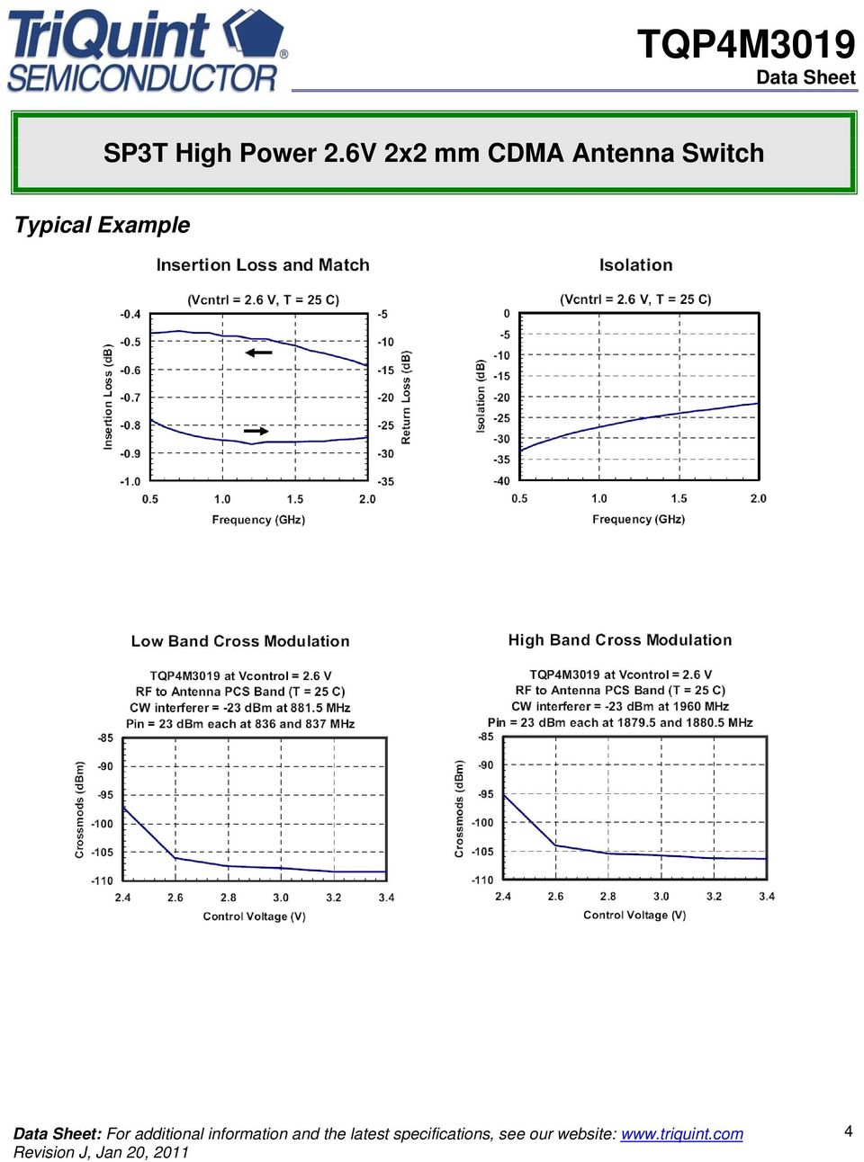
4 Typical Example 4
5 Demonstration Board Circuit Notes: 1. Package Paddle should not be grounded for the best performance. See Application Note for details. 2. RF and DC ground are through pins 1, 6, and 9 3. Control line bypass caps, C2, C5 and C7 should be at least 5pF and may be larger if needed, depending on the switching time required in the application. See Application Note for details. 4. R1, R2 and R3 are optional pull down resistors to ensure the Off legs of the switch are held to a low enough voltage in circuits using open collector style control lines. These lines must be held close to zero volts when the corresponding switch leg is off for proper operation of the switch. A nominal control voltage of +2.6V is applied to V1, V2 or V3 corresponding to the On leg of the switch, with the other two pins held at nominally 0V. Only one switch leg maybe On at any time. 5

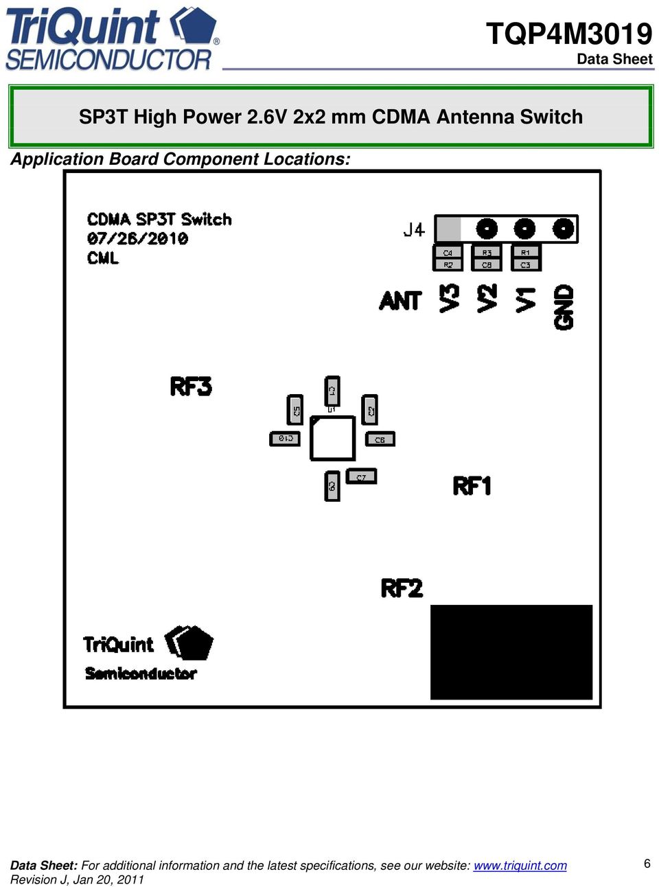
6 Application Board Component Locations: 6
7 Recommended PCB Footprint for 12ld STSLP 2x2x0.57mm Package Procedure: PCB Layout: Leads are to extend away from the pads these should be the same shape and size to ensure equal solder coverage. Solder Mask: The solder mask opening should be offset from the package edges by 250µm. Solder Stencil: Center pad opening is about 30% of PCB pad size. 7

8 Part Marking Information: WHITE INK OR LASER MARK Line 1: 019 Product Code Line 2: XXX Last 3 Char of TriQuint assembly lot number 8

9 Tape and Reel Information: Material will be delivered in packaged form on tape and reel. PART FEATURE SYMBOL SIZE (in) SIZE (mm) CAVITY LENGTH A WIDTH B DEPTH K PITCH P DISTANCE CAVITY TO PERFORATION P BETWEEN CENTERLINE LENGTH DIRECTION CAVITY TO PERFORATION F WIDTH DIRECTION COVER TAPE WIDTH C CARRIER TAPE WIDTH W CAVITY BOTTOM HOLE DIAMETER D PERFORATION DIAMETER D PITCH P POSITION E

10 STSLP-12 7 Reel PART FEATURE SYMBOL SIZE (in) SIZE (mm) FLANGE DIAMETER A THICKNESS W SPACE BETWEEN FLANGE W HUB OUTER DIAMETER N ARBOR HOLE DIAMETER C KEY SLIT WIDTH B KEY SLIT DIAMETER D Each reel shall be marked as specified in TriQuint specification 12M05019A73, Section 7. 10

11 Packaging and Ordering Information: Additional Information 1 This part is compliant with RoHS directive (Restrictions on the Use of Certain Hazardous Substances in Electrical and Electronic Equipment). The part is rated Moisture Sensitivity Level at 260 C per JEDEC standard IPC/JEDEC J-STD For the latest specifications, additional product information, worldwide sales and distribution locations and information about TriQuint: Web: Tel: (503) [email protected] Fax: (503) For Technical questions and additional information on specific applications: [email protected] The information provided herein is believed to be reliable. TriQuint assumes no liability for inaccuracies or omissions. TriQuint assumes no responsibility for the use of this information, and all such information shall be entirely at the user s own risk. Prices and specifications are subject to change without notice. No patent rights or licenses to any of the circuits described herein are implied or granted to any third party. TriQuint does not authorize or warrant any TriQuint product for use in life-support devices and/or systems. Copyright 2005 TriQuint Semiconductor, Inc. All rights reserved 11
 615-9000 Email: info_wireless@tqs.com Fax: (503) 615-8902 For Technical questions and additional information on specific applications: Email: info_wireless@tqs.")
SKY13380-350LF: 20 MHz-3.0 GHz High Power SP4T Switch With Decoder
 DATA SHEET SKY13380-350LF: 20 MHz-3.0 GHz High Power SP4T Switch With Decoder Applications GSM/WCDMA/EDGE datacards and handsets Mobile high power switching systems Features Broadband frequency range:
Symbol Parameters Units Frequency Min. Typ. Max. 850 MHz 14.8 16.3 17.8
 Product Description Sirenza Microdevices SGC-689Z is a high performance SiGe HBT MMIC amplifier utilizing a Darlington configuration with a patented active-bias network. The active bias network provides
MASW-000823-12770T. HMIC TM PIN Diode SP2T 13 Watt Switch for TD-SCDMA Applications. Features. Functional Diagram (TOP VIEW)
") Features Exceptional Loss = 0.35 db Avg @ 2025 MHz, 20mA Exceptional Loss = 0.50 db Avg @ 2025 MHz, 20mA Higher - Isolation = 31dB Avg @ 2025 MHz, 20mA Higher RF C.W. Input Power =13 W C.W.(-Ant Port)
Features Exceptional Loss = 0.35 db Avg @ 2025 MHz, 20mA Exceptional Loss = 0.50 db Avg @ 2025 MHz, 20mA Higher - Isolation = 31dB Avg @ 2025 MHz, 20mA Higher RF C.W. Input Power =13 W C.W.(-Ant Port)
MASW-007070-0001TB. GaAs SPST Switch, Absorptive, Single Supply, DC-4.0 GHz. Features. Pin Configuration 1,2,3,4. Description. Ordering Information
 Features Operates DC - 4 GHz on Single Supply ASIC TTL / CMOS Driver Low DC Power Consumption 50 Ohm Nominal Impedance Test Boards are Available Tape and Reel are Available Lead-Free 4 x 6 mm PQFN Package
SKY13370-374LF: 0.5 to 6.0 GHz SPDT Switch, 50 Ω Terminated
 DATA SHEET SKY13370-374LF: 0.5 to 6.0 GHz SPDT Switch, 50 Ω Terminated Applications WiMAX 802.16 RF1 RF2 Dual-band WLANs (802.11 a/b/g/n) LTE/4G systems 50 Ω 50 Ω Features 50 Ω matched RF ports in all
TQP0103 15 W, DC to 4 GHz, GaN Power Transistor
 Applications W-CDMA / LTE Macrocell Base Station Driver Microcell Base Station Small Cell Active Antenna General Purpose Applications 20 Pin 3x4mm QFN Product Features Functional Block Diagram Operating
CLA4607-085LF: Surface Mount Limiter Diode
 DATA SHEET CLA4607-085LF: Surface Mount Limiter Diode Applications Low-loss, high-power limiters Receiver protectors Anode (Pin 1) Anode (Pin 3) Features Low thermal resistance: 55 C/W Typical threshold
23-26GHz Reflective SP4T Switch. GaAs Monolithic Microwave IC in SMD leadless package
 CHS2411-QDG Description GaAs Monolithic Microwave IC in SMD leadless package The CHS2411-QDG (CHS2412-QDG, see Note) is a monolithic reflective SP4T switch in K-Band. Positive supply voltage only is required.
SKYA21012: 20 MHz to 6.0 GHz GaAs SPDT Switch
 DATA SHEET SKYA2112: 2 MHz to 6. GHz GaAs SPDT Switch Automotive Applications INPUT Infotainment Automated toll systems Output1 Output2 Garage door opener 82.11 b/g/n WLAN, Bluetooth systems Wireless control
Product Datasheet P1110 915 MHz RF Powerharvester Receiver
 DESCRIPTION The Powercast P1110 Powerharvester receiver is an RF energy harvesting device that converts RF to DC. Housed in a compact SMD package, the P1110 receiver provides RF energy harvesting and power
SKY16406-381LF: 2.2-2.8 GHz Two-Way, 0 Degrees Power Divider
 DATA SHEET SKY16406-381LF: 2.2-2.8 GHz Two-Way, 0 Degrees Power Divider Applications TD-LTE systems Satellite communications 2.4 GHz ISM band Features Low insertion loss: 0.3 db @ 2.5 GHz High isolation:
TGF3015-SM. Applications. Product Features. Functional Block Diagram. General Description. Pin Configuration
 Applications Military radar Civilian radar Land mobile and military radio communications Test instrumentation Wideband or narrowband amplifiers Jammers Product Features Functional Block Diagram Frequency:
Typical Performance 1. IS-95C ACPR 21.0 - - - dbm WCDMA ACLR - 19.5 18.5 - dbm
 Device Features OIP3 = 45.0 dbm @ 1900 MHz Gain = 15.0 db @ 1900 MHz Output P1 db = 27.5 dbm @ 1900 MHz 50 Ω Cascadable Patented Over Voltage Protection Circuit Lead-free/RoHS-compliant SOT-89 SMT package
MADP-000504-10720T. Non Magnetic MELF PIN Diode
 MADP-54-172T Features High Power Handling Low Loss / Low Distortion Leadless Low Inductance MELF Package Non-Magnetic Surface Mountable RoHS Compliant MSL 1 Package Style 172 Dot Denotes Cathode Description
DATA SHEET SE2425U : 2.4 GHz Bluetooth Power Amplifier IC. Applications. Product Description. Features. Ordering Information
 Applications Bluetooth tm wireless technology (Class 1) USB dongles, PCMCIA, flash cards, Access Points Enhanced data rate Features Integrated input and inter-stage match +25 dbm GFSK Output Power +19.5
13.5-40.5GHz Frequency Multiplier. GaAs Monolithic Microwave IC. Output power (dbm) -10 -15 -20 -25 -30
 -10 -15 -20 -25 -30") Output power (dbm) GaAs Monolithic Microwave IC Description The is a packaged monolithic time three multiplier which integrates input and output buffer. This circuit is a very versatile multiplier for
Output power (dbm) GaAs Monolithic Microwave IC Description The is a packaged monolithic time three multiplier which integrates input and output buffer. This circuit is a very versatile multiplier for
CMOS 5GHz WLAN 802.11a/n/ac RFeIC WITH PA, LNA, AND SPDT
 CMOS 5GHz WLAN 802.11a/n/ac RFeIC WITH PA, LNA, AND SPDT Description RFX8055 is a highly integrated, single-chip, single-die RFeIC (RF Front-end Integrated Circuit) which incorporates key RF functionality
uclamp0541z Ultra Small μclamp 1-Line ESD Protection
 - Z-Pak TM Description μclamp TVS diodes are designed to protect sensitive electronics from damage or latch-up due to ESD. It is designed to replace 2 size multilayer varistors (MLVs) in portable applications
NBB-402. RoHS Compliant & Pb-Free Product. Typical Applications
 Typical Applications Narrow and Broadband Commercial and Military Radio Designs Linear and Saturated Amplifiers 0 RoHS Compliant & Pb-Free Product NBB-402 CASCADABLE BROADBAND GaAs MMIC AMPLIFIER DC TO
SMS7630-061: Surface Mount, 0201 Zero Bias Silicon Schottky Detector Diode
 DATA SHEET SMS7630-061: Surface Mount, 0201 Zero Bias Silicon Schottky Detector Diode Applications Sensitive RF and microwave detector circuits Sampling and mixer circuits High volume wireless systems
MADR-009190-0001TR. Quad Driver for GaAs FET or PIN Diode Switches and Attenuators Rev. 4. Functional Schematic. Features.
 Features High Voltage CMOS Technology Four Channel Positive Voltage Control CMOS device using TTL input levels Low Power Dissipation Low Cost Lead-Free SOIC-16 Plastic Package Halogen-Free Green Mold Compound
MADR-009269-0001TR. Single Driver for GaAs FET or PIN Diode Switches and Attenuators Rev. V1. Functional Schematic. Features.
 Features High Voltage CMOS Technology Complementary Outputs Positive Voltage Control CMOS device using TTL input levels Low Power Dissipation Low Cost Plastic SOIC-8 Package 100% Matte Tin Plating over
SLG7NT4129 PCIE RTD3. Pin Configuration. Features Low Power Consumption Dynamic Supply Voltage RoHS Compliant / Halogen-Free Pb-Free TDFN-12 Package
 General Description Silego SLG7NT4129 is a low power and small form device. The SoC is housed in a 2.5mm x 2.5mm TDFN package which is optimal for using with small devices. Features Low Power Consumption
MADR-009443-0001TR. Quad Driver for GaAs FET or PIN Diode Switches and Attenuators. Functional Schematic. Features. Description. Pin Configuration 2
 Features Functional Schematic High Voltage CMOS Technology Four Channel Positive Voltage Control CMOS device using TTL input levels Low Power Dissipation Low Cost 4x4 mm, 20-lead PQFN Package 100% Matte
Analog Devices Welcomes Hittite Microwave Corporation NO CONTENT ON THE ATTACHED DOCUMENT HAS CHANGED
 Analog Devices Welcomes Hittite Microwave Corporation NO CONTENT ON THE ATTACHED DOCUMENT HAS CHANGED www.analog.com www.hittite.com THIS PAGE INTENTIONALLY LEFT BLANK v2.71 HMC42ST8 / 42ST8E AMPLIFIER,.4-2.2
Heterojunction Bipolar Transistor Technology (InGaP HBT) Broadband High Linearity Amplifier
 Broadband High Linearity Amplifier") Freescale Semiconductor Technical Data Heterojunction Bipolar Transistor Technology (InGaP HBT) Broadband High Linearity Amplifier The is a general purpose amplifier that is input and output internally
Freescale Semiconductor Technical Data Heterojunction Bipolar Transistor Technology (InGaP HBT) Broadband High Linearity Amplifier The is a general purpose amplifier that is input and output internally
Analog Devices Welcomes Hittite Microwave Corporation NO CONTENT ON THE ATTACHED DOCUMENT HAS CHANGED
 Analog Devices Welcomes Hittite Microwave Corporation NO CONTENT ON THE ATTACHED DOCUMENT HAS CHANGED www.analog.com www.hittite.com THIS PAGE INTENTIONALLY LEFT BLANK Typical Applications The HMC547LP3
Miniature Surface-Mount DAA for Audio or Data Transfer XE0402LCC BLOCK DIAGRAM
 XE0402LCC January 2007 Miniature Surface-Mount DAA for Audio or Data Transfer Description The XE0402LCC supplies a complete telephone line interface or DAA (Data Access Arrangement) in a miniature, surface-mount
Monolithic Amplifier PMA2-43LN+ Ultra Low Noise, High IP3. 50Ω 1.1 to 4.0 GHz. The Big Deal
 Ultra Low Noise, High IP3 Monolithic Amplifier 50Ω 1.1 to 4.0 GHz The Big Deal Ultra low noise figure, 0.46 db High gain, high IP3 Small size, 2 x 2 x 1mm 2mm x 2mm Product Overview Mini-Circuits is an
RF Power LDMOS Transistors Enhancement--Mode Lateral MOSFETs
 Freescale Semiconductor Technical Data RF Power LDMOS Transistors Enhancement--Mode Lateral MOSFETs These 90 W RF power LDMOS transistors are designed for wideband RF power amplifiers covering the frequency
Parameter Min. Typ. Max. Units. Frequency Range 30 50 GHz. Minimum Insertion Loss 1.9 4.7 db. Dynamic Range @ 38 GHz 26 db
 EWA51ZZ 3-5 GHz GaAs MMIC September 29 Rev 4 Bare Die Features Broadband Performance: 3 to 5 GHz Dynamic Range: 26 db, typical Input IP3: +13 dbm, typical (any attenuation) Dual Voltage Control: -1.5 to
Features. Modulation Frequency (khz) VDD. PLL Clock Synthesizer with Spread Spectrum Circuitry GND
 VDD. PLL Clock Synthesizer with Spread Spectrum Circuitry GND") DATASHEET IDT5P50901/2/3/4 Description The IDT5P50901/2/3/4 is a family of 1.8V low power, spread spectrum clock generators capable of reducing EMI radiation from an input clock. Spread spectrum technique
DATASHEET IDT5P50901/2/3/4 Description The IDT5P50901/2/3/4 is a family of 1.8V low power, spread spectrum clock generators capable of reducing EMI radiation from an input clock. Spread spectrum technique
DPDT SWITCH FOR 2.4 GHz AND 6 GHz DUAL-BAND WIRELESS LAN
 GaAs INTEGRATED CIRCUIT PG2164T5N DPDT SWITCH FOR 2.4 GHz AND 6 GHz DUAL-BAND WIRELESS LAN DESCRIPTION The PG2164T5N is a GaAs MMIC DPDT (Double Pole Double Throw) switch which was developed for 2.4 GHz
Broadband covering primary wireless communications bands: Cellular, PCS, LTE, WiMAX
 Ultra Linear Low Noise Monolithic Amplifier 50Ω The Big Deal 0.05 to 4 GHz Ultra High IP3 Broadband High Dynamic Range without external Matching Components May be used as a replacement for RFMD SPF-5189Z
Broadband covering primary wireless communications bands: Cellular, PCS, LTE, WiMAX
 High Gain, High IP3 Monolithic Amplifier 50Ω 0.01 to 6 GHz The Big Deal High Gain Broadband High Dynamic Range without external Matching Components May be used as a replacement to RFMD SBB5089Z a,b SOT-89
XX1007-QT-EV1. Doubler 13.5-17.0/27.0-34.0 GHz. Features. Functional Block Diagram. Description. Pin Configuration. Absolute Maximum Ratings
 XX17-QT 13.-17./27.-34. GHz Features Integrated Gain, and Driver Stages Single Positive Supply, +V Integrated Bypassing Capacitor +2. dbm Output Saturated Power 3. dbc Fundamental Suppression On-Chip ESD
Medium power Schottky barrier single diode
 Rev. 03 17 October 2008 Product data sheet 1. Product profile 1.1 General description Planar medium power Schottky barrier single diode with an integrated guard ring for stress protection, encapsulated
Product Description. Ordering Information. GaAs HBT GaAs MESFET InGaP HBT
 Basestation Applications Cellular and PCS Systems CDMA, W-CDMA Systems GSM/EDGE Systems Final PA for Low-Power Applications RF3223Low Noise, Linear Amplifier High Linearity/Driver Amplifier RF3223 LOW
Metal-Oxide Varistors (MOVs) Surface Mount Multilayer Varistors (MLVs) > MLN Series. MLN SurgeArray TM Suppressor. Description
 Surface Mount Multilayer Varistors (MLVs) > MLN Series. MLN SurgeArray TM Suppressor. Description") MLN SurgeArray TM Suppressor RoHS Description The MLN SurgeArray Suppressor is designed to help protect components from transient voltages that exist at the circuit board level. This device provides four
MLN SurgeArray TM Suppressor RoHS Description The MLN SurgeArray Suppressor is designed to help protect components from transient voltages that exist at the circuit board level. This device provides four
STF203-15 THRU STF203-33
 Description The STF03 is a combination EMI filter and line termination device with integrated diodes for use on upstream USB ports. It is constructed using a proprietary technology that allows passive
Product Specification PE9304
 PE9304 Product Description The PE9304 is a high-performance UltraCMOS prescaler with a fixed divide ratio of 2. Its operating frequency range is 1000 7000 MHz. The PE9304 operates on a nominal 3V supply
PDS5100H. Product Summary. Features and Benefits. Mechanical Data. Description and Applications. Ordering Information (Note 5) Marking Information
 Marking Information") Green 5A HIGH VOLTAGE SCHOTTKY BARRIER RECTIFIER POWERDI 5 Product Summary I F V R V F MAX (V) I R MAX (ma) (V) (A) @ +25 C @ +25 C 1 5..71.35 Description and Applications This Schottky Barrier Rectifier
Green 5A HIGH VOLTAGE SCHOTTKY BARRIER RECTIFIER POWERDI 5 Product Summary I F V R V F MAX (V) I R MAX (ma) (V) (A) @ +25 C @ +25 C 1 5..71.35 Description and Applications This Schottky Barrier Rectifier
SKY65249-11: WLAN 802.11b, g, n Intera Front-End Module
 DATA SHEET SKY69-: WLAN 8.b, g, n Intera Front-End Module Features. to. GHz operation Cardbus, mini PC, PCIe and AP applications POUT @.% EVM (OFDM): 8 dbm Gain: db Integrated PA, filters, directional
Dual-Host / Dual-SIM Card Crosspoint Analog Switch
 FSA2866 Dual-Host / Dual-SIM Card Crosspoint Analog Switch Features Switch Type 2x2 Crosspoint Switch Input Type Data Input Signal Range 0 to V CC V CC 1.65V to 4.30V R ON Data 2Ω (Typical) VSIM 2Ω (Typical)
ICS650-44 SPREAD SPECTRUM CLOCK SYNTHESIZER. Description. Features. Block Diagram DATASHEET
 DATASHEET ICS650-44 Description The ICS650-44 is a spread spectrum clock synthesizer intended for video projector and digital TV applications. It generates three copies of an EMI optimized 50 MHz clock
MAPD-007530-0001TB. Low Cost Two-Way GMIC SMT Power Divider 1700 2000 MHz Rev. V2. Features. Functional Diagram. Description. Ordering Information
 Features Small Size and Low Profile Typical Insertion Loss: 0.6 db Typical Amplitude Balance: 0.2 db 1 Watt Power Handling Lead-Free SOT-26 Package 100% Matte Tin Plating over Copper Halogen-Free Green
SKY66100-11: 169 to 170 MHz Transmit/Receive Front-End Module
 DATA SHEET SKY66100-11: 169 to 170 MHz Transmit/Receive Front-End Module Applications Automated meter reading Advanced metering infrastructure ISM systems Features Transmit output power: >+27 High efficiency
VCC1,2. H/L Lin. Bias, Enable, Detector Circuits
 Applications DSSS 5 GHz WLAN (IEEE802.11an) Access Points, PCMCIA, PC cards Features 5GHz Matched 22dBm Power Amplifier Integrated power amplifier enable pin (VEN) Buffered, temperature compensated power
Data Sheet, V1.1, May 2008 SMM310. Silicon MEMS Microphone. Small Signal Discretes
 Data Sheet, V1.1, May 2008 SMM310 Small Signal Discretes Edition 2008-05-28 Published by Infineon Technologies AG 81726 München, Germany Infineon Technologies AG 2008. All Rights Reserved. Legal Disclaimer
SiGe:C Low Noise High Linearity Amplifier
 Rev. 2 21 February 2012 Product data sheet 1. Product profile 1.1 General description The is a low noise high linearity amplifier for wireless infrastructure applications. The LNA has a high input and
50 ohm nominal input / conjugate match balun to nrf51822- CEAA/CDAB/CFAC and nrf51422-ceaa/cdab/cfac. Benefits. Description
 50 ohm nominal input / conjugate match balun to nrf51822- /CDAB/CFAC and nrf51422-/cdab/cfac Datasheet production data Benefits Very low profile: < 560 µm after reflow High RF performance RF BOM and area
MITSUBISHI RF MOSFET MODULE RA07H4047M
 MITSUBISHI RF MOSFET MODULE RA7H7M RoHS Compliance,-7MHz 7W.V, Stage Amp. For PORTABLE RADIO DESCRIPTION The RA7H7M is a 7-watt RF MOSFET Amplifier Module for.-volt portable radios that operate in the
Supertex inc. HV256. 32-Channel High Voltage Amplifier Array HV256. Features. General Description. Applications. Typical Application Circuit
 32-Channel High Voltage Amplifier Array Features 32 independent high voltage amplifiers 3V operating voltage 295V output voltage 2.2V/µs typical output slew rate Adjustable output current source limit
How To Make An Electric Static Discharge (Esd) Protection Diode
 Protection Diode") Rev. 01 0 October 2008 Product data sheet 1. Product profile 1.1 General description Ultra low capacitance bidirectional ElectroStatic Discharge (ESD) protection diodes in small Surface-Mounted Device
Rev. 01 0 October 2008 Product data sheet 1. Product profile 1.1 General description Ultra low capacitance bidirectional ElectroStatic Discharge (ESD) protection diodes in small Surface-Mounted Device
STRAFT-P98L15. Antenna tuner for cellular application. Features. Description. Applications. Benefits
 Antenna tuner for cellular application Datasheet production data Features 50 nominal Input for a wide range of output impedances Wide operating frequency range (824 MHz to 2170 MHz) Specifically optimized
MAAD-007084-0001TB. Digital Attenuator 15.5 db, 5-Bit, TTL Driver, DC-2.0 GHz Rev. V2. Features. Schematic with Off-Chip Components.
 MAAD-007084-00000 5.5, 5-Bit, TTL Driver, DC-2.0 GHz Rev. 2 Features Attenuation: 0.5 Steps to 5.5 Low DC Power Consumption Integral TTL Driver 50 ohm Impedance Test Boards are Available Tape and Reel
STF201-22 & STF201-30
 Description The STF201 is a combination EMI filter and line termination device with integrated TVS diodes for use on downstream USB ports. It is constructed using a proprietary technology that allows passive
RF Power Field Effect Transistors N- Channel Enhancement- Mode Lateral MOSFETs
 Technical Data RF Power Field Effect Transistors N- Channel Enhancement- Mode Lateral MOSFETs Designed for GSM and GSM EDGE base station applications with frequencies from 864 to 894 MHz. Suitable for
BIPOLAR ANALOG INTEGRATED CIRCUIT
 DATA SHEET BIPOLAR ANALOG INTEGRATED CIRCUIT μpc8tk SiGe:C LOW NOISE AMPLIFIER FOR GPS/MOBILE COMMUNICATIONS DESCRIPTION The μpc8tk is a silicon germanium carbon (SiGe:C) monolithic integrated circuit
Pin Connections and Package Marking. GUx
 Surface Mount RF PIN Switch Diodes Technical Data HSMP-389x Series HSMP-89x Series Features Unique Configurations in Surface Mount Packages Add Flexibility Save Board Space Reduce Cost Switching Low Capacitance
IP4234CZ6. 1. Product profile. Single USB 2.0 ESD protection to IEC 61000-4-2 level 4. 1.1 General description. 1.2 Features. 1.
 Rev. 01 16 April 2009 Product data sheet 1. Product profile 1.1 General description The is designed to protect Input/Output (I/O) USB 2.0 ports, that are sensitive to capacitive loads, from being damaged
BAS16... Silicon Switching Diode For high-speed switching applications Pb-free (RoHS compliant) package 1) Qualified according AEC Q101 BAS16S BAS16U
 package 1) Qualified according AEC Q101 BAS16S BAS16U") BAS6... Silicon Switching Diode For highspeed switching applications Pbfree (RoHS compliant) package ) Qualified according AEC Q BAS6 BAS6W BAS6L BAS6V BAS6W BAS63W BAS6S BAS6U BAS67L4! $ # " "!,,,!,,!
BAS6... Silicon Switching Diode For highspeed switching applications Pbfree (RoHS compliant) package ) Qualified according AEC Q BAS6 BAS6W BAS6L BAS6V BAS6W BAS63W BAS6S BAS6U BAS67L4! $ # " "!,,,!,,!
RClamp0504P RailClamp Low Capacitance TVS Array
 - RailClamp Description RailClamps are low capacitance TVS arrays designed to protect high speed data interfaces. This series has been specifically designed to protect sensitive components which are connected
1 TO 4 CLOCK BUFFER ICS551. Description. Features. Block Diagram DATASHEET
 DATASHEET 1 TO 4 CLOCK BUFFER ICS551 Description The ICS551 is a low cost, high-speed single input to four output clock buffer. Part of IDT s ClockBlocks TM family, this is our lowest cost, small clock
SPECIFICATION. MAT.03A Embedded Active GPS and Cellular Antenna Assembly and Reference Board
 SPECIFICATION Part Number: MAT.03A Product Name: Features: MAT.03A Embedded Active GPS and Cellular Antenna Assembly and Reference Board 2in1 Embedded Antenna Solution Two SMA(F) connectors for Output
MN5010HS GPS Receiver Module
 1 Description The Micro Modular Technologies MN5010HS Global Positioning System (GPS) Receiver is a complete, 20-channel receiver with high sensitivity that measures only 10mm by 10mm by 1.9mm. It features
HT6P20X Series 2 24 OTP Encoder
 2 24 OTP Encoder Features Operating voltage: 2V~12V Low power consumption Built-in oscillator needs only 5% resistor 2/4 data selectable 2 24 maximum address and data codes Easy interface with an RF or
CAN bus ESD protection diode
 Rev. 04 15 February 2008 Product data sheet 1. Product profile 1.1 General description in a small SOT23 (TO-236AB) Surface-Mounted Device (SMD) plastic package designed to protect two automotive Controller
MICROPOWER, GENERAL-SENSITIVE HALL EFFECT SWITCH
 Description The micro power Omni-polar Effect switch IC designed for portable and battery powered equipment such as cellular phones, PDA s and portable PC s. Based on two sensitive Effect plates and chopper
Product Name Hexa-Band Cellular SMD Antenna GSM / CDMA / DCS / PCS / WCDMA /UMTS /HSDPA / GPRS / EDGE 800 MHz to 2200 MHz
 Anam PA.25a Specification Part No. PA.25a Product Name Anam Hexa-Band Cellular SMD Antenna GSM / CDMA / DCS / PCS / WCDMA /UMTS /HSDPA / GPRS / EDGE 800 MHz to 2200 MHz Feature High Efficiency Multi-Band
TYPICAL APPLICATION CIRCUIT. ORDER INFORMATION SOP-EP 8 pin A703EFT (Lead Free) A703EGT (Green)
 A703EGT (Green)") www.addmtek.com 2 CHANNELS 150mA HIGH VOLTAGE ADJUSTABLE CURRENT REGULATOR DESCRIPTION A703 is a high voltage, adjustable constant current driver for LED applications. Two regulated current ports are designed
www.addmtek.com 2 CHANNELS 150mA HIGH VOLTAGE ADJUSTABLE CURRENT REGULATOR DESCRIPTION A703 is a high voltage, adjustable constant current driver for LED applications. Two regulated current ports are designed
FM Radio Transmitter & Receiver Modules
 FM Radio Transmitter & Receiver Modules T5 / R5 Features MINIATURE SIL PACKAGE FULLY SHIELDED DATA RATES UP TO 128KBITS/S RANGE UPTO 300 METRES SINGLE SUPPLY VOLTAGE INDUSTRY PIN COMPATIBLE QFMT5-434 TEMP
VS-702 Voltage Controlled SAW Oscillator Previous Vectron Model VS-720
 VS-702 Voltage Controlled SAW Oscillator Previous Vectron Model VS-720 VS-702 Description The VS-702 is a SAW Based Voltage Controlled Oscillator that achieves low phase noise and very low jitter performance.
Features. Symbol JEDEC TO-220AB
 Data Sheet June 1999 File Number 2253.2 3A, 5V,.4 Ohm, N-Channel Power MOSFET This is an N-Channel enhancement mode silicon gate power field effect transistor designed for applications such as switching
40 V, 200 ma NPN switching transistor
 Rev. 01 21 July 2009 Product data sheet BOTTOM VIEW 1. Product profile 1.1 General description NPN single switching transistor in a SOT883 (SC-101) leadless ultra small Surface-Mounted Device (SMD) plastic
Antenna Part Number: FR05-S1-R-0-105
 Fractus EZConnect Zigbee, RFID, ISM868/9 Chip Antenna Antenna Part Number: FR5-S1-R--15 This product is protected by at least the following patents PAT. US 7,148,85, US 7,22,822 and other domestic and
VS-500 Voltage Controlled SAW Oscillator
 VS-500 Voltage Controlled SAW Oscillator Features Improved High Performance ASIC Industry Standard Package, 9 x 14 x 4.5 mm Frequencies from 155 MHz to 850 MHz 3.3 V or 5.0 V Operation At 155.52 MHz, Jitter
ZL40221 Precision 2:6 LVDS Fanout Buffer with Glitchfree Input Reference Switching and On-Chip Input Termination Data Sheet
 Features Inputs/Outputs Accepts two differential or single-ended inputs LVPECL, LVDS, CML, HCSL, LVCMOS Glitch-free switching of references On-chip input termination and biasing for AC coupled inputs Six
CLA Series: Silicon Limiter Diode Bondable Chips
 DATA SHEET CLA Series: Silicon Limiter Diode Bondable Chips Applications LNA receiver protection Commercial and defense radar Features Established Skyworks limiter diode process High-power, mid-range,
FM TRANSMITTER & RECEIVER HYBRID MODULES. FM-RTFQ SERIES FM-RRFQ SERIES. Transmitter. Receiver. Applications
 FM Radio Transmitter & Receivers Available as or or 868MHz Transmit Range up to 20m Miniature Packages Data Rate up to 9.6Kbps No Adjustable Components Very Stable Operating Frequency Operates from 20
TSM2N7002K 60V N-Channel MOSFET
 SOT-23 SOT-323 Pin Definition: 1. Gate 2. Source 3. Drain PRODUCT SUMMARY V DS (V) R DS(on) (Ω) I D (ma) 5 @ V GS = 10V 100 60 5.5 @ V GS = 5V 100 Features Low On-Resistance ESD Protection High Speed Switching
RClamp0821P. Ultra-Low Capacitance 1-Line ESD protection. PROTECTION PRODUCTS - RailClamp Description. Features. Mechanical Characteristics
 - RailClamp Description The RailClamp family is a series of ultra low capacitance Transient oltage Suppressors (TS) designed to protect high speed data interfaces. This series has been specifically designed
ESD7484. 4-Line Ultra-Large Bandwidth ESD Protection
 4-Line Ultra-Large Bandwidth ESD Protection Functional Description The ESD7484 chip is a monolithic, application specific discrete device dedicated to ESD protection of the HDMI connection. It also offers
PMEG3005EB; PMEG3005EL
 Rev. 0 29 November 2006 Product data sheet. Product profile. General description Planar Maximum Efficiency General Application (MEGA) Schottky barrier rectifiers with an integrated guard ring for stress
PRTR5V0U2F; PRTR5V0U2K
 Rev. 02 19 February 2009 Product data sheet 1. Product profile 1.1 General description Ultra low capacitance double rail-to-rail ElectroStatic Discharge (ESD) protection devices in leadless ultra small
Silvertel. Ag5200. 1 Features. 2 Description. Power-over-Ethernet Plus Module. IEEE802.3at and IEEE802.3af compliant. Maximum 30W output power
 Silvertel V1.1 November 2012 Datasheet Pb 1 Features IEEE802.3at and IEEE802.3af compliant Maximum 30W output power Dual In-Line (DIL) package size 50.6mm (L) x 30mm (W) Overload, short-circuit and thermal
MAX14760/MAX14762/MAX14764 Above- and Below-the-Rails Low-Leakage Analog Switches
 19-652; Rev 1; 8/12 EVALUATION KIT AVAILABLE MAX1476// General Description The MAX1476// analog switches are capable of passing bipolar signals that are beyond their supply rails. These devices operate
PMEG1020EA. 1. Product profile. 2 A ultra low V F MEGA Schottky barrier rectifier. 1.1 General description. 1.2 Features. 1.
 Rev. 04 30 December 2008 Product data sheet 1. Product profile 1.1 General description Planar Maximum Efficiency General Application (MEGA) Schottky barrier rectifier with an integrated guard ring for
SELECTION GUIDE INPUT CHARACTERISTICS. Voltage set point accuracy. Overall voltage error. Temperature coefficient of output voltage (slope)
") OBSOLETE NMPD0 Series SELECTION GUIDE Order Code Nominal Input Voltage Output Voltage Efficiency (Min.) Power (Max.) V V % W NMPD003C 3. 9.50 NMPD005C 5. 9.5 NMPD0C. 0 0.00 NMPD05C 5. 9 0.00 FEATURES RoHS
OBSOLETE NMPD0 Series SELECTION GUIDE Order Code Nominal Input Voltage Output Voltage Efficiency (Min.) Power (Max.) V V % W NMPD003C 3. 9.50 NMPD005C 5. 9.5 NMPD0C. 0 0.00 NMPD05C 5. 9 0.00 FEATURES RoHS
Spread Spectrum Clock Generator AK8126A
 Features Output Frequency Range: 22.5MHz 32MHz, 45 MHz 64MHz 90MHz 128MHz Configurable Spread Spectrum Modulation: - AKEMD s Original Spread Spectrum Profile - Modulation Ratio: Center Spread: ±0.25%,
DG2731/2732/2733. Low Voltage, 0.4 Ω, Dual SPDT Analog Switch. Vishay Siliconix. RoHS COMPLIANT FEATURES
 Low Voltage, 0.4 Ω, Dual SPDT Analog Switch DG273/2732/2733 DESCRIPTION The DG273/2732/2733 are low voltage, low on-resistance, dual single-pole/double-throw (SPDT) monolithic CMOS analog switches designed
1.0A LOW DROPOUT LINEAR REGULATOR
 1.0A LOW DROPOUT LINEAR REGULATOR Description Pin Assignments The is a low dropout three-terminal regulator with 1.0A output current ability, and the dropout voltage is specified at typical 1.1V at 1.0A
PESDxU1UT series. 1. Product profile. Ultra low capacitance ESD protection diode in SOT23 package. 1.1 General description. 1.
 Rev. 02 20 August 2009 Product data sheet 1. Product profile 1.1 General description Ultra low capacitance ElectroStatic Discharge (ESD) protection diode in a SOT23 (TO-236AB) small SMD plastic package
BAV70... BAV70 BAV70W BAV70S BAV70U. Type Package Configuration Marking BAV70 BAV70S BAV70U BAV70W
 BAV7... Silicon Switching Diode For highspeed switching applications Common cathode configuration BAV7S / U: For orientation in reel see package information below Pbfree (RoHS compliant) package ) Qualified
2-Wire/4-Wire Telephone Line Interface. XE0204 Block Diagram
 XE0204 July 2000 2-Wire/4-Wire Telephone Line Interface Description The XE0204 provides a common telephone interface for networks integrating two and four-wire telephone connections. The XE0204 supplies
USBP01-5M8. ESD protection for enhanced micro USB interface. Features. Applications. Description. Complies with following standards
 USBP01-5M8 ESD protection for enhanced micro USB interface Datasheet production data Features D+/D- and ID lines protection with 7 V low voltage diodes (LV) V BUS line protection with 32 V high voltage
HT6221/HT6222 Multi-Purpose Encoders
 Multi-Purpose Encoders Features Operating voltage: 1.8V~3.5V DOUT with 38kHz carrier for R medium Low standby current Minimum transmission word: one word 55kHz ceramic resonator or crystal 16-bit address
65 V, 100 ma PNP/PNP general-purpose transistor
 Rev. 02 19 February 2009 Product data sheet 1. Product profile 1.1 General description PNP/PNP general-purpose transistor pair in a very small SOT363 (SC-88) Surface-Mounted Device (SMD) plastic package.
NTMS4920NR2G. Power MOSFET 30 V, 17 A, N Channel, SO 8 Features
 NTMS9N Power MOSFET 3 V, 7 A, N Channel, SO Features Low R DS(on) to Minimize Conduction Losses Low Capacitance to Minimize Driver Losses Optimized Gate Charge to Minimize Switching Losses These Devices