AB07 Common Collector PNP Transistor Characteristics. Analog lab Experiment board. Ver 1.0
|
|
|
- Constance Barnett
- 9 years ago
- Views:
Transcription
1 Common Collector PNP Transistor Characteristics Analog lab Experiment board Ver 1.0 QUALITY POLICY To be a Global Provider of Innovative and Affordable Electronic Equipments for Technology Training by enhancing Customer Satisfaction based on Research, Modern manufacturing techniques and continuous improvement in Quality of the products and Services with active participation of employees. An ISO 9001: 2000 company , Electronic Complex, Pardesipura INDORE , India.

2 Tel.: Fax: Web: 2

3 3
4 Common Collector PNP Transistor Characteristics TABLE OF CONTENTS 1.Introduction 4 2. Theory 6 3.Experiment 9 To study the characteristics of PNP transistor in common collector configuration and to evaluate Input resistance, Output resistance, and Current gain. 4.Datasheet 16 5.Warranty 18 6.List of Service Centers 19 7.List of Accessories with 20 4

5 INTRODUCTION is a compact, ready to use Transistor Characteristics experiment board. This is useful for students to plot different characteristics of PNP transistor in common collector configuration and to understand various region of operation of PNP transistor. It can be used as stand alone unit with external DC power supply or can be used with SCIENTECH Analog Lab ST2612 which has built in DC power supply, AC power supply, function generator, modulation generator, continuity tester, toggle switches, and potentiometer. List of Boards : Model AB01 AB02 AB03 AB04 AB05 AB06 AB08 AB09 AB10 AB11 AB14 AB15 AB16 AB17 AB18 AB19 AB20 AB21 AB22 AB23 AB25 AB28 AB29 AB30 AB31 AB32 Name Diode characteristics (Si, Zener, LED) Transistor characteristics (CB NPN) Transistor characteristics (CB PNP) Transistor characteristics (CE NPN) Transistor characteristics (CE PNP) Transistor characteristics (CC NPN) FET characteristics Rectifier Circuits Wheatstone Bridge Maxwell s Bridge Darlington Pair Common Emitter Amplifier Common Collector Amplifier Common Base Amplifier Cascode Amplifier RC-Coupled Amplifier Direct Coupled Amplifier Class a Amplifier Class B Amplifier (push pull emitter follower) Class C Tuned Amplifier Phase Locked Loop (FM Demodulator & Frequency Divider / Multiplier) Multivibrator ( Mono stable / Astable) F-V and V-F Converter V-I and I-V Converter Zener Voltage Regulator Transistor Series Voltage Regulator 5

6 AB33 AB41 AB42 AB43 AB44 AB45 AB51 AB52 AB53 AB54 AB56 AB65 AB66 AB67 AB68 AB80 AB81 AB82 AB83 AB84 AB85 AB88 AB89 AB90 AB91 AB92 AB93 AB96 AB97 AB101 AB102 AB106 Transistor Shunt Voltage Regulator Differential Amplifier (Transistorized) Operational Amplifier (Inverting / Non-inverting / Differentiator) Operational Amplifier (Adder/Scalar) Operational Amplifier (Integrator/ Differentiator) Schmitt Trigger and Comparator Active filters (Low Pass and High Pass) Active Band Pass Filter Notch Filter Tschebyscheff Filter Fiber Optic Analog Link Phase Shift Oscillator Wien Bridge Oscillators Colpitt Oscillator Hartley Oscillator RLC Series and RLC Parallel Resonance Kirchoff s Laws (Kirchhoff s Current Law & Kirchhoff s Voltage Law) Thevenin s and Maximum power Transfer Theorem Reciprocity and Superposition Theorem Tellegen s Theorem Norton s theorem Diode Clipper Diode Clampers Two port network parameter Optical Transducer (Photovoltaic cell) Optical Transducer (Photoconductive cell/ldr) Optical Transducer (PhotoTransistor) Temperature Transducer (RTD & IC335) Temperature Transducer (Thermocouple) DSB Modulator and Demodulator SSB Modulator and Demodulator FM Modulator and Demodulator and many more 6
 Thevenin s and Maximum power Transfer Theorem")
7 THEORY Transistor characteristics are the curves, which represent relationship between different dc currents and voltages of a transistor. These are helpful in studying the operation of a transistor when connected in a circuit. The three important characteristics of a transistor are: 1. Input characteristic. 2. Output characteristic. 3. Constant current transfer characteristic. Input Characteristic : In common collector configuration, it is the curve plotted between the input current (IB) verses input voltage (VBC) for various constant values of output voltage (VEC). This characteristic reveals that for fixed value of output voltage VEC, It is quite different from CB and CE configuration. This different is due to the fact that input voltage VBC is largely determined by the value of VEC. As the base to collector voltage increases, VBE is reduced thereby reducing IB. The approximated plot for input characteristic is shown in fig. 1. Fig. 1 7
 verses input voltage (VBC) for various constant values of output voltage (VEC).")
8 Output Characteristic : This is the curve plotted between the output current IE verses output voltage VCE for various constant values of input current IB. The output characteristic has three basic region of interest as indicated in fig.2 the active region, cutoff region and saturation region. In active region the collector base junction is reverse biased while the base emitter junction is forward biased. This region is normally employed for linear (undistorted) amplifier. In cutoff region the collector base junction and base emitter junction of the transistor both are reverse biased. In this region transistor acts as an OFF switch. In saturation region the collector base junction and base emitter junction of the transistor both are forward biased. In this region transistor acts as an ON switch. Fig. 2 8

9 Constant current transfer Characteristic : This is the curve plotted between output emitter current IE verses input base current IB for constant value of output voltage VCE. The approximated plot for this characteristic is shown in Fig 3. Fig. 3 9

10 EXPERIMENT Objective : To study the characteristics of PNP transistor in common collector configuration and to evaluate 1. Input resistance 2. Output resistance 3. Current gain Apparatus required : 1. Analog board of. 2. DC power supplies +12V, -5V from external source or ST2612 Analog Lab. 3. Digital Multimeter (3 numbers) mm patch cords. Circuit diagram : Circuit used to plot different characteristics of transistor is shown in Fig 4. 10

11 Fig. 4 11

12 Procedure : Connect -5V and +12V dc power supplies at their indicated position from external source or ST2612 Analog Lab. To plot input characteristics proceed as follows : 1. Rotate both the potentiometer P1 and P2 fully in CCW (counter clockwise direction). 2. Connect Ammeter between test point 2 and 3 to measure input base current IB(uA). 3. Short or connect a 2mm patch cord between test point 4 and 5 4. Connect one voltmeter between test point 1 and ground to measure input voltage VCB and other voltmeter between test point 6 and ground to measure output voltage VCE. 5. Switch ON the power supply. 6. Vary potentiometer P2 and set a value of output voltage VCE at some constant value (4.5V, 5V, ) 7. Vary the potentiometer P1 so as to increase the value of input voltage VCB in step and measure the corresponding values of input current I B for different constant value of output voltage VCE in an observation Table Rotate potentiometer P1 fully in CCW direction. 9. Repeat the procedure from step 6 for different sets of output voltage VEC. 10. Plot a curve between input voltages VBC and input current IB as shown in Fig 1 using suitable scale with the help of observation Table l. This curve is the required input characteristic. 12
 7.")
13 Observation Table 1 : S.no. Input voltage VBC V V V V V V V V V V Input current IB(uA) at constant value of output voltage VEC = 4.5V VEC = 5V VEC =5.5V To plot output characteristics proceed as follows : 1. Switch OFF the power supply. 2. Rotate both the potentiometer P1 and P2 fully in CCW (counter clockwise direction). 3. Connect voltmeter between test point 6 and ground to measure output voltage VEC. 4. Connect one Ammeter between test point 2 and 3 to measure input current IB(uA) and other Ammeter between test point 4 and 5 to measure output current IE(mA). 5. Switch ON the power supply. 6. Vary potentiometer P1 and set a value of input current IB at some constant value (0uA i.e. input open circuit/remove ammeter between test point 2 and 3, 1uA, 2uA...) 13
 and other Ammeter between test point 4 and 5 to measure output current IE(mA). 5. Switch ON the power supply. 6.")
14 7. Vary the potentiometer P2 so as to increase the value of output voltage VEC from zero to maximum value in step and measure the corresponding values of output current IE for different constant value of input current IB in an observation table Rotate potentiometer P2 fully in CCW direction. 9. Repeat the procedure from step 6 for different sets of input current IB. 10. Plot a curve between output voltage VEC and output current IE as shown in Fig 2 using suitable scale with the help of observation table 2. This curve is the required output characteristic. Observation Table 2 : Output current IE (ma) at constant value of Output input voltage S.no. voltage IB = 0uA VCE IB =10uA IB =20uA IB =30uA IB =40uA (open) V V V V V V V V V To plot constant current transfer characteristics proceed as follows: 1. Switch OFF the power supply. 2. Rotate both the potentiometer P1 and P2 fully in CCW (counter clockwise direction). 14
 at constant value of Output input voltage S.no. voltage IB = 0uA VCE IB =10uA IB =20uA IB =30uA IB =40uA (open) 1. 0.0V 2. 0.5V 3. 1.0V 4. 2.0V 5. 3.0V 6.")
15 3. Connect voltmeter between test point 6 and ground to measure output voltage VCE. 4. Connect one Ammeter between test point 2 and 3 to measure input current IB (ma) and other Ammeter between test point 4 and 5 to measure output current IE (ma). 5. Switch ON the power supply. 6. Vary potentiometer P2 and set a value of output voltage VCE at constant value. 7. Vary the potentiometer P1 so as to increase the value of input current IB in step and measure the corresponding values of output current IE in an observation Table Plot a curve between output current IE and input current IB as shown in Fig 3 using suitable scale with the help of observation Table 3. This curve is the required Transfer characteristic. Observation Table 3 : S.no. Input current IB (ua) Output current IE (ma) at constant output voltage VEC = 3V

16 16

17 Calculations : 1. Input resistance: It is the ratio of change in the input voltage VBC to change in the input current IB at constant value of output voltage VEC or it is the reciprocal of the slope obtained from the input characteristic. Mathematically To calculate input resistance determine the slope from the input characteristic curve obtained from observation Table 1. Reciprocal of this slope will give the required input resistance. 2. Output resistance: It is the ratio of change in the output voltage VEC to change in the output current IE at constant value of input current IB or it is the reciprocal of the slope obtained from the output characteristic. Mathematically To calculate output resistance determine the slope from the output characteristic curve obtained from observation Table 2. Reciprocal of this slope will give the required output resistance. 3. Current gain: It is the ratio of change in the output current I E to change in the input current IB at constant value of output voltage VEC or it is the slope obtained from the constant current transfer characteristic. It is denoted by αac 17

18 Mathematically αac = Slope of constant current transfer characteristic = IE IB To calculate current gain, determine the slope from the constant current transfer characteristic curve obtained from observation Table 3. This slope is the required current gain. Results : Input resistance Rin = Output resistance Rout = Current Gain αac = 18

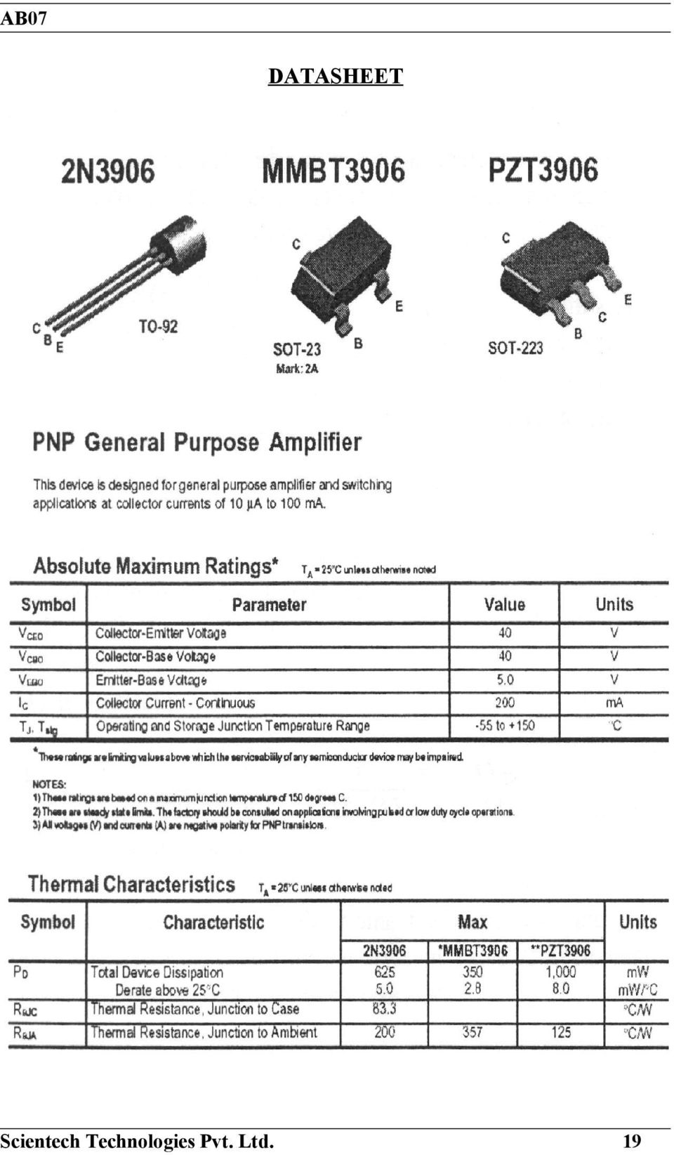
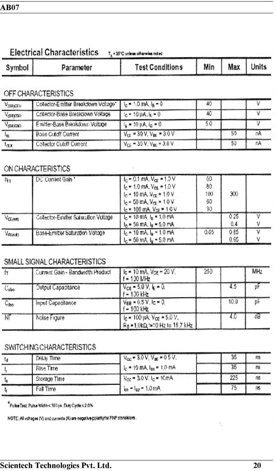
19 DATASHEET 19
20 20
21 WARRANTY 1) We guarantee the instrument against all manufacturing defects during 24 months from the date of sale by us or through our dealers. 2) The guarantee covers manufacturing defects in respect of indigenous components and material limited to the warranty extended to us by the original manufacturer, and defect will be rectified as far as lies within our control. 3) The guarantee will become INVALID. a) If the instrument is not operated as per instruction given in the instruction manual. b) If the agreed payment terms and other conditions of sale are not followed. c) If the customer resells the instrument to another party. d) Provided no attempt have been made to service and modify the instrument. 4) The non-working of the instrument is to be communicated to us immediately giving full details of the complaints and defects noticed specifically mentioning the type and sr. no. of the instrument, date of purchase etc. 5) The repair work will be carried out, provided the instrument is dispatched securely packed and insured with the railways. To and fro charges will be to the account of the customer. DESPATCH PROCEDURE FOR SERVICE Should it become necessary to send back the instrument to factory please observe the following procedure: 1) Before dispatching the instrument please write to us giving fully details of the fault noticed. 2) After receipt of your letter our repairs dept. will advise you whether it is necessary to send the instrument back to us for repairs or the adjustment is possible in your premises. Dispatch the instrument (only on the receipt of our advice) securely packed in original packing duly insured and freight paid along with accessories and a copy of the details noticed to us at our factory address. 21
22 LIST OF SERVICE CENTERS 1. 90, Electronic Complex Pardesipura, INDORE First Floor, C-19, F.I.E., Patparganj Industrial Area, DELHI New no.2, Old no.10, 4th street Venkateswara nagar, Adyar CHENNAI /19, 4th main street Ganganagar, BANGALORE ,1st floor, 123-Hariram Mansion, Dada Saheb Phalke road, Dadar (East), MUMBAI , Sadashiv Peth, Gyan Prabodhini Lane, PUNE Scientech Technologies Pvt. Ltd SPS Apartment, 1st Floor 2, Ahmed Mamoji Street, Behind Jaiswal Hospital, Liluah, HOWRAH W.B. 8. Scientech Technologies Pvt. Ltd Flat No. 205, 2nd Floor, Lakshminarayana Apartments C wing, Street No. 17, Himaytnagar, HYDERABAD Ph : (0731) [email protected] Ph : (011) , Fax : (011) [email protected] Ph : (044) , Fax : (044) [email protected] Ph : (080) Fax : (080) [email protected] Ph : (022) Fax : (022) [email protected] Ph : (020) Fax : (020) [email protected] Ph : [email protected] Ph : (040) [email protected] 22
23 LIST OF ACCESSORIES 1. 2mm Patch cord (red)...2 Nos. 2. 2mm Patch cord (black)...2 Nos. 3. 2mm Patch cord (blue)...1 Nos. 23
Operating Manual Ver.1.1
 Class B Amplifier (Push-Pull Emitter Follower) Operating Manual Ver.1.1 An ISO 9001 : 2000 company 94-101, Electronic Complex Pardesipura, Indore- 452010, India Tel : 91-731- 2570301/02, 4211100 Fax: 91-731-
Operating Manual Ver.1.1
 Silicon, Zener, LED Diode Characteristics Operating Manual Ver.1.1 An ISO 9001 : 2000 company 94-101, Electronic Complex Pardesipura, Indore- 452010, India Tel : 91-731- 2570301/02, 4211100 Fax: 91-731-
DB19. 4-Bit Parallel Adder/ Subtractor. Digital Lab Experiment Board Ver. 1.0
 4-Bit Parallel Adder/ Subtractor Digital Lab Experiment Board Ver. 1.0 QUALITY POLICY To be a Global Leader of Innovative, Competitive and Eco friendly Electronic Equipment, Software Products and Turn-key
Operating Manual Ver.1.1
 4 Bit Binary Ripple Counter (Up-Down Counter) Operating Manual Ver.1.1 An ISO 9001 : 2000 company 94-101, Electronic Complex Pardesipura, Indore- 452010, India Tel : 91-731- 2570301/02, 4211100 Fax: 91-731-
Unit/Standard Number. High School Graduation Years 2010, 2011 and 2012
 1 Secondary Task List 100 SAFETY 101 Demonstrate an understanding of State and School safety regulations. 102 Practice safety techniques for electronics work. 103 Demonstrate an understanding of proper
Content Map For Career & Technology
 Content Strand: Applied Academics CT-ET1-1 analysis of electronic A. Fractions and decimals B. Powers of 10 and engineering notation C. Formula based problem solutions D. Powers and roots E. Linear equations
DEGREE: Bachelor in Biomedical Engineering YEAR: 2 TERM: 2 WEEKLY PLANNING
 SESSION WEEK COURSE: Electronic Technology in Biomedicine DEGREE: Bachelor in Biomedical Engineering YEAR: 2 TERM: 2 WEEKLY PLANNING DESCRIPTION GROUPS (mark X) SPECIAL ROOM FOR SESSION (Computer class
Transistor Amplifiers
 Physics 3330 Experiment #7 Fall 1999 Transistor Amplifiers Purpose The aim of this experiment is to develop a bipolar transistor amplifier with a voltage gain of minus 25. The amplifier must accept input
Bipolar Transistor Amplifiers
 Physics 3330 Experiment #7 Fall 2005 Bipolar Transistor Amplifiers Purpose The aim of this experiment is to construct a bipolar transistor amplifier with a voltage gain of minus 25. The amplifier must
REPORT ON CANDIDATES WORK IN THE CARIBBEAN ADVANCED PROFICIENCY EXAMINATION MAY/JUNE 2008 ELECTRICAL AND ELECTRONIC TECHNOLOGY (TRINIDAD AND TOBAGO)
") CARIBBEAN EXAMINATIONS COUNCIL REPORT ON CANDIDATES WORK IN THE CARIBBEAN ADVANCED PROFICIENCY EXAMINATION MAY/JUNE 2008 ELECTRICAL AND ELECTRONIC TECHNOLOGY (TRINIDAD AND TOBAGO) Copyright 2008 Caribbean
CARIBBEAN EXAMINATIONS COUNCIL REPORT ON CANDIDATES WORK IN THE CARIBBEAN ADVANCED PROFICIENCY EXAMINATION MAY/JUNE 2008 ELECTRICAL AND ELECTRONIC TECHNOLOGY (TRINIDAD AND TOBAGO) Copyright 2008 Caribbean
Basic Electronics Prof. Dr. Chitralekha Mahanta Department of Electronics and Communication Engineering Indian Institute of Technology, Guwahati
 Basic Electronics Prof. Dr. Chitralekha Mahanta Department of Electronics and Communication Engineering Indian Institute of Technology, Guwahati Module: 2 Bipolar Junction Transistors Lecture-2 Transistor
Amplifier Teaching Aid
 Amplifier Teaching Aid Table of Contents Amplifier Teaching Aid...1 Preface...1 Introduction...1 Lesson 1 Semiconductor Review...2 Lesson Plan...2 Worksheet No. 1...7 Experiment No. 1...7 Lesson 2 Bipolar
Physics 623 Transistor Characteristics and Single Transistor Amplifier Sept. 13, 2006
 Physics 623 Transistor Characteristics and Single Transistor Amplifier Sept. 13, 2006 1 Purpose To measure and understand the common emitter transistor characteristic curves. To use the base current gain
Transistor Characteristics and Single Transistor Amplifier Sept. 8, 1997
 Physics 623 Transistor Characteristics and Single Transistor Amplifier Sept. 8, 1997 1 Purpose To measure and understand the common emitter transistor characteristic curves. To use the base current gain
Bipolar Junction Transistors
 Bipolar Junction Transistors Physical Structure & Symbols NPN Emitter (E) n-type Emitter region p-type Base region n-type Collector region Collector (C) B C Emitter-base junction (EBJ) Base (B) (a) Collector-base
POWER SUPPLY MODEL XP-15. Instruction Manual ELENCO
 POWER SUPPLY MODEL XP-15 Instruction Manual ELENCO Copyright 2013 by Elenco Electronics, Inc. REV-A 753020 All rights reserved. No part of this book shall be reproduced by any means; electronic, photocopying,
ELABOTrainingsSysteme Aus- und Weiterbildung GmbH. Electrical Engineering Electronics Digital Technology. www.elabo-ts.com
 Aus- und Weiterbildung GmbH Electrical Engineering Electronics Digital Technology www.elabo-ts.com Principles of Electrical Engineering... Analysis of electrical-engineering systems on component level
Transistor Biasing. The basic function of transistor is to do amplification. Principles of Electronics
 192 9 Principles of Electronics Transistor Biasing 91 Faithful Amplification 92 Transistor Biasing 93 Inherent Variations of Transistor Parameters 94 Stabilisation 95 Essentials of a Transistor Biasing
Bipolar Junction Transistor Basics
 by Kenneth A. Kuhn Sept. 29, 2001, rev 1 Introduction A bipolar junction transistor (BJT) is a three layer semiconductor device with either NPN or PNP construction. Both constructions have the identical
OPERATIONAL AMPLIFIER
 MODULE3 OPERATIONAL AMPLIFIER Contents 1. INTRODUCTION... 3 2. Operational Amplifier Block Diagram... 3 3. Operational Amplifier Characteristics... 3 4. Operational Amplifier Package... 4 4.1 Op Amp Pins
BSNL TTA Question Paper-Instruments and Measurement Specialization 2007
 BSNL TTA Question Paper-Instruments and Measurement Specialization 2007 (1) Instrument is a device for determining (a) the magnitude of a quantity (b) the physics of a variable (c) either of the above
The 2N3393 Bipolar Junction Transistor
 The 2N3393 Bipolar Junction Transistor Common-Emitter Amplifier Aaron Prust Abstract The bipolar junction transistor (BJT) is a non-linear electronic device which can be used for amplification and switching.
LM 358 Op Amp. If you have small signals and need a more useful reading we could amplify it using the op amp, this is commonly used in sensors.
 LM 358 Op Amp S k i l l L e v e l : I n t e r m e d i a t e OVERVIEW The LM 358 is a duel single supply operational amplifier. As it is a single supply it eliminates the need for a duel power supply, thus
Electronics. Discrete assembly of an operational amplifier as a transistor circuit. LD Physics Leaflets P4.2.1.1
 Electronics Operational Amplifier Internal design of an operational amplifier LD Physics Leaflets Discrete assembly of an operational amplifier as a transistor circuit P4.2.1.1 Objects of the experiment
LABORATORY 2 THE DIFFERENTIAL AMPLIFIER
 LABORATORY 2 THE DIFFERENTIAL AMPLIFIER OBJECTIVES 1. To understand how to amplify weak (small) signals in the presence of noise. 1. To understand how a differential amplifier rejects noise and common
Study Guide for the Electronics Technician Pre-Employment Examination
 Bay Area Rapid Transit District Study Guide for the Electronics Technician Pre-Employment Examination INTRODUCTION The Bay Area Rapid Transit (BART) District makes extensive use of electronics technology
Voltage Divider Bias
 Voltage Divider Bias ENGI 242 ELEC 222 BJT Biasing 3 For the Voltage Divider Bias Configurations Draw Equivalent Input circuit Draw Equivalent Output circuit Write necessary KVL and KCL Equations Determine
VCE Physics and VCE Systems Engineering: Table of electronic symbols
 VCE Physics and VCE Systems Engineering: Table of electronic symbols In response to requests from teachers the VCAA has produced a table of commonly used electronic symbols. Practicing teachers have provided
Transistors. NPN Bipolar Junction Transistor
 Transistors They are unidirectional current carrying devices with capability to control the current flowing through them The switch current can be controlled by either current or voltage ipolar Junction
TRANSISTOR/DIODE TESTER
 TRANSISTOR/DIODE TESTER MODEL DT-100 Lesson Manual ELENCO Copyright 2012, 1988 REV-G 753115 Elenco Electronics, Inc. Revised 2012 FEATURES Diode Mode: 1. Checks all types of diodes - germanium, silicon,
Wires & Connections Component Circuit Symbol Function of Component. Power Supplies Component Circuit Symbol Function of Component
 Lista Dei Simboli Dei Circuiti Per i Componenti Elettronici Wires & Connections Wire Wires joined Wires not joined To pass current very easily from one part of a circuit to another. A 'blob' should be
Lab 1: DC Circuits. Student 1, [email protected] Partner : Student 2, [email protected]
 Lab Date Lab 1: DC Circuits Student 1, [email protected] Partner : Student 2, [email protected] I. Introduction The purpose of this lab is to allow the students to become comfortable with the use of lab
6.101 Final Project Report Class G Audio Amplifier
 6.101 Final Project Report Class G Audio Amplifier Mark Spatz 4/3/2014 1 1 Introduction For my final project, I designed and built a 150 Watt audio amplifier to replace the underpowered and unreliable
Common Base BJT Amplifier Common Collector BJT Amplifier
 Common Base BJT Amplifier Common Collector BJT Amplifier Common Collector (Emitter Follower) Configuration Common Base Configuration Small Signal Analysis Design Example Amplifier Input and Output Impedances
Regulated D.C. Power Supply
 442 17 Principles of Electronics Regulated D.C. Power Supply 17.1 Ordinary D.C. Power Supply 17.2 Important Terms 17.3 Regulated Power Supply 17.4 Types of Voltage Regulators 17.5 Zener Diode Voltage Regulator
LAB VIII. BIPOLAR JUNCTION TRANSISTOR CHARACTERISTICS
 LAB VIII. BIPOLAR JUNCTION TRANSISTOR CHARACTERISTICS 1. OBJECTIVE In this lab, you will study the DC characteristics of a Bipolar Junction Transistor (BJT). 2. OVERVIEW In this lab, you will inspect the
W04 Transistors and Applications. Yrd. Doç. Dr. Aytaç Gören
 W04 Transistors and Applications W04 Transistors and Applications ELK 2018 - Contents W01 Basic Concepts in Electronics W02 AC to DC Conversion W03 Analysis of DC Circuits (self and condenser) W04 Transistors
LAB VII. BIPOLAR JUNCTION TRANSISTOR CHARACTERISTICS
 LAB VII. BIPOLAR JUNCTION TRANSISTOR CHARACTERISTICS 1. OBJECTIVE In this lab, you will study the DC characteristics of a Bipolar Junction Transistor (BJT). 2. OVERVIEW You need to first identify the physical
BJT Characteristics and Amplifiers
 BJT Characteristics and Amplifiers Matthew Beckler [email protected] EE2002 Lab Section 003 April 2, 2006 Abstract As a basic component in amplifier design, the properties of the Bipolar Junction Transistor
GUJARAT TECHNOLOGICAL UNIVERSITY, AHMEDABAD, GUJARAT. Course Curriculum. ELECTRONIC COMPONENTS AND CIRCUITS (Code: 3330905) Electrical Engineering
 Electrical Engineering") GUJARAT TECHNOLOGICAL UNIVERSITY, AHMEDABAD, GUJARAT Course Curriculum ELECTRONIC COMPONENTS AND CIRCUITS (Code: 3330905) Diploma Programme in which this course is offered Semester in which offered Electrical
GUJARAT TECHNOLOGICAL UNIVERSITY, AHMEDABAD, GUJARAT Course Curriculum ELECTRONIC COMPONENTS AND CIRCUITS (Code: 3330905) Diploma Programme in which this course is offered Semester in which offered Electrical
AMPLIFIERS BJT BJT TRANSISTOR. Types of BJT BJT. devices that increase the voltage, current, or power level
 AMPLFERS Prepared by Engr. JP Timola Reference: Electronic Devices by Floyd devices that increase the voltage, current, or power level have at least three terminals with one controlling the flow between
Series-Parallel Circuits. Objectives
 Series-Parallel Circuits Objectives Identify series-parallel configuration Analyze series-parallel circuits Apply KVL and KCL to the series-parallel circuits Analyze loaded voltage dividers Determine the
Jeong-Yeol Yoon. Introduction to Biosensors. From Electric Circuits to Immunosensors. f) Springer
 Springer") Jeong-Yeol Yoon Introduction to Biosensors From Electric Circuits to Immunosensors f) Springer Contents 1 Introduction 1 1.1 Sensors 1 1.2 Transducers 2 1.3 Biosensors 4 1.4 Bioreceptors 5 1.5 Transducers
Jeong-Yeol Yoon Introduction to Biosensors From Electric Circuits to Immunosensors f) Springer Contents 1 Introduction 1 1.1 Sensors 1 1.2 Transducers 2 1.3 Biosensors 4 1.4 Bioreceptors 5 1.5 Transducers
ANALOG & DIGITAL ELECTRONICS
 ANALOG & DIGITAL ELECTRONICS Course Instructor: Course No: PH-218 3-1-0-8 Dr. A.P. Vajpeyi E-mail: [email protected] Room No: #305 Department of Physics, Indian Institute of Technology Guwahati,
Guru Ghasidas Vishwavidyalaya, Bilaspur (C.G.) Institute of Technology. Electronics & Communication Engineering. B.
 Institute of Technology. Electronics & Communication Engineering. B.") Guru Ghasidas Vishwavidyalaya, Bilaspur (C.G.) Institute of Technology Electronics & Communication Engineering B.Tech III Semester 1. Electronic Devices Laboratory 2. Digital Logic Circuit Laboratory 3.
Guru Ghasidas Vishwavidyalaya, Bilaspur (C.G.) Institute of Technology Electronics & Communication Engineering B.Tech III Semester 1. Electronic Devices Laboratory 2. Digital Logic Circuit Laboratory 3.
Lecture 12: DC Analysis of BJT Circuits.
 Whites, 320 Lecture 12 Page 1 of 9 Lecture 12: D Analysis of JT ircuits. n this lecture we will consider a number of JT circuits and perform the D circuit analysis. For those circuits with an active mode
Common-Emitter Amplifier
 Common-Emitter Amplifier A. Before We Start As the title of this lab says, this lab is about designing a Common-Emitter Amplifier, and this in this stage of the lab course is premature, in my opinion,
2N6056. NPN Darlington Silicon Power Transistor DARLINGTON 8 AMPERE SILICON POWER TRANSISTOR 80 VOLTS, 100 WATTS
 NPN Darlington Silicon Power Transistor The NPN Darlington silicon power transistor is designed for general purpose amplifier and low frequency switching applications. High DC Current Gain h FE = 3000
Lecture 18: Common Emitter Amplifier. Maximum Efficiency of Class A Amplifiers. Transformer Coupled Loads.
 Whites, EE 3 Lecture 18 Page 1 of 10 Lecture 18: Common Emitter Amplifier. Maximum Efficiency of Class A Amplifiers. Transformer Coupled Loads. We discussed using transistors as switches in the last lecture.
Dependent Sources: Introduction and analysis of circuits containing dependent sources.
 Dependent Sources: Introduction and analysis of circuits containing dependent sources. So far we have explored timeindependent (resistive) elements that are also linear. We have seen that two terminal
Lab 3 - DC Circuits and Ohm s Law
 Lab 3 DC Circuits and Ohm s Law L3-1 Name Date Partners Lab 3 - DC Circuits and Ohm s Law OBJECTIES To learn to apply the concept of potential difference (voltage) to explain the action of a battery in
DIODE CIRCUITS LABORATORY. Fig. 8.1a Fig 8.1b
 DIODE CIRCUITS LABORATORY A solid state diode consists of a junction of either dissimilar semiconductors (pn junction diode) or a metal and a semiconductor (Schottky barrier diode). Regardless of the type,
Table 1 Comparison of DC, Uni-Polar and Bi-polar Stepper Motors
 Electronics Exercise 3: Uni-Polar Stepper Motor Controller / Driver Mechatronics Instructional Laboratory Woodruff School of Mechanical Engineering Georgia Institute of Technology Lab Director: I. Charles
Programmable Single-/Dual-/Triple- Tone Gong SAE 800
 Programmable Single-/Dual-/Triple- Tone Gong Preliminary Data SAE 800 Bipolar IC Features Supply voltage range 2.8 V to 18 V Few external components (no electrolytic capacitor) 1 tone, 2 tones, 3 tones
Diode Circuits. Operating in the Reverse Breakdown region. (Zener Diode)
") Diode Circuits Operating in the Reverse Breakdown region. (Zener Diode) In may applications, operation in the reverse breakdown region is highly desirable. The reverse breakdown voltage is relatively insensitive
Diode Circuits Operating in the Reverse Breakdown region. (Zener Diode) In may applications, operation in the reverse breakdown region is highly desirable. The reverse breakdown voltage is relatively insensitive
Vincennes University ELEC 100- Basic Electricity & Electronics ELEC 110-Basic Component & Circuit Analysis
 Indiana Department of Education Academic Content Framework ELECTRONICS AND COMPUTER TECHNOLOGY I Electronics and Computer Technology I introduces students to the fundamental electronic concepts necessary
Lecture-7 Bipolar Junction Transistors (BJT) Part-I Continued
 Part-I Continued") 1 Lecture-7 ipolar Junction Transistors (JT) Part-I ontinued 1. ommon-emitter (E) onfiguration: Most JT circuits employ the common-emitter configuration shown in Fig.1. This is due mainly to the fact that
1 Lecture-7 ipolar Junction Transistors (JT) Part-I ontinued 1. ommon-emitter (E) onfiguration: Most JT circuits employ the common-emitter configuration shown in Fig.1. This is due mainly to the fact that
Diodes and Transistors
 Diodes What do we use diodes for? Diodes and Transistors protect circuits by limiting the voltage (clipping and clamping) turn AC into DC (voltage rectifier) voltage multipliers (e.g. double input voltage)
Troubleshooting accelerometer installations
 Troubleshooting accelerometer installations Accelerometer based monitoring systems can be tested to verify proper installation and operation. Testing ensures data integrity and can identify most problems.
Vdc. Vdc. Adc. W W/ C T J, T stg 65 to + 200 C
 2N6284 (NPN); 2N6286, Preferred Device Darlington Complementary Silicon Power Transistors These packages are designed for general purpose amplifier and low frequency switching applications. Features High
Op Amp Circuit Collection
 Op Amp Circuit Collection Note: National Semiconductor recommends replacing 2N2920 and 2N3728 matched pairs with LM394 in all application circuits. Section 1 Basic Circuits Inverting Amplifier Difference
Analog & Digital Electronics Course No: PH-218
 Analog & Digital Electronics Course No: PH-18 Lec 3: Rectifier and Clipper circuits Course nstructors: Dr. A. P. VAJPEY Department of Physics, ndian nstitute of Technology Guwahati, ndia 1 Rectifier Circuits:
Frequency Response of Filters
 School of Engineering Department of Electrical and Computer Engineering 332:224 Principles of Electrical Engineering II Laboratory Experiment 2 Frequency Response of Filters 1 Introduction Objectives To
Course: Bachelor of Science (B. Sc.) 1 st year. Subject: Electronic Equipment Maintenance. Scheme of Examination for Semester 1 & 2
 1 st year. Subject: Electronic Equipment Maintenance. Scheme of Examination for Semester 1 & 2") UPDATED SCHEME OF EXAMS. & SYLLABI FOR B.SC. Course: Bachelor of Science (B. Sc.) 1 st year Subject: Electronic Equipment Maintenance Scheme of Examination for Semester 1 & 2 (i) Theory: Two papers of
UPDATED SCHEME OF EXAMS. & SYLLABI FOR B.SC. Course: Bachelor of Science (B. Sc.) 1 st year Subject: Electronic Equipment Maintenance Scheme of Examination for Semester 1 & 2 (i) Theory: Two papers of
3 The TTL NAND Gate. Fig. 3.1 Multiple Input Emitter Structure of TTL
 3 The TTL NAND Gate 3. TTL NAND Gate Circuit Structure The circuit structure is identical to the previous TTL inverter circuit except for the multiple emitter input transistor. This is used to implement
Chapter 19 Operational Amplifiers
 Chapter 19 Operational Amplifiers The operational amplifier, or op-amp, is a basic building block of modern electronics. Op-amps date back to the early days of vacuum tubes, but they only became common
Design and Applications of HCPL-3020 and HCPL-0302 Gate Drive Optocouplers
 Design and Applications of HCPL-00 and HCPL-00 Gate Drive Optocouplers Application Note 00 Introduction The HCPL-00 (DIP-) and HCPL-00 (SO-) consist of GaAsP LED optically coupled to an integrated circuit
Peak Atlas DCA. Semiconductor Component Analyser Model DCA55. User Guide
 GB55-7 Peak Atlas DCA Semiconductor Component Analyser Model DCA55 User Guide Peak Electronic Design Limited 2000/2007 In the interests of development, information in this guide is subject to change without
The basic cascode amplifier consists of an input common-emitter (CE) configuration driving an output common-base (CB), as shown above.
 configuration driving an output common-base (CB), as shown above.") Cascode Amplifiers by Dennis L. Feucht Two-transistor combinations, such as the Darlington configuration, provide advantages over single-transistor amplifier stages. Another two-transistor combination
Cascode Amplifiers by Dennis L. Feucht Two-transistor combinations, such as the Darlington configuration, provide advantages over single-transistor amplifier stages. Another two-transistor combination
Series and Parallel Circuits
 Direct Current (DC) Direct current (DC) is the unidirectional flow of electric charge. The term DC is used to refer to power systems that use refer to the constant (not changing with time), mean (average)
Operating instructions
 Operating instructions Torque transducer type AE with replaceable strain gauge measuring element Model TQ 505 Operating instructions no. 1079 Torque Transducer TQ 505 Page 1 / 16 1. Contents 1. List of
OPERATIONAL AMPLIFIERS. o/p
 OPERATIONAL AMPLIFIERS 1. If the input to the circuit of figure is a sine wave the output will be i/p o/p a. A half wave rectified sine wave b. A fullwave rectified sine wave c. A triangular wave d. A
Understanding Low Drop Out (LDO) Regulators
 Regulators") Understanding Low Drop Out (LDO) Regulators Michael Day, Texas Instruments ABSTRACT This paper provides a basic understanding of the dropout performance of a low dropout linear regulator (LDO). It shows
Understanding Low Drop Out (LDO) Regulators Michael Day, Texas Instruments ABSTRACT This paper provides a basic understanding of the dropout performance of a low dropout linear regulator (LDO). It shows
MAS.836 HOW TO BIAS AN OP-AMP
 MAS.836 HOW TO BIAS AN OP-AMP Op-Amp Circuits: Bias, in an electronic circuit, describes the steady state operating characteristics with no signal being applied. In an op-amp circuit, the operating characteristic
Single Supply Op Amp Circuits Dr. Lynn Fuller
 ROCHESTER INSTITUTE OF TECHNOLOGY MICROELECTRONIC ENGINEERING Single Supply Op Amp Circuits Dr. Lynn Fuller Webpage: http://people.rit.edu/lffeee 82 Lomb Memorial Drive Rochester, NY 146235604 Tel (585)
Automatic Voltage Regulator User s Manual
 Resp. dept. R&D We reserve all rights in this document and in the information contained therein. Reproduction, use or disclosure to third parties without express authority is strictly forbidden. Copyright
Y.LIN ELECTRONICS CO.,LTD.
 Features Current transfer ratio (CTR 50~600% at I F =5mA, V CE =5V) High isolation voltage between input and output (Viso=5000 V rms ) Creepage distance >7.62 mm Operating temperature up to +110 C Compact
STUDY OF CELLPHONE CHARGERS
 STUDY OF CELLPHONE CHARGERS Author : Suraj Hebbar Systems Lab, CeNSE,IISc Banglore ABSTRACT This report shows charging nature of different cellphone chargers with different cellphones. Here we took into
CHAPTER 2 POWER AMPLIFIER
 CHATER 2 OWER AMLFER 2.0 ntroduction The main characteristics of an amplifier are Linearity, efficiency, output power, and signal gain. n general, there is a trade off between these characteristics. For
School of Engineering Department of Electrical and Computer Engineering
 1 School of Engineering Department of Electrical and Computer Engineering 332:223 Principles of Electrical Engineering I Laboratory Experiment #4 Title: Operational Amplifiers 1 Introduction Objectives
Bob York. Transistor Basics - BJTs
 ob York Transistor asics - JTs ipolar Junction Transistors (JTs) Key points: JTs are current-controlled devices very JT has a base, collector, and emitter The base current controls the collector current
TDA2040. 20W Hi-Fi AUDIO POWER AMPLIFIER
 20W Hi-Fi AUDIO POWER AMPLIFIER DESCRIPTION The TDA2040 is a monolithic integrated circuit in Pentawatt package, intended for use as an audio class AB amplifier. Typically it provides 22W output power
C Standard AC Motors
 C Standard AC Standard AC C-1 Overview, Product Series... C-2 Constant... C-9 C-21 C-113 Reversible C-147 Overview, Product Series Constant Reversible Electromagnetic Brake C-155 Electromagnetic Brake
Optocoupler, Phototransistor Output, with Base Connection
 CNY7 Optocoupler, Phototransistor FEATURES Isolation test voltage 5 V RMS A 6 B Long term stability i79 C NC 5 C E Industry standard dual-in-line package Lead (Pb-free component Component in accordance
PLL frequency synthesizer
 ANALOG & TELECOMMUNICATION ELECTRONICS LABORATORY EXERCISE 4 Lab 4: PLL frequency synthesizer 1.1 Goal The goals of this lab exercise are: - Verify the behavior of a and of a complete PLL - Find capture
Type SA-1 Generator Differential Relay
 ABB Automation Inc. Substation Automation and Protection Division Coral Springs, FL 33065 Instruction Leaflet 41-348.11C Effective: November 1999 Supersedes I.L. 41-348.11B, Dated August 1986 ( ) Denotes
MAINTENANCE & ADJUSTMENT
 MAINTENANCE & ADJUSTMENT Circuit Theory The concept of PLL system frequency synthesization is not of recent development, however, it has not been a long age since the digital theory has been couplet with
Theory of Transistors and Other Semiconductor Devices
 Theory of Transistors and Other Semiconductor Devices 1. SEMICONDUCTORS 1.1. Metals and insulators 1.1.1. Conduction in metals Metals are filled with electrons. Many of these, typically one or two per
Lecture 27: Mixers. Gilbert Cell
 Whites, EE 322 Lecture 27 Page 1 of 9 Lecture 27: Mixers. Gilbert Cell Mixers shift the frequency spectrum of an input signal. This is an essential component in electrical communications (wireless or otherwise)
OBJECTIVE QUESTIONS IN ANALOG ELECTRONICS
 1. The early effect in a bipolar junction transistor is caused by (a) fast turn-on (c) large collector-base reverse bias (b)fast turn-off (d) large emitter-base forward bias 2. MOSFET can be used as a
LM139/LM239/LM339 A Quad of Independently Functioning Comparators
 LM139/LM239/LM339 A Quad of Independently Functioning Comparators INTRODUCTION The LM139/LM239/LM339 family of devices is a monolithic quad of independently functioning comparators designed to meet the
MC34063A MC34063E DC-DC CONVERTER CONTROL CIRCUITS
 MC34063A MC34063E DC-DC CONVERTER CONTROL CIRCUITS OUTPUT SWITCH CURRENT IN EXCESS OF 1.5A 2% REFERENCE ACCURACY LOW QUIESCENT CURRENT: 2.5mA (TYP.) OPERATING FROM 3V TO 40V FREQUENCY OPERATION TO 100KHz
Cornerstone Electronics Technology and Robotics I Week 15 Voltage Comparators Tutorial
 Cornerstone Electronics Technology and Robotics I Week 15 Voltage Comparators Tutorial Administration: o Prayer Robot Building for Beginners, Chapter 15, Voltage Comparators: o Review of Sandwich s Circuit:
Lab 8: DC generators: shunt, series, and compounded.
 Lab 8: DC generators: shunt, series, and compounded. Objective: to study the properties of DC generators under no-load and full-load conditions; to learn how to connect these generators; to obtain their
2N6387, 2N6388. Plastic Medium-Power Silicon Transistors DARLINGTON NPN SILICON POWER TRANSISTORS 8 AND 10 AMPERES 65 WATTS, 60-80 VOLTS
 2N6388 is a Preferred Device Plastic MediumPower Silicon Transistors These devices are designed for generalpurpose amplifier and lowspeed switching applications. Features High DC Current Gain h FE = 2500
Positive Feedback and Oscillators
 Physics 3330 Experiment #6 Fall 1999 Positive Feedback and Oscillators Purpose In this experiment we will study how spontaneous oscillations may be caused by positive feedback. You will construct an active
Operational Amplifier as mono stable multi vibrator
 Page 1 of 5 Operational Amplifier as mono stable multi vibrator Aim :- To construct a monostable multivibrator using operational amplifier 741 and to determine the duration of the output pulse generated
If an occupancy of room is zero, i.e. room is empty then light source will be switched off automatically
 EE389 Electronic Design Lab Project Report, EE Dept, IIT Bombay, Nov 2009 Fully-automated control of lighting and security system of a Room Group No: D2 Bharat Bhushan (06d04026) Sravan
Fundamentals of Microelectronics
 Fundamentals of Microelectronics CH1 Why Microelectronics? CH2 Basic Physics of Semiconductors CH3 Diode Circuits CH4 Physics of Bipolar Transistors CH5 Bipolar Amplifiers CH6 Physics of MOS Transistors