DESIGN OF SNUBBERS FOR POWER CIRCUITS. By Rudy Severns
|
|
|
- Julianna Lloyd
- 9 years ago
- Views:
Transcription
1 DESIGN OF SNUBBERS FOR POWER CIRCUITS By Rudy Severns What s a snubber? Power semiconductors are the heart of power electronics equipment. Snubbers are circuits which are placed across semiconductor devices for protection and to improve performance. Snubbers can do many things: Reduce or eliminate voltage or current spikes Limit di/dt or dv/dt Shape the load line to keep it within the safe operating area (SOA) Transfer power dissipation from the switch to a resistor or a useful load Reduce total losses due to switching Reduce EMI by damping voltage and current ringing There are many different kinds of snubbers but the two most common ones are the resistorcapacitor (RC) damping network and the resistor-capacitor-diode (RCD) turn-off snubber. This application note will show you how to design these two snubbers. Switching waveforms Before getting into the design of snubbers it is important to understand the waveforms which occur naturally in power circuits. These provide both the motivation for using snubbers and the information needed for their design. There are many different types of circuits used in power converters, motor drives, lamp ballasts and other devices. Fortunately all of these different circuits have a common network and waveforms associated with the switches. Figure 1 shows four widely used circuits. All of these circuits, and in fact most power electronics circuits, have within them the same switch-diodeinductor network shown within the dotted lines. The behavior of this network is the same in all these circuits which means that we only have to solve the snubber design problem for one circuit to apply it to all of the others. This tremendously simplifies the problem and allows generalized snubber design techniques. A typical boost converter is shown in figure 2A. For snubber design we are concerned with circuit behavior during the switch transition time which is much shorter than the switching period. This allows us to simplify the analysis. In normal operation the output voltage is DC with very little ripple. This means that we can replace the load and filter capacitor with a battery since the output voltage changes very little during switch transitions. The current in the inductor will also change very little during a transition and we can replace the inductor with a current source. The simplified circuit is given in figure 2B. The voltage (E) and current (I) waveforms are given in figure 2C. At the beginning of the switching cycle the switch is open and all of the current (I o ) will be flowing through the diode into the battery. As the switch turns on, the current will gradually shift from the diode to the switch. However, as long as there is 1

2 Figure 1 2

3 Figure 2 3

4 current in the diode, the switch voltage will remain at E o. Once all of the current has been transferred to the switch, the switch voltage can begin to fall. At turn-off the situation is reversed. As the switch turns off, the voltage across it will rise. The current in the switch will however, not begin to fall until the switch voltage reaches E o because the diode will be reverse biased until that point. Once the diode begins to conduct the current in the switch can fall. This type of switching, commonly referred to as hard switching, exposes the switch to high stress because the maximum voltage and maximum current must be supported simultaneously. This also leads to high switching loss. In practical circuits the switch stress will be even higher due to the unavoidable presence of parasitic inductance (L p ) and capacitance (C s ) as shown in figure 3A. C p includes the junction capacitance of the switch and stray capacitance due to circuit layout and mounting. L p is due to the finite size of the circuit layout and lead inductance. L p can be minimized with good layout practice but there may be some residual inductance which may cause a ringing voltage spike at turn-off as shown in figure 3B. The most common reasons for using a snubber are to limit the peak voltage across the switch and to reduce the switching loss during turn-off. RC snubber design An RC snubber, placed across the switch as shown in figure 4, can be used to reduce the peak voltage at turn-off and to damp the ringing. In most cases a very simple design technique can be used to determine suitable values for the snubber components (R s and C s ). In those cases where a more optimum design is needed, a somewhat more complex procedure is used. Quick snubber design: To achieve significant damping C s > C p. A good first choice is to make C s equal to twice the sum of the output capacitance of the switch and the estimated mounting capacitance. R s is selected so that R s =E o /I o. This means that the initial voltage step due to the current flowing in R s is no greater than the clamped output voltage. The power dissipated in R s can be estimated from peak energy stored in C s : This is the amount of energy dissipated in R s when C s is charged and discharged so that the average power dissipation at a given switching frequency (f s ) is: Depending on the amount of ringing the actual power dissipation will be slightly higher than this. 4

5 Figure 3 5

6 Figure 4 6

7 The following example shows how to use this procedure. Suppose the switch is an IRF740 with I o = 5 A and E o = 160 V. For this device C oss = 170 pf and the mounting capacitance will be 40 pf. Doubling this capacitance, C s = 420 pf. A 500V Snubber Mike capacitor would be ideal for this application and the standard values available are 390 and 470 pf. We will choose the closest standard value and set C s = 390 pf. R s = E o /I o = 32W. For f s = 100 khz, P diss = 1W. A 2 Watt carbon composition resistor would be ideal for R s because it has very low self inductance. Carbon film resistors can also be used as long as those resistors which are trimmed with a spiral cut are avoided. If this very simple and practical procedure does not limit the peak voltage sufficiently then C s can be increased or the optimizing procedure can be used. Optimized RC snubber: In those cases where the peak voltage must be minimized and power dissipation is critical, a more optimum design approach should be used. In a classic paper [1] Dr. W. McMurray described the optimization of the RC snubber. The following discussion presents the highlights of the procedure. The following definitions will be used: 1/2 Z o = (L p /C s ) χ = (I o /E o )Z o initial current factor χ = L p I o /C s E o initial energy in Lp/final energy in Cs ζ = P s /2Z o E 1 = E 1 /E o = damping factor peak switch voltage normalized peak switch voltage In the design process I o, E o and L p will be given and it will be necessary to determine the values for Rs and Cs which give an acceptable peak voltage (E 1 ). Figure 5 shows the relationship between E 1 /.5 E o and ζ for different values of χ. The key point which this graph makes is that for a given χ (χα1/ Cs ) there is an optimum value for ζ (ζα R s ) which gives the lowest peak voltage. A second important point is that the lowest value of peak voltage attainable is determined by the size of C s. If a lower peak voltage is required, then a larger C s must be used. This means that the power dissipation has to increase as the peak voltage is reduced. The design of an optimized RC snubber is very easy using the graph given in figure 6. The design proceeds in the following steps: 1. Determine I o, E o and L p 2. Select the maximum peak voltage 7

8 Figure 5 χ ζ 8

9 Figure 6 ζ ο ζ ο χ ο 9

10 3. Compute E 1 /E o 4. From the graph, determine the values for χ and ζ 5. Given χ and ζ calculate the values for R s and C s Here is an actual example. If I o = 5 A, E o = 300 V, L p = 1µH and E 1 = 400V then E 1 /E o = Following the dashed line and arrows on figure 6, χ o = 0.65 and ζ o =.8. From this information R s and C s can be determined: using a standard CDE Snubber Mike capacitor let C s = 680pF using a standard resistor let R s = 62 Ohms The graphs (figures 5 and 6) do not take into account the effect of the switch shunt capacitance or finite transition time. In general the optimum value for R s will be somewhat lower than calculated. A more precise optimum can be achieved by simulation of the switching with SPICE. Starting with the computed values, R s can then be easily varied to find the optimum. In general the optimum will be quite broad allowing the use of standard 5% resistor values. An example of optimizing R s, using an IRF840 for the switch, is shown in figure 7. The optimum value for R s = 51Watts and E 1 = 363 V. For R s = 39 and 62 Watts, E 1 is higher. The final peak voltage is less than 400 V because of the shunt capacitance of the switch. If E 1 is allowed to rise to 400 V then a smaller value for C s could be used, saving some power dissipation. This example shows the importance of simulating and optimizing the snubber circuit using the actual components. The graphs get you into the ball park and the simulation allows for optimization. Determination of L p : E o and I o come directly from the circuit. The value for E 1 is a judgment call and will depend on the voltage rating of the switch and the voltage derating factor. The designer must choose the peak acceptable voltage. All of these quantities are fairly obvious. L p however, is a characteristic of the particular circuit layout and is not usually easy to calculate. L p can be determined from the circuit by measuring the period of one ringing cycle (T 1 ), then adding a known capacitor (C test ) in parallel with the switch and finally re-measuring the period (T 2 ). L p can be computed from: 10

11 Figure 7 11

12 Usually C test is approximately equal to twice the switch capacitance An alternate method for determining Lp in higher power circuits is to take advantage of the voltage step (V step ) which appears in V ce or V ds due to the di/dt of the current flowing in Lp at turn-on: At switch turn-on C s will be charged. This means that there will be a current spike in the switch due to the discharge of C s through R s in addition to the normal current flow. This is a short transient pulse which rapidly decays but it can add substantially to the turn-on current and should be taken into account. It should be noted that the RCD snubber discussed in the next section will also have this turn-on current spike but that spike can be controlled more easily because the value for R s does not have to be optimized for maximum damping. RC snubbers are very useful for low and medium power applications but when the power level is more than a few hundred watts the loss in the snubber can be excessive and other types of snubbers need to be considered. The RC snubber does have a place in high power applications as a secondary damping network to suppress high frequency ringing which does not have a lot of energy associated with it. RCD snubber design The RCD snubber as shown in figure 8 has several advantages over the RC snubber: In addition to peak voltage limiting, the circuit can reduce the total circuit loss, including both switching and snubber losses. Much better load lines can be achieved, allowing the load line to pass well within the SOA. For a given value of C s, the total losses will be less The shunt capacitance across the switch (Cp) is a useful part of the snubber There is one disadvantage however. Because of the diode across R s, the effective value for R s, during the charging of C s, is essentially zero. This is not the optimum value and, for a given C s, E 1 will be higher than it would be in an optimized RC snubber. Typical turn-off waveforms for this snubber are given in figure 9. These waveforms assume that Lp = 0. The effect of Lp will be considered shortly. The key feature of these waveforms is that the switch voltage rises slowly as the switch current falls. This means that the high peak power associated with 12

13 Figure 8 13

14 Figure 9 I 14

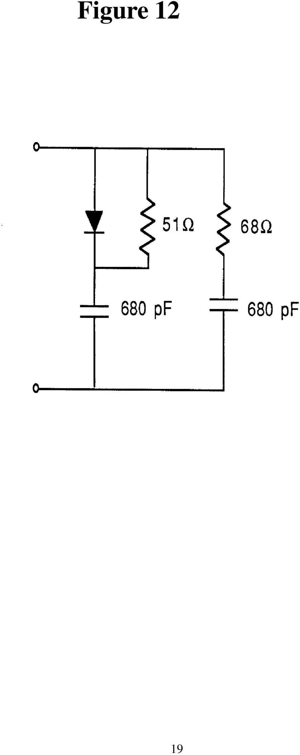
15 simultaneous maximum voltage and current is eliminated. The net result is much lower peak stress and switching loss. Voltage waveforms for two different values of C s are shown. In this example I o = 10 A and E o = 300 V. As C s is made larger the peak power and the switching loss will be lower. However, larger C s means greater loss in R s when the switch turns on and C s is discharged through R s and the switch. Again we see the tradeoff between snubber efficacy and loss. Depending on the size of C s the switch voltage may reach E o before, at the same time, or after the switch current reaches zero. The case where E = E o at the instant that I = 0 is defined as a normal snubber and C s = C [2] n, where : Where t s is the fall time of the switch current (see figure 9). For the example given in figure 9, C n = nf. The relationships between C n, switching loss, peak switch stress, snubber loss and total loss are shown in figure 10. Snubber size is shown relative to C n. When even a small snubber is used (C s < C n ) the switching loss drops quickly. As C s is made larger however, the improvement in switch loss decreases. For example, for C s = C n, the switch loss is down to 16%. Making C s larger will reduce the switching loss only a small amount but will increase the snubber loss substantially. There is in fact a broad minimum loss around C s = 0.45 C n, where the total loss is reduced to 53% of what it would have been without the snubber. It is important to remember that C p is part of C s and that the actual value for C s =.45 C n - C p. For C s /C n = 2 the total loss is equal to what it would have been if no snubber were used, however the switching load line will have very low stress. In those cases where the primary concern is to reduce the total switching loss, the value for C s is usually set to.5 Cn. In this case R s is selected to allow the voltage on C s to decay to a small value during the minimum switch on time (t on,min ). The capacitor voltage decay is a simple RC exponential and in two time constants (τ = R s C s ) will be down to 0.14 E o. This is usually sufficient. The value of R s is then: When L p is significant there will be voltage overshoot during turn-off. If E 1 must be controlled then different values for C s may be necessary and a compromise made. Figure 11 gives a comparison between the RC snubber developed earlier and an RCD snubber using the same component values (R s = 51W and C s = 680 pf). Note that the loss will be lower but the peak voltage is higher for the RCD snubber. This is typical. For similar total loss, C s can be larger in the RCD snubber which will reduce E 1. Increasing C s to 1.2 nf reduces E 1 to 424 V. C s could be increased further but for the same total loss, E 1 will still be higher in the RCD snubber. Combined snubber: When it is important to minimize both the loss in the switch and E 1 15

16 Figure 10 16

17 Figure 11 17

18 a combination snubber, using both RC and RCD, can produce very good results with low losses. An example of such a combination is given in figure 12 and the resulting waveform is compared to the previous RC snubber, using the same circuit conditions, in figure 13. Component selection and layout The components in snubbers can be very highly stressed and must therefore be selected with some care. Layout and inductance One of the primary reasons for using snubbers is the presence of parasitic inductances (L p ) in the circuit which generate voltage spikes and ringing when excited by the switching action. Larger parasitic inductance means larger snubber components and more dissipation. Before actually designing the snubber, it is important to minimize the circuit parasitic inductances and careful circuit layout is the key. As power levels rise this becomes progressively more important because of the increasing di/dt. Figure 14A illustrates a typical inverter pole or converter half-bridge. The bus which connects the source (V dc ) to the + and - ends of the pole will have some inherent inductance, both in the bus structure and in the energy storage capacitors (C 1, ESL). The effect of L p can be greatly reduced by placing smaller, low ESL, capacitors as close as possible to the switches as shown by C 2. One possibility is to use CDE snubber capacitor modules which connect directly to the IGBT module as shown in figure 15. These modules are available as either a simple capacitor or they may include one or more snubber diodes to implement an RCD snubber. In some cases the addition of C 2 by itself may not be a complete answer because the bus voltage may ring due to the resonance of Lp, C 1 and C 2. An alternative is to use an RCD snubber as a clamp as shown in figure 14B. The average voltage across C 2 will be equal to the bus voltage. At turn-off the voltage across C 2 will rise as it limits the peak switch voltage but later in the cycle the voltage is reset to the bus voltage through R s. R s also damps the bus voltage ringing. An additional advantage of this approach is that L p acts as a turn-on snubber, reducing turn-on switching loss. Because of the very large di/dt s which are common in snubbers, small amounts of parasitic inductance within the snubber can interfere with snubber action leading to higher than expected peak voltages. Parasitic inductance comes from two sources: intrinsic to the components due to physical size and lead configuration and from the layout. Component inductance can be minimized by the choice of package (radial versus axial for example) and can be further reduced by using several smaller devices in parallel. Paralleling is particularly useful in high power snubbers because in addition to allowing lower inductance configurations, it can improve the surface area-volume ratio allowing better cooling and higher rms currents. The primary source of layout inductance is the connection from the snubber components to the switch. The snubber components should be placed as close as possible to the switch terminals. The components should be arranged so that the current 18
 in the circuit which generate voltage spikes and ringing when excited by the")
19 Figure 12 19
20 Figure 13 20

21 Figure 14 21
22 loop formed by the snubber has a small an area (low inductance!) as possible. The CDE snubber modules shown in figure 15 are a very good example. With these modules, the snubber is connected directly across the switch terminals with low inductance strap leads. Capacitor selection: Snubber capacitors are subjected to high peak and rms currents and high dv/dt. An example of the turn-on and turn-off current spikes in a typical RCD snubber capacitor is given in figure 16. The pulses have high peak and rms amplitudes. CDE has several types of capacitors which are particularly well suited to snubber applications. Table 1 shows the various types and characteristics of capacitors intended for snubber applications. Table 1 Cornell Dubilier Capacitors for Snubber Applications STYLE PACKAGE DIELECTRIC ELECTRODE VOLTS RANGE CAP RANGE dv/dt Irms CD16 CDV16 CDV19 CD30 CDV30 Dipped with radial leads Mica Foil VDC ,000 pf >10,000 V/µs Up to 9 A WPP Wrap & Fill axial leads Polypropylene Foil VDC µf ,000 V/µs Up to 10 A DPF DPP Wrap & Fill axial leads Polypropylene Foil VDC µf ,000 V/µs Up to 10 A SCD Box type, direct mount to IGBT Polypropylene Double Metallized VDC µf V/µs Up to 50 A Wrap & Fill axial leads Polypropylene Double Metallized VDC µf V/µs Up to 25 A Wrap & Fill axial leads Polypropylene Hybridmetallized PP/ Foil VDC µf V/µs Up to 25 A Resistor selection: As pointed out earlier, it is important that R s, in an RC snubber, have low self inductance. Inductance in R s will increase the peak voltage (E 1 ) and tend to defeat the purpose of the snubber. Low inductance is also desirable for R s in an RCD snubber but is not as critical since the effect of a small amount of inductance is to slightly increase the reset time of C s and reduce the peak current somewhat in the switch at turn-on. The normal choice for Rs is usually carbon composition or metal film. For higher power levels low inductance wire wound resistors, such as the Dale Electronics NH types, can be used with some care to verify the actual residual inductance and its effect on the snubber action. Again, it is in the RC snubbers that parasitic inductance is most critical. 22
23 Figure 15 23
24 Figure 16 24
25 Diode selection: The diode in an RCD snubber has to be rated for at least the peak voltage which appears on C s. In general the average current in the diode is relatively small but the peak currents are substantial. The peak current should be the basis for selecting the diode. The diode reverse recovery time (t rr ) can effect the snubber action and fast or ultra-fast diodes with t rr < 100 ns are normally used. The performance of the diode should be verified in the circuit to be sure the snubber is performing as expected. As the voltage rating of the diode is increased and faster recovery diodes are selected, the forward recovery time (t fr ) may become a consideration. This is because the initial voltage drop across the diode, in the forward direction, can be much higher than the steady state conduction value for several hundred nsec. This problem is exacerbated by the very high di/dt of typical snubber current waveforms. By the time the diode is fully turned on, the snubber current pulse may be long finished. It may be necessary to try several different device types in the actual circuit to get satisfactory performance. Snubbers for IGBT inverters IGBTs are increasingly the switch of choice for inverters used in power electronics applications. IGBTs are replacing MOSFETs in many high voltage, hard switching applications since they have lower conduction losses and smaller die area for the same output power. The smaller die size translates to lower cost and smaller input capacitance. Most IGBT modules are used in hard switching applications of up to 20 KHz. Beyond that, switching losses in the IGBT become very significant. Switching such high currents in a short time gives rise to voltage transients that could exceed the rating of the IGBT especially if the bus voltage is close to the IGBT s voltage rating. The magnitude of the voltage transient is given by: where: Ls is the DC loop inductance di/dt is the rate of change of current with time Design engineers are encouraged to minimize the DC loop inductance. The use of laminated bus bars and improving circuit layout are ways of significantly reducing bus inductance; yet parasitic inductance will still be present. Snubbers are therefore needed to protect the switch from transients resulting from current changing in the parasitic inductance. In addition to providing protection from overvoltage, snubbers can be employed to: Limit di/dt or dv/dt Shape the load line to keep it within the safe operating area (SOA) Transfer power dissipation from the switch to a resistor Reduce total switching losses Reduce voltage and current ringing 25
26 There are three basic types of snubbers circuits used in IGBT applications. The type used will depend largely on the power level, switching frequency, and circuit layout. Figure 18 shows these snubber circuits and how they are applied to a half bridge rectifier. The de-coupling is the simplest of the three types. It is essentially a low inductance capacitor mounted across the bus, from C to E on a dual IGBT module, or from P to N on a six pack. The de-coupling is effective in reducing transients by providing a low inductance path during switching operation. Decoupling caps are typically used in low to medium current applications. In higher current applications, oscillations between the source and the de-coupling capacitor will produce ripple current that may cause the capacitor to fail. Cornell Dubilier offers 940, 941, and SCD (Direct mount) capacitors for de-coupling applications. The 940 series capacitors are axial leaded and can be mounted onto a PCB while style SCD caps are mounted directly to the IGBT module. Direct mount types have lower inducatance due to the flat, radial lead geometry. They are easy to install using the IGBT s own screws. Direct mount capacitors are rated for higher current because heavy copper lugs are connected directly to the capacitor element. The value of the capacitance needed for a de-coupling application depends on the stray inductance, maximum switching current, allowable peak voltage and dc bus voltage. The Snubber capacitance needed can be approximated from the following: 16 The difficulty in applying this formula is that bus inductance is often difficult to determine. Pages 10 through 12 of this application note provide a couple of methods for determining L. A good rule of thumb is to use 1 µf per 100 A of IGBT if inducatance cannot be determined directly. RCD snubbers are typically used in medium to high current applications. Direct mount snubbers containing hyperfast, soft recovery diodes are available from Cornell Dubilier. Style SCM may be used to protect dual IGBT modules by connecting them across the C and E terminals of the IGBT. See figure 18B. This snubber operates on the same principles as the de-coulping capacitor, but only during turn-off switching. As the IGBT turns off, energy trapped in the loop inductance is transferred to the capacitor. The diode blocks oscillations and the excess charge on the capacitor is dissipated through the external resistor. In higher current applications where the inverter is made of two single IGBT modules, P type and N type SCM snubbers may be applied to clamp the inverter voltage as shown in figure 18C. Dual IGBT modules may also be protected using an SCC style clamp module as shown in figure 18D. At turn off, the snubber diode is forward biased and the snubber is activated. The energy trapped in the stray inductance is absorbed by the snubber capacitor. During turn-on the snubber caps that were fully charged to bus voltage have a discharge path through the forward bias free-wheel diode, the IGBT, and the snubber resistor. This reduces the reverse recovery voltage transient. 26
27 Figure 18 a b c d 27
28 As the need for high power snubbers continues to increase, so does the need for information regarding appropriate component selection. This paper discussed the major types of snubbers, their application and methods for determining snubber component values. Use of these methods should lead to good component choice and ultimately good snubber design. References [1] William McMurray, OPTIMUM SNUBBERS FOR POWER SEMICONDUCTORS, IEEE IAS transactions, Vol. IA-8, No. 5, Sept/Oct 1972, pp [2] William McMurray, SELECTION OF SNUBBERS AND CLAMPS TO OPTIMIZE THE DESIGN OF TRANSISTOR SWITCHING CONVERTERS, IEEE IAS transactions, Vol. IA-16, No. 4, July/ August 1980, pp [3] Motto, E., EVALUATING THE DYNAMIC PERFORMANCE OF HIGH CURRENT IGBT MOD- ULES [4] Kurnia, Stielau, Venkataramanan and Divan, LOSS MECHANISMS IN IGBT S UNDER ZERO VOLTAGE SWITCHING, IEEE APEC 92 proceedings, pp [5] Wang, Lee, Hua and Borojevic, A COMPARATIVE STUDY OF SWITCHING LOSSES OF IGBT S UNDER HARD-SWITCHING, ZERO-VOLTAGE-SWITCHING AND ZERO-CURRENT-SWITCH- ING, IEEE PESC 94 proceedings, pp [6] Johansen, Jenset and Rogne, CHARACTERIZATION OF HIGH POWER IGBT S WITH SINEWAVE CURRENT, IEEE TRANSACTIONS ON INDUSTRY APPLICATIONS, VOL. 30, No. 5, September/October 1994, pp [7] Udeland, T., SWITCHING STRESS REDUCTION IN POWER TRNSISTOR CONVERTERS, IEEE IAS annual meeting proceedings, 1976, pp [8] Domb, M., NONDISSIPATIVE TURN-OFF SNUBBER ALLEVIATES SWITCHING POWER DISSIPATION, SECOND-BREAKDOWN STRESS AND V CE OVERSHOOT, IEEE PESC proceedings, 1982, pp [9] Zach, Kaiser, Kolar and Haselsteiner, NEW LOSSLES TURN-ON AND TURN-OFF (SNUBBER) NETWORKS FOR INVERTERS, INCLUDING CIRCUITS FOR BLOCKING VOLTAGE LIMITA- TION, IEEE TRANSACTIONS ON POWER ELECTRONICS, VOL. PE-1, NO. 2, April 1986, pp
29 [10] Bendien, Van Der Broeck and Fregien, RECOVERY CIRCUIT FOR SNUBBER ENERGY IN POWER ELECTRONIC APPLICATIONS WITH HIGH SWITCHING FREQUENCIES, IEEE TRANSACTIONS ON POWER ELECTRONICS, VOL. 3, NO. 1, January 1988, pp [11]Simonelli, and Torrey, AN ALTERNATIVE BUS CLAMP FOR RESONANT DC-LINK CON- VERTERS, IEEE TRANSACTIONS ON POWER ELECTRONICS, VOL. 9, NO. 1, January 1994, pp [12] Finney, Williams and Green, RCD SNUBBER REVISITED, IEEE TRANSACTIONS ON IN- DUSTRY APPLICATIONS, VOL. 32, NO. 1, January 1996, pp [13] McMurray, W., EFFICIENT SNUBBERS FOR VOLTAGE-SOURCE INVERTERS, IEEE PESC 85 proceedings, 1985, pp [14]Swanepoel and van Wyk, ANALYSIS AND OPTIMIZATION OF REGENERATIVE LINEAR SNUBBERS APPLIED TO SWITCHES WITH VOLTAGE AND CURRENT TAILS, IEEE TRANS- ACTIONS ON POWER ELECTRONICS, VOL. 9, N0. 4, July 1994, pp [15] Pearson and Sen, DESIGNING OPTIMUM SNUBBER CIRCUITS FOR THE TRANSISTOR BRIDGE CONFIGURATION, POWERCON 9 proceedings, 1982, pp. D-2-1 through D-2-11 [16] Zhang, Sobhani and Chokhawala, SNUBBER CONSIDERATIONS FOR IGBT APPLICA- TIONS, INTERNATIONAL RECTIFIER DESIGNER S MANUAL, IGBT-3, TPAP-5, 1995, pp. E135-E
High Performance ZVS Buck Regulator Removes Barriers To Increased Power Throughput In Wide Input Range Point-Of-Load Applications
 White paper High Performance ZVS Buck Regulator Removes Barriers To Increased Power Throughput In Wide Input Range Point-Of-Load Applications Written by: C. R. Swartz Principal Engineer, Picor Semiconductor
Application Note AN- 1095
 Application Note AN- 1095 Design of the Inverter Output Filter for Motor Drives with IRAMS Power Modules Cesare Bocchiola Table of Contents Page Section 1: Introduction...2 Section 2 : Output Filter Design
Inrush Current. Although the concepts stated are universal, this application note was written specifically for Interpoint products.
 INTERPOINT Although the concepts stated are universal, this application note was written specifically for Interpoint products. In today s applications, high surge currents coming from the dc bus are a
Design and Applications of HCPL-3020 and HCPL-0302 Gate Drive Optocouplers
 Design and Applications of HCPL-00 and HCPL-00 Gate Drive Optocouplers Application Note 00 Introduction The HCPL-00 (DIP-) and HCPL-00 (SO-) consist of GaAsP LED optically coupled to an integrated circuit
UNDERSTANDING AND CONTROLLING COMMON-MODE EMISSIONS IN HIGH-POWER ELECTRONICS
 Page 1 UNDERSTANDING AND CONTROLLING COMMON-MODE EMISSIONS IN HIGH-POWER ELECTRONICS By Henry Ott Consultants Livingston, NJ 07039 (973) 992-1793 www.hottconsultants.com [email protected] Page 2 THE BASIC
Chapter 4. LLC Resonant Converter
 Chapter 4 LLC Resonant Converter 4.1 Introduction In previous chapters, the trends and technical challenges for front end DC/DC converter were discussed. High power density, high efficiency and high power
Design of an Auxiliary Power Distribution Network for an Electric Vehicle
 Design of an Auxiliary Power Distribution Network for an Electric Vehicle William Chen, Simon Round and Richard Duke Department of Electrical & Computer Engineering University of Canterbury, Christchurch,
Designers Series XII. Switching Power Magazine. Copyright 2005
 Designers Series XII n this issue, and previous issues of SPM, we cover the latest technologies in exotic high-density power. Most power supplies in the commercial world, however, are built with the bread-and-butter
Application Note AN-1070
 Application Note AN-1070 Class D Audio Amplifier Performance Relationship to MOSFET Parameters By Jorge Cerezo, International Rectifier Table of Contents Page Abstract... 2 Introduction... 2 Key MOSFET
FILM CAPACITORS FOR ELECTRONIC LIGHTING
 1. Introduction: FILM CAPACITORS FOR ELECTRONIC LIGHTING G. Schabbach, Dr. K. Weigel, Dr. G. Zimmermann EPCOS AG Fluorescent lamps have emerged as the preferred light source for industrial and domestic
Input and Output Capacitor Selection
 Application Report SLTA055 FEBRUARY 2006 Input and Output Capacitor Selection Jason Arrigo... PMP Plug-In Power ABSTRACT When designing with switching regulators, application requirements determine how
Philosophy of Topology and Components Selection for Cost and Performance in Automotive Converters.
 Philosophy of Topology and Components Selection for Cost and Performance in Automotive Converters. Alexander Isurin ( [email protected] ) Alexander Cook ([email protected] ) Vanner inc. USA Abstract- This
Eliminating Parasitic Oscillation between Parallel MOSFETs
 Eliminating Parasitic Oscillation between Parallel MOSFETs Based in part on a paper presented at Power Electronics Technology 2003 conference titled Issues with Paralleling MOSFETs and IGBTs by Jonathan
Power Supplies. 1.0 Power Supply Basics. www.learnabout-electronics.org. Module
 Module 1 www.learnabout-electronics.org Power Supplies 1.0 Power Supply Basics What you ll learn in Module 1 Section 1.0 Power Supply Basics. Basic functions of a power supply. Safety aspects of working
Line Reactors and AC Drives
 Line Reactors and AC Drives Rockwell Automation Mequon Wisconsin Quite often, line and load reactors are installed on AC drives without a solid understanding of why or what the positive and negative consequences
Introduction to Power Supplies
 Introduction to Power Supplies INTRODUCTION Virtually every piece of electronic equipment e g computers and their peripherals calculators TV and hi-fi equipment and instruments is powered from a DC power
Rectifier circuits & DC power supplies
 Rectifier circuits & DC power supplies Goal: Generate the DC voltages needed for most electronics starting with the AC power that comes through the power line? 120 V RMS f = 60 Hz T = 1667 ms) = )sin How
Drive circuit basics + V. τ e. Industrial Circuits Application Note. Winding resistance and inductance
 ndustrial Circuits Application Note Drive circuit basics For a given size of a stepper motor, a limited space is available for the windings. n the process of optimizing a stepper motor drive system, an
DRIVE CIRCUITS FOR POWER MOSFETs AND IGBTs
 DRIVE CIRCUITS FOR POWER MOSFETs AND IGBTs by B. Maurice, L. Wuidart 1. INTRODUCTION Unlike the bipolar transistor, which is current driven, Power MOSFETs, with their insulated gates, are voltage driven.
New High Current MOSFET Module Offers 177 µω R DS(on)
") ew High Current Offers 177 µω R D(on) By William C. Kephart, Eric R. Motto Application Engineering owerex Incorporated Abstract This paper describes a new family of high current modules optimized for industrial
ew High Current Offers 177 µω R D(on) By William C. Kephart, Eric R. Motto Application Engineering owerex Incorporated Abstract This paper describes a new family of high current modules optimized for industrial
O p t i m u m M O S F E T S e l e c t i o n f o r S y n c h r o n o u s R e c t i f i c a t i o n
 V2.4. May 2012 O p t i m u m M O S F E T S e l e c t i o n f o r S y n c h r o n o u s R e c t i f i c a t i o n IFAT PMM APS SE DS Mößlacher Christian Guillemant Olivier Edition 2011-02-02 Published by
Influence of Short Circuit conditions on IGBT Short circuit current in motor drives
 Influence of Short Circuit conditions on IGBT Short circuit current in motor drives Vijay Bolloju, IGBT Applications Manager, International Rectifier, El Segundo, CA USA Jun Yang IGBT Applications Engineer,
IGBT Peak Voltage Measurement and Snubber Capacitor Specification
 Application Note AN-7006 Revision: Issue Date: Prepared by: 00 2008-03-17 Joachim Lamp Key Words: module, snubber capacitor, peak voltage Peak Voltage Measurement and Snubber Capacitor Specification General...
Diode Applications. by Kenneth A. Kuhn Sept. 1, 2008. This note illustrates some common applications of diodes.
 by Kenneth A. Kuhn Sept. 1, 2008 This note illustrates some common applications of diodes. Power supply applications A common application for diodes is converting AC to DC. Although half-wave rectification
AN ISOLATED GATE DRIVE FOR POWER MOSFETs AND IGBTs
 APPLICATION NOTE AN ISOLATED GATE DRIVE FOR POWER MOSFETs AND IGBTs by J.M. Bourgeois ABSTRACT Power MOSFET and IGBT gate drives often face isolation and high voltage constraints. The gate drive described
Understanding Power Impedance Supply for Optimum Decoupling
 Introduction Noise in power supplies is not only caused by the power supply itself, but also the load s interaction with the power supply (i.e. dynamic loads, switching, etc.). To lower load induced noise,
Transistor Amplifiers
 Physics 3330 Experiment #7 Fall 1999 Transistor Amplifiers Purpose The aim of this experiment is to develop a bipolar transistor amplifier with a voltage gain of minus 25. The amplifier must accept input
The leakage inductance of the power transformer
 Nondissipative lamping Benefits - onverters Even if small, a transformer s leakage inductance reduces the efficiency of some isolated dc-dc converter topologies However, the technique of lossless voltage
The full wave rectifier consists of two diodes and a resister as shown in Figure
 The Full-Wave Rectifier The full wave rectifier consists of two diodes and a resister as shown in Figure The transformer has a centre-tapped secondary winding. This secondary winding has a lead attached
RC NETWORKS SALES GUIDE
 SALES GUIDE INTRODUCTION TO Recent developments in electronic equipment have shown the following trends: Increasing demands for numerical control machines, robotics and technically advanced appliances
ULRASONIC GENERATOR POWER CIRCUITRY. Will it fit on PC board
 ULRASONIC GENERATOR POWER CIRCUITRY Will it fit on PC board MAJOR COMPONENTS HIGH POWER FACTOR RECTIFIER RECTIFIES POWER LINE RAIL SUPPLY SETS VOLTAGE AMPLITUDE INVERTER INVERTS RAIL VOLTAGE FILTER FILTERS
TOPOLOGIES FOR SWITCHED MODE POWER SUPPLIES
 TOPOLOGIES FOR SWITCHED MODE POWER SUPPLIES by L. Wuidart I INTRODUCTION This paper presents an overview of the most important DC-DC converter topologies. The main object is to guide the designer in selecting
Novel Loaded-Resonant Converter & Application of DC-to-DC Energy Conversions systems
 International Refereed Journal of Engineering and Science (IRJES) ISSN (Online) 2319-183X, (Print) 2319-1821 Volume 2, Issue 11 (November 2013), PP.50-57 Novel Loaded-Resonant Converter & Application of
Variable Frequency Drives - a Comparison of VSI versus LCI Systems
 Variable Frequency Drives - a Comparison of VSI versus LCI Systems Introduction TMEIC is a leader in the innovative design and manufacture of large ac variable f requency drive systems. TMEIC has been
I. INTRODUCTION II. MOSFET FAILURE MODES IN ZVS OPERATION
 MOSFET Failure Modes in the Zero-Voltage-Switched Full-Bridge Switching Mode Power Supply Applications Alexander Fiel and Thomas Wu International Rectifier Applications Department El Segundo, CA 9045,
A Zero-Voltage Switching Two-Inductor Boost Converter With an Auxiliary Transformer
 A Zero-Voltage Switching Two-Inductor Boost Converter With an Auxiliary Transformer Quan Li and Peter Wolfs Central Queensland University Rockhampton Mail Center, QLD 47, Australia Abstract-The two-inductor
Bridgeless PFC Implementation Using One Cycle Control Technique
 Bridgeless PFC Implementation Using One Cycle Control Technique Bing Lu Center for Power Electronics Systems Virginia Polytechnic Institute and State University 674 Whittemore Hall Blacksburg, VA 24061
Understanding Diode Reverse Recovery and its Effect on Switching Losses
 Understanding Diode Reverse Recovery and its Effect on Switching Losses Peter Haaf, Senior Field Applications Engineer, and Jon Harper, Market Development Manager, Fairchild Semiconductor Europe Abstract
Transmission Line Terminations It s The End That Counts!
 In previous articles 1 I have pointed out that signals propagating down a trace reflect off the far end and travel back toward the source. These reflections can cause noise, and therefore signal integrity
AN11160. Designing RC snubbers
 AN60 Rev. 25 April 202 Application note Document information Info Keywords Abstract Content RC snubber, commutation, reverse recovery, leakage inductance, parasitic capacitance, RLC circuit and damping,
Application Guide Film Capacitors
 Capacitance Change vs. Temperature Insulation Resistance vs. Temperature Polyester Typical Characteristics at 1 khz % Capacitance Change % Capacitance Change Polypropylene Typical Characteristics at 1
MEETING TRANSIENT SPECIFICATIONS FOR ELECTRICAL SYSTEMS IN MILITARY VEHICLES
 MEETING TRANSIENT SPECIFICATIONS FOR ELECTRICAL SYSTEMS IN MILITARY VEHICLES By Arthur Jordan Sr. Applications Engineer, Vicor Electrical systems in military vehicles are normally required to meet stringent
DIODE CIRCUITS LABORATORY. Fig. 8.1a Fig 8.1b
 DIODE CIRCUITS LABORATORY A solid state diode consists of a junction of either dissimilar semiconductors (pn junction diode) or a metal and a semiconductor (Schottky barrier diode). Regardless of the type,
Output Ripple and Noise Measurement Methods for Ericsson Power Modules
 Output Ripple and Noise Measurement Methods for Ericsson Power Modules Design Note 022 Ericsson Power Modules Ripple and Noise Abstract There is no industry-wide standard for measuring output ripple and
Harmonics and Noise in Photovoltaic (PV) Inverter and the Mitigation Strategies
 Inverter and the Mitigation Strategies") Soonwook Hong, Ph. D. Michael Zuercher Martinson Harmonics and Noise in Photovoltaic (PV) Inverter and the Mitigation Strategies 1. Introduction PV inverters use semiconductor devices to transform the
Soonwook Hong, Ph. D. Michael Zuercher Martinson Harmonics and Noise in Photovoltaic (PV) Inverter and the Mitigation Strategies 1. Introduction PV inverters use semiconductor devices to transform the
POWER LINE FILTERS FOR SWITCHING POWER SUPPLIES
 POWER INE FITERS FOR SWITCHING POWER SUPPIES ing. Eugen COCA *, prof. dr. ing. Dimitrie AEXA ** * EECTRICA SA - SD SUCEAVA - ROMANIA ** U.T. Gh. Asachi IASI - ROMANIA * SEM0kV - PRAM str. Stefan cel Mare,
Soft-Switching in DC-DC Converters: Principles, Practical Topologies, Design Techniques, Latest Developments
 Soft-Switching in D-D onverters: Principles, Practical Topologies, Design Techniques, Latest Developments Raja Ayyanar Arizona State University Ned Mohan University of Minnesota Eric Persson International
Two-Switch Forward Converter: Operation, FOM, and MOSFET Selection Guide
 VISHAY SILICONIX www.vishay.com MOSFETs by Philip Zuk and Sanjay Havanur The two-switch forward converter is a widely used topology and considered to be one of the most reliable converters ever. Its benefits
ENGR-4300 Electronic Instrumentation Quiz 4 Spring 2011 Name Section
 ENGR-4300 Electronic Instrumentation Quiz 4 Spring 2011 Name Section Question I (20 points) Question II (20 points) Question III (20 points) Question IV (20 points) Question V (20 points) Total (100 points)
Bourns Resistive Products
 Bourns Resistive Products Diverse Requirements Drive Innovations to Pulse Resistors Introduction Countless circuits depend on the protection provided by one of the most fundamental types of passive components:
What Is Regeneration?
 What Is Regeneration? Braking / Regeneration Manual Regeneration Overview Revision 1.0 When the rotor of an induction motor turns slower than the speed set by the applied frequency, the motor is transforming
Bipolar Transistor Amplifiers
 Physics 3330 Experiment #7 Fall 2005 Bipolar Transistor Amplifiers Purpose The aim of this experiment is to construct a bipolar transistor amplifier with a voltage gain of minus 25. The amplifier must
Application Note 9020. IGBT Basic II CONTENTS. April, 2002. By K.J Um. Section I. Gate drive considerations
 B. R G a. Effect on turn-on Application Note 9020 April, 2002 IGBT Basic II By K.J Um CONTENTS Section I. Gate drive considerations 1. Introductions 2. Gate Drive Considerations 3. IGBT switching waveforms
Lecture - 4 Diode Rectifier Circuits
 Basic Electronics (Module 1 Semiconductor Diodes) Dr. Chitralekha Mahanta Department of Electronics and Communication Engineering Indian Institute of Technology, Guwahati Lecture - 4 Diode Rectifier Circuits
H a r d C o m m u t a t i o n o f P o w e r M O S F E T
 H a r d C o m m u t a t i o n o f P o w e r M O S F E T O p t i M O S TM F D 2 0 0 V / 2 5 0 V IFAT PMM APS SE DC Alan Huang Edition 2014-03-12 Published by Infineon Technologies Austria AG 9500 Villach,
Design and Simulation of Soft Switched Converter Fed DC Servo Drive
 International Journal of Soft Computing and Engineering (IJSCE) ISSN: 2231-237, Volume-1, Issue-5, November 211 Design and Simulation of Soft Switched Converter Fed DC Servo Drive Bal Mukund Sharma, A.
Chapter 3. Diodes and Applications. Introduction [5], [6]
![Chapter 3. Diodes and Applications. Introduction [5], [6]](/thumbs/40/21801962.jpg "Chapter 3. Diodes and Applications. Introduction [5], [6]") Chapter 3 Diodes and Applications Introduction [5], [6] Diode is the most basic of semiconductor device. It should be noted that the term of diode refers to the basic p-n junction diode. All other diode
Chapter 3 Diodes and Applications Introduction [5], [6] Diode is the most basic of semiconductor device. It should be noted that the term of diode refers to the basic p-n junction diode. All other diode
Transformerless UPS systems and the 9900 By: John Steele, EIT Engineering Manager
 Transformerless UPS systems and the 9900 By: John Steele, EIT Engineering Manager Introduction There is a growing trend in the UPS industry to create a highly efficient, more lightweight and smaller UPS
Impedance Matching and Matching Networks. Valentin Todorow, December, 2009
 Impedance Matching and Matching Networks Valentin Todorow, December, 2009 RF for Plasma Processing - Definition of RF What is RF? The IEEE Standard Dictionary of Electrical and Electronics Terms defines
Common Mode Filter Inductor Analysis
 Document 2-1 Common Mode Filter Inductor Analysis Abstract Noise limits set by regulatory agencies make solutions to common mode EMI a necessary consideration in the manufacture and use of electronic equipment.
LOW COST MOTOR PROTECTION FILTERS FOR PWM DRIVE APPLICATIONS STOPS MOTOR DAMAGE
 LOW COST MOTOR PROTECTION FILTERS FOR PWM DRIVE APPLICATIONS STOPS MOTOR DAMAGE Karl M. Hink, Executive Vice President Originally presented at the Power Quality 99 Conference ABSTRACT Motor protection
Considering the effects of UPS operation with leading power factor loads
 Considering the effects of UPS operation with leading power factor loads Over the past five years, a new generation of data processing and communications equipment has become prevalent in modern data centers
High Voltage Power Supplies for Analytical Instrumentation
 ABSTRACT High Voltage Power Supplies for Analytical Instrumentation by Cliff Scapellati Power supply requirements for Analytical Instrumentation are as varied as the applications themselves. Power supply
Application Note, Rev.1.0, September 2008 TLE8366. Application Information. Automotive Power
 Application Note, Rev.1.0, September 2008 TLE8366 Automotive Power Table of Contents 1 Abstract...3 2 Introduction...3 3 Dimensioning the Output and Input Filter...4 3.1 Theory...4 3.2 Output Filter Capacitor(s)
Keywords: input noise, output noise, step down converters, buck converters, MAX1653EVKit
 Maxim > Design Support > Technical Documents > Tutorials > Power-Supply Circuits > APP 986 Keywords: input noise, output noise, step down converters, buck converters, MAX1653EVKit TUTORIAL 986 Input and
IEC 1000-4-2 ESD Immunity and Transient Current Capability for the SP72X Series Protection Arrays
 IEC 00-4-2 ESD Immunity and Transient Current Capability for the SP72X Series Protection Arrays Application Note July 1999 AN9612.2 Author: Wayne Austin The SP720, SP721, SP723, and SP724 are protection
FPAB20BH60B PFC SPM 3 Series for Single-Phase Boost PFC
 FPAB20BH60B PFC SPM 3 Series for Single-Phase Boost PFC Features UL Certified No. E209204 (UL1557) 600 V - 20 A Single-Phase Boost PFC with Integral Gate Driver and Protection Very Low Thermal Resistance
GENERAL POWER SYSTEM WIRING PRACTICES APPLIED TO TECNADYNE DC BRUSHLESS MOTORS
 1/5/2006 Page 1 of 6 GENERAL POWER SYSTEM WIRING PRACTICES APPLIED TO TECNADYNE DC BRUSHLESS MOTORS 1. Introduction The purpose of this application note is to describe some common connection and filtering
High Intensify Interleaved Converter for Renewable Energy Resources
 High Intensify Interleaved Converter for Renewable Energy Resources K. Muthiah 1, S.Manivel 2, Gowthaman.N 3 1 PG Scholar, Jay Shriram Group of Institutions,Tirupur 2 Assistant Professor, Jay Shriram Group
AC Motor Drive. page 1
 AC Motor Drive Table of Contents AC Input, Diode Bridges... 3 AC Input, Power Factor Correction...4 AC Input, X/Y Capacitors... 5 BIAS Supply (off-line, flyback), Discretes... 6 BIAS Supply (off-line,
6.101 Final Project Report Class G Audio Amplifier
 6.101 Final Project Report Class G Audio Amplifier Mark Spatz 4/3/2014 1 1 Introduction For my final project, I designed and built a 150 Watt audio amplifier to replace the underpowered and unreliable
SUCCESS EPCOS Capacitors
 SUCCESS EPCOS Inc. Capacitors Group April, 2012 EV / HV / E-Mobility Battery charger system & Inverter On Board and Off Board Assembly Trend: Wireless Charging DC/DC Converter Filtering DC Link E-Mobility
UNDERSTANDING POWER FACTOR AND INPUT CURRENT HARMONICS IN SWITCHED MODE POWER SUPPLIES
 UNDERSTANDING POWER FACTOR AND INPUT CURRENT HARMONICS IN SWITCHED MODE POWER SUPPLIES WHITE PAPER: TW0062 36 Newburgh Road Hackettstown, NJ 07840 Feb 2009 Alan Gobbi About the Author Alan Gobbi Alan Gobbi
Step Response of RC Circuits
 Step Response of RC Circuits 1. OBJECTIVES...2 2. REFERENCE...2 3. CIRCUITS...2 4. COMPONENTS AND SPECIFICATIONS...3 QUANTITY...3 DESCRIPTION...3 COMMENTS...3 5. DISCUSSION...3 5.1 SOURCE RESISTANCE...3
DIRECT CURRENT GENERATORS
 DIRECT CURRENT GENERATORS Revision 12:50 14 Nov 05 INTRODUCTION A generator is a machine that converts mechanical energy into electrical energy by using the principle of magnetic induction. This principle
= V peak 2 = 0.707V peak
 BASIC ELECTRONICS - RECTIFICATION AND FILTERING PURPOSE Suppose that you wanted to build a simple DC electronic power supply, which operated off of an AC input (e.g., something you might plug into a standard
Application Note 58 Crystal Considerations with Dallas Real Time Clocks
 www.dalsemi.com Application Note 58 Crystal Considerations with Dallas Real Time Clocks Dallas Semiconductor offers a variety of real time clocks (RTCs). The majority of these are available either as integrated
Switch Mode Power Supply Topologies
 Switch Mode Power Supply Topologies The Buck Converter 2008 Microchip Technology Incorporated. All Rights Reserved. WebSeminar Title Slide 1 Welcome to this Web seminar on Switch Mode Power Supply Topologies.
Tamura Closed Loop Hall Effect Current Sensors
 Tamura Closed Loop Hall Effect Current Sensors AC, DC, & Complex Currents Galvanic Isolation Fast Response Wide Frequency Bandwidth Quality & Reliability RoHs Compliance Closed Loop Hall Effect Sensors
LABORATORY 10 TIME AVERAGES, RMS VALUES AND THE BRIDGE RECTIFIER. Bridge Rectifier
 LABORATORY 10 TIME AVERAGES, RMS VALUES AND THE BRIDGE RECTIFIER Full-wave Rectification: Bridge Rectifier For many electronic circuits, DC supply voltages are required but only AC voltages are available.
4. ACTIVE-CLAMP BOOST AS AN ISOLATED PFC FRONT-END CONVERTER
 4. ACTIVE-CLAMP BOOST AS AN ISOLATED PFC FRONT-END CONVERTER 4.1 Introduction This chapter continues the theme set by Chapter 3 - simplifying the standard two-stage front-end implementation to one that
Power MOSFET Tutorial
 Power MOSFET Tutorial Jonathan Dodge, P.E. Applications Engineering Manager Advanced Power Technology 405 S.W. Columbia Street Bend, OR 97702 Introduction Power MOSFETs are well known for superior switching
The Flyback Converter
 The Flyback Converter Lecture notes ECEN4517! Derivation of the flyback converter: a transformer-isolated version of the buck-boost converter! Typical waveforms, and derivation of M(D) = V/! Flyback transformer
Chapter 2 Application Requirements
 Chapter 2 Application Requirements The material presented in this script covers low voltage applications extending from battery operated portable electronics, through POL-converters (Point of Load), internet
AN-1012: Reverse Recovery Time (T RR ) of the Super Barrier Rectifier TM Applications Department, APD Semiconductor, San Jose CA
 of the Super Barrier Rectifier TM Applications Department, APD Semiconductor, San Jose CA") AN-1012: Reverse Recovery Time (T RR ) of the Super Barrier Rectifier TM Applications Department, APD Semiconductor, San Jose CA There are many elements to a Reverse Recovery Time (T RR ) waveform and
AN-1012: Reverse Recovery Time (T RR ) of the Super Barrier Rectifier TM Applications Department, APD Semiconductor, San Jose CA There are many elements to a Reverse Recovery Time (T RR ) waveform and
3-Phase Synchronous PWM Controller IC Provides an Integrated Solution for Intel VRM 9.0 Design Guidelines
 3-Phase Synchronous PWM Controller IC Provides an Integrated Solution for Intel VRM 9.0 Design Guidelines Odile Ronat International Rectifier The fundamental reason for the rapid change and growth in information
Joule Thief 3.0 Kit. June 2012, Rev 1 1 http://www.easternvoltageresearch.com Joule Thief 3.0
 Kit Instruction Manual Eastern Voltage Research, LLC June 2012, Rev 1 1 http://www.easternvoltageresearch.com HIGH BRIGHTNESS LED THIS KIT USES A 1W CREE, HIGH BRIGHTNESS LED. DO NOT STARE AT THIS (OR
Digital Energy ITI. Instrument Transformer Basic Technical Information and Application
 g Digital Energy ITI Instrument Transformer Basic Technical Information and Application Table of Contents DEFINITIONS AND FUNCTIONS CONSTRUCTION FEATURES MAGNETIC CIRCUITS RATING AND RATIO CURRENT TRANSFORMER
IGBT Protection in AC or BLDC Motor Drives by Toshio Takahashi
 International Rectifier 233 Kansas Street, El Segundo, CA 90245 USA IGBT Protection in AC or BLDC Motor Drives by Toshio Takahashi The new IR2137 IGBT Gate Driver IC integrates Ground Fault and Over-Current
Circuits with inductors and alternating currents. Chapter 20 #45, 46, 47, 49
 Circuits with inductors and alternating currents Chapter 20 #45, 46, 47, 49 RL circuits Ch. 20 (last section) Symbol for inductor looks like a spring. An inductor is a circuit element that has a large
Unit/Standard Number. High School Graduation Years 2010, 2011 and 2012
 1 Secondary Task List 100 SAFETY 101 Demonstrate an understanding of State and School safety regulations. 102 Practice safety techniques for electronics work. 103 Demonstrate an understanding of proper
Module 11: Conducted Emissions
 Module 11: Conducted Emissions 11.1 Overview The term conducted emissions refers to the mechanism that enables electromagnetic energy to be created in an electronic device and coupled to its AC power cord.
GS66516T Top-side cooled 650 V E-mode GaN transistor Preliminary Datasheet
 Features 650 V enhancement mode power switch Top-side cooled configuration R DS(on) = 25 mω I DS(max) = 60 A Ultra-low FOM Island Technology die Low inductance GaNPX package Easy gate drive requirements
A bidirectional DC-DC converter for renewable energy systems
 BULLETIN OF THE POLISH ACADEMY OF SCIENCES TECHNICAL SCIENCES Vol. 57, No. 4, 2009 A bidirectional DC-DC converter for renewable energy systems S. JALBRZYKOWSKI, and T. CITKO Faculty of Electrical Engineering,
Case Studies in On-Line Measurement of PD in Motors Fed by Voltage Source PWM Drives
 Case Studies in On-Line Measurement of PD in Motors Fed by Voltage Source PWM Drives G.C. Stone, I. Culbert, H.G. Sedding Qualitrol-Iris Power Mississauga, Ontario, Canada Abstract On-line partial discharge
Application Note AN-983
 Application Note AN-983 IGBT Characteristics Table of Contents 1. How the IGBT complements the power MOSFET... 2 Page 2. Silicon structure and equivalent circuit... 2 3. Conduction characteristics... 4
POWER SYSTEM HARMONICS. A Reference Guide to Causes, Effects and Corrective Measures AN ALLEN-BRADLEY SERIES OF ISSUES AND ANSWERS
 A Reference Guide to Causes, Effects and Corrective Measures AN ALLEN-BRADLEY SERIES OF ISSUES AND ANSWERS By: Robert G. Ellis, P. Eng., Rockwell Automation Medium Voltage Business CONTENTS INTRODUCTION...
Power MOSFET. IRF510PbF SiHF510-E3 IRF510 SiHF510. PARAMETER SYMBOL LIMIT UNIT Drain-Source Voltage V DS 100 V Gate-Source Voltage V GS ± 20
 Power MOSFET PRODUCT SUMMARY (V) 100 R DS(on) () = 0.54 Q g max. (nc) 8.3 Q gs (nc) 2.3 Q gd (nc) 3.8 Configuration Single D TO220AB G FEATURES Dynamic dv/dt rating Available Repetitive avalanche rated
Product Data Bulletin
 Product Data Bulletin Power System Harmonics Causes and Effects of Variable Frequency Drives Relative to the IEEE 519-1992 Standard Raleigh, NC, U.S.A. INTRODUCTION This document describes power system
Modeling and Analysis of DC Link Bus Capacitor and Inductor Heating Effect on AC Drives (Part I)
") 00-00-//$0.00 (c) IEEE IEEE Industry Application Society Annual Meeting New Orleans, Louisiana, October -, Modeling and Analysis of DC Link Bus Capacitor and Inductor Heating Effect on AC Drives (Part
00-00-//$0.00 (c) IEEE IEEE Industry Application Society Annual Meeting New Orleans, Louisiana, October -, Modeling and Analysis of DC Link Bus Capacitor and Inductor Heating Effect on AC Drives (Part