DIEGO TONINI MORPHOLOGY OF NIOBIUM FILMS SPUTTERED AT DIFFERENT TARGET SUBSTRATE ANGLE
|
|
|
- Beryl Baldwin
- 9 years ago
- Views:
Transcription
1 UNIVERSITÀ DEGLI STUDI DI PADOVA SCIENCE FACULTY MATERIAL SCIENCE DEGREE INFN LABORATORI NAZIONALI DI LEGNARO DIEGO TONINI MORPHOLOGY OF NIOBIUM FILMS SPUTTERED AT DIFFERENT TARGET SUBSTRATE ANGLE

2 2 QUESTIONS What is the effect of target substrate angle on the film properties? How the film morphology varies changing target substrate angle?

3 DEPOSITIONS MADE AT DIFFERENT TARGET SUBSTRATE ANGLE FILM MORPHOLOGY CRYSTAL STRUCTURE THICKNESS AFM IMAGING ELECTROCHEMICAL IMPEDANCE SPECTROSCOPY SUPERCONDUCTING PROPERTIES T C MEASURE RRR MAGNETO-OPTICAL X-RAY DIFFRACTION TEXTURE ANALYSIS

4 MULTI-ANGLE SAMPLE HOLDER 7 substrates coated in the same run Almost identical process conditions for each sample

5 DC MAGNETRON SPUTTERING LOWER T C AND RRR INCREASING TARGET SUBSTRATE ANGLE

6 PULSED MAGNETRON SPUTTERING BETTER PROPERTIES FOR PULSED CURRENT DEPOSITION THERE IS STILL THE SAME ANGLE DEPENDENCE OF T C AND RRR

7 DC MAGNETRON SPUTTERING WITH SUBSTRATE HEATING T RRR C (K) Substrate temperature kept at 600 C during process 1. Better properties 2. Less angle sensitivity deposition angle (degrees)

8 XRD SPECTRA OF FILM DEPOSITED AT DIFFERENT TARGET SUBSTRATE ANGLE Relative Intensity degrees Theta (degrees) 75 degrees 60 degrees 45 degrees 30 degrees
 75 degrees 60 degrees 45 degrees")
9 ESTIMATED GRAIN DIMENSION crystallite dimension (Angstrom) D = 0.9λ cos( θ ) (2θ ) deposition angle (degrees)

10 d 110 OF CRYSTAL PLANES 3,0 2 ( ) d sin = hkl θ nλ 2,8 2,6 2,4 d 110 (Angstrom) 2,2 2,0 1,8 1,6 1,4 1,2 1, deposition angle (degrees)

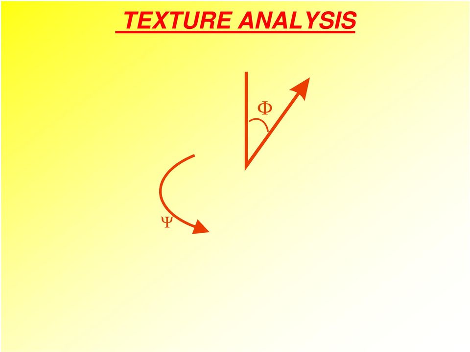
11 TEXTURE ANALYSIS
12 DC MAGNETRON SPUTTERING 0 gradi 15 gradi 30 gradi 45 gradi 60 gradi 75 gradi

13 PULSED MAGNETRON SPUTTERING 0 gradi 15 gradi 30 gradi 45 gradi 60 gradi 75 gradi

14 TEXTURE ANALYSIS DC VS PULSED MAGNETRON SPUTTERING 50 DC PULSED Φ max counts (degrees) deposition angle (degrees)

15 ATOMIC FORCE MICROSCOPY TOPOGRAPHIC IMAGES 15 gradi 30 gradi 45 gradi 60 gradi 75 gradi 90 gradi

16 ATOMIC FORCE MICROSCOPY DC MAGNETRON SPUTTERING roughness (nm) roughness (nm) deposition angle (degrees) deposition angle (degrees) Variable thickness Uniform thickness
 deposition angle (degrees) Variable thickness Uniform")
17 ATOMIC FORCE MICROSCOPY PULSED MAGNETRON SPUTTERING I campioni depositati in corrente pulsata sono sistematicamente più rugosi

18 ELECTROCHEMICAL IMPEDANCE SPECTROSCOPY V ( t) = V0 cos( ωt) I( t) = I 0 cos( ωt ϕ ) Z = V ( t) I( t) = Z 0 cos( ωt) cos( ωt ϕ) Z = Z 0e jϕ
 = Z 0 cos( ωt) cos( ωt ϕ) Z")
19 ELECTROCHEMICAL IMPEDANCE SPECTROSCOPY NYQUIST PLOT FLAT ELECTRODE: 6 ideally flat electrode porous electrode Real part of impedance represents R s at any frequency Im(Z) /arbitrary units 4 2 Immaginary part does not vary with frequency NYQUIST PLOT IS A VERTICAL LINE POROUS/ROUGH ELETRODE: Re(Z) / arbitrary units The apparent capacity C dl depends on frequency because the penetration length of electric field inside the pores raises when decreasing frequency. NYQUIST PLOT IS A 45 INCLINED LINE

20 ELECTROCHEMICAL IMPEDANCE SPECTROSCOPY DC MAGNETRON SPUTTERING VARIABLE FILM THICKNESS Up to 45 there is porous electrode behaviour Film deposited at higher angles are less thick so resistence is greaer

21 ELECTROCHEMICAL IMPEDANCE SPECTROSCOPY DC MAGNETRON SPUTTERING COMPARISON BETWEEN FILM WITH DIFFERENT THICKNESS AND FILM WITH CONSTANT THICKNESS Films with the same thickness have the same resistance There is a maximum in capacity at 60 target substrate angle
22 ELECTROCHEMICAL IMPEDANCE SPECTROSCOPY DC MAGNETRON SPUTTERING Films with the same thickness measures in passivaton condition Imposed potential to create a passivation layer on the film Oxide tichkness depends only on applied potential Oxide growth follows niobium film morphology Capacity shows the same angle dependence of non oxidized films
23 ELECTROCHEMICAL IMPEDANCE SPECTROSCOPY PULSED MAGNETRON SPUTTERING R = C cont ac C C pulsed ac pulsed ac 100
24 MAGNETO-OPTICAL ANALYSIS OFHC copper substrate (not electropolished) Target substrate angle: 0 Good connectivity respect to vortex penetration Target substrate angle: 45 Vortex penetrate along substrate discontinuity
25 SIMULATION OF THIN FILM GROWTH
26 CONCLUSIONS s.c. and transport properties DC DC PULSED PULSED HEATED HEATED T C (K) RRR deposition angle (degrees) deposition angle (degrees) Properties depend on target substrate angle Pulsed magnetron sputtering and heating of the substrate reduce the angle dependence
27 CONCLUSIONS Crystal structure Films deposited at higher angles tend towards amorphization Lattice parameter has a maximum at 60 target subtrate angle (110) crystal planes of the growing film orient along niobium atoms arrival direction This effect is reduced using pulsed magnetron deposition
28 CONCLUSIONS morphology Impedance spectroscopy AFM simulated normalized intensity deposition angle There is a maxmum in roughness between 60 and 75 target substrate angle This is not a thickness effect but is due to deposition dynamics
29 Fine.
MORPHOLOGY OF NIOBIUM FILMS SPUTTERED AT DIFFERENT TARGET SUBSTRATE ANGLE
 MORPHOLOGY OF NIOBIUM FILMS SPUTTERED AT DIFFERENT TARGET SUBSTRATE ANGLE D. Tonini *, C. Greggio, G. Keppel, F. Laviano $, M. Musiani, G. Torzo and V. Palmieri * Università degli Studi di Padova; INFN-LNL
Sputtered AlN Thin Films on Si and Electrodes for MEMS Resonators: Relationship Between Surface Quality Microstructure and Film Properties
 Sputtered AlN Thin Films on and Electrodes for MEMS Resonators: Relationship Between Surface Quality Microstructure and Film Properties S. Mishin, D. R. Marx and B. Sylvia, Advanced Modular Sputtering,
X-ray diffraction techniques for thin films
 X-ray diffraction techniques for thin films Rigaku Corporation Application Laboratory Takayuki Konya 1 Today s contents (PM) Introduction X-ray diffraction method Out-of-Plane In-Plane Pole figure Reciprocal
X-Ray Diffraction HOW IT WORKS WHAT IT CAN AND WHAT IT CANNOT TELL US. Hanno zur Loye
 X-Ray Diffraction HOW IT WORKS WHAT IT CAN AND WHAT IT CANNOT TELL US Hanno zur Loye X-rays are electromagnetic radiation of wavelength about 1 Å (10-10 m), which is about the same size as an atom. The
X-ray thin-film measurement techniques
 Technical articles X-ray thin-film measurement techniques II. Out-of-plane diffraction measurements Toru Mitsunaga* 1. Introduction A thin-film sample is two-dimensionally formed on the surface of a substrate,
The study of structural and optical properties of TiO 2 :Tb thin films
 Optica Applicata, Vol. XXXVII, No. 4, 2007 The study of structural and optical properties of TiO 2 :Tb thin films AGNIESZKA BORKOWSKA, JAROSLAW DOMARADZKI, DANUTA KACZMAREK, DAMIAN WOJCIESZAK Faculty of
2. Deposition process
 Properties of optical thin films produced by reactive low voltage ion plating (RLVIP) Antje Hallbauer Thin Film Technology Institute of Ion Physics & Applied Physics University of Innsbruck Investigations
Stress and Microstructure of Sputter Deposited Thin Copper and Niobium Films
 Max-Planck-Institut für Metallforschung Stuttgart Stress and Microstructure of Sputter Deposited Thin Copper and Niobium Films Brando Chidi Okolo Dissertation an der Universität Stuttgart Bericht Nr. 132
Coating Technology: Evaporation Vs Sputtering
 Satisloh Italy S.r.l. Coating Technology: Evaporation Vs Sputtering Gianni Monaco, PhD R&D project manager, Satisloh Italy 04.04.2016 V1 The aim of this document is to provide basic technical information
Optical Properties of Sputtered Tantalum Nitride Films Determined by Spectroscopic Ellipsometry
 Optical Properties of Sputtered Tantalum Nitride Films Determined by Spectroscopic Ellipsometry Thomas Waechtler a, Bernd Gruska b, Sven Zimmermann a, Stefan E. Schulz a, Thomas Gessner a a Chemnitz University
Dependence of the thickness and composition of the HfO 2 /Si interface layer on annealing
 Dependence of the thickness and composition of the HfO 2 /Si interface layer on annealing CINVESTAV-UNIDAD QUERETARO P.G. Mani-González and A. Herrera-Gomez [email protected] CINVESTAV 1 background
THIN FILM MATERIALS TECHNOLOGY
 THIN FILM MATERIALS TECHNOLOGY Sputtering of Compound Materials by Kiyotaka Wasa Yokohama City University Yokohama, Japan Makoto Kitabatake Matsushita Electric Industrial Co., Ltd. Kyoto, Japan Hideaki
Laboratorio Regionale LiCryL CNR-INFM
 Laboratorio Regionale LiCryL CNR-INFM c/o Physics Department - University of Calabria, Ponte P. Bucci, Cubo 33B, 87036 Rende (CS) Italy UNIVERSITÀ DELLA CALABRIA Dipartimento di FISICA Researchers Dr.
Burcu Saner, Firuze Okyay, Fatma Dinç, Neylan Görgülü, Selmiye Alkan Gürsel and Yuda Yürüm*
 Burcu Saner, Firuze Okyay, Fatma Dinç, Neylan Görgülü, Selmiye Alkan Gürsel and Yuda Yürüm* Faculty of Engineering and Natural Sciences, Sabancı University, Istanbul Background about graphene and its separation
BIOACTIVE COATINGS ON 316L STAINLESS STEEL IMPLANTS
 Trends Biomater. Artif. Organs. Vol. 17(2) pp 43-47 (2004) http//www.sbaoi.org BIOACTIVE COATINGS ON 316L STAINLESS STEEL IMPLANTS N. Ramesh Babu*,+, Sushant Manwatkar*, K. Prasada Rao* and T. S. Sampath
Experiment: Crystal Structure Analysis in Engineering Materials
 Experiment: Crystal Structure Analysis in Engineering Materials Objective The purpose of this experiment is to introduce students to the use of X-ray diffraction techniques for investigating various types
Characterization of sputtered NiO thin films
 Surface & Coatings Technology 198 (2005) 138 142 www.elsevier.com/locate/surfcoat Characterization of sputtered NiO thin films Hao-Long Chen a, *, Yang-Ming Lu b, Weng-Sing Hwang a a Department of Materials
Chapter 4 Indium Tin Oxide Films Deposited by d.c. Sputtering
 Chapter 4 Indium Tin Oxide Films Deposited by d.c. Sputtering 4.1. Introduction Indium-tin-oxide (ITO) thin films are widely used in optoelectronics devices, flat panel display and electrochromic (EC)
Glancing XRD and XRF for the Study of Texture Development in SmCo Based Films Sputtered Onto Silicon Substrates
 161 162 Glancing XRD and XRF for the Study of Texture Development in SmCo Based Films Sputtered Onto Silicon Substrates F. J. Cadieu*, I. Vander, Y. Rong, and R. W. Zuneska Physics Department Queens College
Characterization of surfaces by AFM topographical, mechanical and chemical properties
 Characterization of surfaces by AFM topographical, mechanical and chemical properties Jouko Peltonen Department of physical chemistry Åbo Akademi University Atomic Force Microscopy (AFM) Contact mode AFM
X-ray Diffraction and EBSD
 X-ray Diffraction and EBSD Jonathan Cowen Swagelok Center for the Surface Analysis of Materials Case School of Engineering Case Western Reserve University October 27, 2014 Outline X-ray Diffraction (XRD)
OPTIMIZING OF THERMAL EVAPORATION PROCESS COMPARED TO MAGNETRON SPUTTERING FOR FABRICATION OF TITANIA QUANTUM DOTS
 OPTIMIZING OF THERMAL EVAPORATION PROCESS COMPARED TO MAGNETRON SPUTTERING FOR FABRICATION OF TITANIA QUANTUM DOTS Vojtěch SVATOŠ 1, Jana DRBOHLAVOVÁ 1, Marian MÁRIK 1, Jan PEKÁREK 1, Jana CHOMOCKÁ 1,
" {h k l } lop x odl. ORxOS. (2) Determine the interplanar angle between these two planes:
 Determine the interplanar angle between these two planes:") Textures and Microstructures, 1991, Vols 14-18, pp. 273-278 Reprints available from the publisher Photocopying permitted by license only (C) 1991 Gordon and Breach Science Publishers SA Printed in the
Textures and Microstructures, 1991, Vols 14-18, pp. 273-278 Reprints available from the publisher Photocopying permitted by license only (C) 1991 Gordon and Breach Science Publishers SA Printed in the
COMPARISON OF TEXTURE IN COPPER AND ALUMINUM THIN FILMS DETERMINED BY XRD AND EBSD *
 201 COMPARISON OF TEXTURE IN COPPER AND ALUMINUM THIN FILMS DETERMINED BY XRD AND EBSD * J. Müller 1, D. Balzar 1,2, R.H. Geiss 1, D.T. Read 1, and R.R. Keller 1 1 Materials Reliability Division, National
NANOSTRUCTURED ZnO AND ZAO TRANSPARENT THIN FILMS BY SPUTTERING SURFACE CHARACTERIZATION
 Rev.Adv.Mater.Sci. Nanostructured ZnO 10 and (2005) ZAO 335-340 transparent thin films by sputtering surface characterization 335 NANOSTRUCTURED ZnO AND ZAO TRANSPARENT THIN FILMS BY SPUTTERING SURFACE
Spectroscopic Ellipsometry:
 Spectroscopic : What it is, what it will do, and what it won t do by Harland G. Tompkins Introduction Fundamentals Anatomy of an ellipsometric spectrum Analysis of an ellipsometric spectrum What you can
EXPERIMENTAL STUDY OF STRUCTURAL ZONE MODEL FOR COMPOSITE THIN FILMS IN MAGNETIC RECORDING MEDIA APPLICATION
 EXPERIMENTAL STUDY OF STRUCTURAL ZONE MODEL FOR COMPOSITE THIN FILMS IN MAGNETIC RECORDING MEDIA APPLICATION Hua Yuan and David E. Laughlin Department of Materials Science and Engineering, Carnegie Mellon
New CNLS software for analysis of impedance spectra Outline
 New CNLS software for analysis of impedance spectra Outline Motivation Impedance spectroscopy on thermal barrier coatings (TBC) Insertion: RQ-element thermally activated conductivity New CNLS software
Electrochemical Impedance Spectroscopy (EIS): A Powerful and Cost- Effective Tool for Fuel Cell Diagnostics
: A Powerful and Cost- Effective Tool for Fuel Cell Diagnostics") Electrochemical Impedance Spectroscopy (EIS): A Powerful and Cost- Effective Tool for Fuel Cell Diagnostics Electrochemical Impedance Spectroscopy (EIS) is a powerful diagnostic tool that you can use to
Electrochemical Impedance Spectroscopy (EIS): A Powerful and Cost- Effective Tool for Fuel Cell Diagnostics Electrochemical Impedance Spectroscopy (EIS) is a powerful diagnostic tool that you can use to
Effect of the oxide film formed on the electrical properties of Cu-Zn alloy electric contact material
 Effect of the oxide film formed on the electrical properties of Cu-Zn alloy electric contact material Hao-Long Chen *, Ke-Cheng Tseng and Yao-Sheng Yang Department of Electronic Engineering, Kao Yuan University,
Reactive Sputtering Using a Dual-Anode Magnetron System
 Reactive Sputtering Using a Dual-Anode Magnetron System A. Belkind and Z. Zhao, Stevens Institute of Technology, Hoboken, NJ; and D. Carter, G. McDonough, G. Roche, and R. Scholl, Advanced Energy Industries,
TEM study of the sol-gel oxide thin films
 Microscopy: advances in scientific research and education (A. Méndez-Vilas, Ed.) TEM study of the sol-gel oxide thin films V.S. Teodorescu 1 and M-G. Blanchin 2 1 National Institute of Material Physics,
BNG 331 Cell-Tissue Material Interactions. Biomaterial Surfaces
 BNG 331 Cell-Tissue Material Interactions Biomaterial Surfaces Course update Updated syllabus Homework 4 due today LBL 5 Friday Schedule for today: Chapter 8 Biomaterial surface characterization Surface
Amorphous Transparent Conducting Oxides (TCOs) Deposited at T 100 C
 Deposited at T 100 C") Amorphous Transparent Conducting Oxides (TCOs) Deposited at T 100 C John Perkins, Maikel van Hest, Charles Teplin, Jeff Alleman, Matthew Dabney, Lynn Gedvilas, Brian Keyes, Bobby To, David Ginley National
Amorphous Transparent Conducting Oxides (TCOs) Deposited at T 100 C John Perkins, Maikel van Hest, Charles Teplin, Jeff Alleman, Matthew Dabney, Lynn Gedvilas, Brian Keyes, Bobby To, David Ginley National
Chapter 3. 1. 3 types of materials- amorphous, crystalline, and polycrystalline. 5. Same as #3 for the ceramic and diamond crystal structures.
 Chapter Highlights: Notes: 1. types of materials- amorphous, crystalline, and polycrystalline.. Understand the meaning of crystallinity, which refers to a regular lattice based on a repeating unit cell..
Lecture 12. Physical Vapor Deposition: Evaporation and Sputtering Reading: Chapter 12. ECE 6450 - Dr. Alan Doolittle
 Lecture 12 Physical Vapor Deposition: Evaporation and Sputtering Reading: Chapter 12 Evaporation and Sputtering (Metalization) Evaporation For all devices, there is a need to go from semiconductor to metal.
STRUCTURAL STUDIES OF MULTIFERROIC THIN FILMS
 STRUCTURAL STUDIES OF MULTIFERROIC THIN FILMS Lisa Krayer (UCSD) Mentor: Daniel Pajerowski (NIST) Collaborating with: (University of Florida) Professor Amlan Biswas Daniel Grant NCNR
Crystal Structure of High Temperature Superconductors. Marie Nelson East Orange Campus High School NJIT Professor: Trevor Tyson
 Crystal Structure of High Temperature Superconductors Marie Nelson East Orange Campus High School NJIT Professor: Trevor Tyson Introduction History of Superconductors Superconductors are material which
Ion Beam Sputtering: Practical Applications to Electron Microscopy
 Ion Beam Sputtering: Practical Applications to Electron Microscopy Applications Laboratory Report Introduction Electron microscope specimens, both scanning (SEM) and transmission (TEM), often require a
Acoustic GHz-Microscopy: Potential, Challenges and Applications
 Acoustic GHz-Microscopy: Potential, Challenges and Applications A Joint Development of PVA TePLa Analytical Systems GmbH and Fraunhofer IWM-Halle Dr. Sebastian Brand (Ph.D.) Fraunhofer CAM Fraunhofer Institute
Atomic Force Microscope and Magnetic Force Microscope Background Information
 Atomic Force Microscope and Magnetic Force Microscope Background Information Lego Building Instructions There are several places to find the building instructions for building the Lego models of atomic
Bourns Resistive Products
 Bourns Resistive Products Diverse Requirements Drive Innovations to Pulse Resistors Introduction Countless circuits depend on the protection provided by one of the most fundamental types of passive components:
Introduction to X-Ray Powder Diffraction Data Analysis
 Introduction to X-Ray Powder Diffraction Data Analysis Center for Materials Science and Engineering at MIT http://prism.mit.edu/xray An X-ray diffraction pattern is a plot of the intensity of X-rays scattered
Cathodic Arc Deposition of superconducting thin films of MgB 2 for RF cavities*
 Alameda Applied Sciences Corporation Cathodic Arc Deposition of superconducting thin films of MgB 2 for RF cavities* Mahadevan Krishnan, Andrew Gerhan, Kristi Wilson and Brian Bures Alameda Applied Sciences
HPPMS/DC-MSIP (Cr,Al,V)N and (Cr,Al,W)N Thin Films for High Temperature Application
N and (Cr,Al,W)N Thin Films for High Temperature Application") HPPMS/DC-MSIP (Cr,Al,V)N and (Cr,Al,W)N Thin Films for High Temperature Application Sebastian Theiß K. Bobzin, N. Bagcivan, M. Ewering, R. H. Brugnara April 23, 21 HPPMS/HiPIMS/MPP Workshop, Golden Outline
HPPMS/DC-MSIP (Cr,Al,V)N and (Cr,Al,W)N Thin Films for High Temperature Application Sebastian Theiß K. Bobzin, N. Bagcivan, M. Ewering, R. H. Brugnara April 23, 21 HPPMS/HiPIMS/MPP Workshop, Golden Outline
SPM 150 Aarhus with KolibriSensor
 Customied Systems and Solutions Nanostructures and Thin Film Deposition Surface Analysis and Preparation Components Surface Science Applications SPM 150 Aarhus with KolibriSensor Atomic resolution NC-AFM
Neuere Entwicklungen zur Herstellung optischer Schichten durch reaktive. Wolfgang Hentsch, Dr. Reinhard Fendler. FHR Anlagenbau GmbH
 Neuere Entwicklungen zur Herstellung optischer Schichten durch reaktive Sputtertechnologien Wolfgang Hentsch, Dr. Reinhard Fendler FHR Anlagenbau GmbH Germany Contents: 1. FHR Anlagenbau GmbH in Brief
DOE Solar Energy Technologies Program Peer Review. Denver, Colorado April 17-19, 2007
 DOE Solar Energy Technologies Program Peer Review Evaluation of Nanocrystalline Silicon Thin Film by Near-Field Scanning Optical Microscopy AAT-2-31605-05 Magnus Wagener and George Rozgonyi North Carolina
Surface characterization of oxygen deficient SrTiO 3
 U. Scotti di Uccio Surface characterization of oxygen deficient SrTiO 3 films and single crystals Coherentia-CNR-INFM Napoli, Italy Prof. R. Vaglio R. Di Capua, G. De Luca, M. Radovic, N. Lampis, P. Perna,
Preparation of ZnS and SnS Nanopowders by Modified SILAR Technique
 Journal of Physical Sciences, Vol. 13, 009, 9-34 ISSN: 097-8791 : www.vidyasagar.ac.in/journal Preparation of ZnS and SnS Nanopowders by Modified SILAR Technique Department of Physics The University of
An Introduction to Electrochemical Impedance Spectroscopy (EIS)
") An Introduction to Electrochemical Impedance Spectroscopy (EIS) C. Reece Excellent references: Identification of Electrochemical Processes by Frequency Response Analysis http://www.solartronanalytical.com/technicalsupport/technicalnotes/technote04.htm
An Introduction to Electrochemical Impedance Spectroscopy (EIS) C. Reece Excellent references: Identification of Electrochemical Processes by Frequency Response Analysis http://www.solartronanalytical.com/technicalsupport/technicalnotes/technote04.htm
POWDER X-RAY DIFFRACTION: STRUCTURAL DETERMINATION OF ALKALI HALIDE SALTS
 EXPERIMENT 4 POWDER X-RAY DIFFRACTION: STRUCTURAL DETERMINATION OF ALKALI HALIDE SALTS I. Introduction The determination of the chemical structure of molecules is indispensable to chemists in their effort
SALES SPECIFICATION. SC7640 Auto/Manual High Resolution Sputter Coater
 SALES SPECIFICATION SC7640 Auto/Manual High Resolution Sputter Coater Document Number SS-SC7640 Issue 1 (01/02) Disclaimer The components and packages described in this document are mutually compatible
Structure Factors 59-553 78
 78 Structure Factors Until now, we have only typically considered reflections arising from planes in a hypothetical lattice containing one atom in the asymmetric unit. In practice we will generally deal
Improvement of surface porosity and properties of alumina films by incorporation of Fe micrograins in micro-arc oxidation
 Applied Surface Science 253 (2006) 863 868 www.elsevier.com/locate/apsusc Improvement of surface porosity and properties of alumina films by incorporation of Fe micrograins in micro-arc oxidation Fanya
Module 7 Wet and Dry Etching. Class Notes
 Module 7 Wet and Dry Etching Class Notes 1. Introduction Etching techniques are commonly used in the fabrication processes of semiconductor devices to remove selected layers for the purposes of pattern
Crystal Structure Determination I
 Crystal Structure Determination I Dr. Falak Sher Pakistan Institute of Engineering and Applied Sciences National Workshop on Crystal Structure Determination using Powder XRD, organized by the Khwarzimic
For Touch Panel and LCD Sputtering/PECVD/ Wet Processing
 production Systems For Touch Panel and LCD Sputtering/PECVD/ Wet Processing Pilot and Production Systems Process Solutions with over 20 Years of Know-how Process Technology at a Glance for Touch Panel,
SUPERCONDUCTIVITY. PH 318- Introduction to superconductors 1
 SUPERCONDUCTIVITY property of complete disappearance of electrical resistance in solids when they are cooled below a characteristic temperature. This temperature is called transition temperature or critical
Chapter 7: Basics of X-ray Diffraction
 Providing Solutions To Your Diffraction Needs. Chapter 7: Basics of X-ray Diffraction Scintag has prepared this section for use by customers and authorized personnel. The information contained herein is
Microhardness study of Ti(C, N) films deposited on S-316 by the Hallow Cathode Discharge Gun
 films deposited on S-316 by the Hallow Cathode Discharge Gun") of Achievements in Materials and Manufacturing Engineering VOLUME 14 ISSUE 1-2 January-February 2006 Microhardness study of Ti(C, N) films deposited on S-316 by the Hallow Cathode Discharge Gun A.J. Novinrooz*,
of Achievements in Materials and Manufacturing Engineering VOLUME 14 ISSUE 1-2 January-February 2006 Microhardness study of Ti(C, N) films deposited on S-316 by the Hallow Cathode Discharge Gun A.J. Novinrooz*,
Optical Properties of Thin Film Molecular Mixtures
 Optical Properties of Thin Film Molecular Mixtures Donald A. Jaworske NASA Glenn Research Center 2 Brookpark Road Cleveland, OH 4435 e-maih Donald. A.J aworske((_grc.nasa.gov Dean A. Shumway Brigham Young
Physics 441/2: Transmission Electron Microscope
 Physics 441/2: Transmission Electron Microscope Introduction In this experiment we will explore the use of transmission electron microscopy (TEM) to take us into the world of ultrasmall structures. This
ELECTROMAGNETIC ANALYSIS AND COLD TEST OF A DISTRIBUTED WINDOW FOR A HIGH POWER GYROTRON
 ELECTROMAGNETIC ANALYSIS AND COLD TEST OF A DISTRIBUTED WINDOW FOR A HIGH POWER GYROTRON M.A.Shapiro, C.P.Moeller, and R.J.Temkin Plasma Science and Fusion Ceer, Massachusetts Institute of Technology,
CIRICULUM VITAE 1. PERSONAL. Date of Birth-Place : March 2 nd 1984- Balikesir, Turkey
 CIRICULUM VITAE 1. PERSONAL Name, Title : Derya ATAÇ, M.Sc. Date of Birth-Place : March 2 nd 1984- Balikesir, Turkey Address Phone E-mail : NanoElectronics Group (NE), MESA+ Institute for Nanotechnology,
Applications of New, High Intensity X-Ray Optics - Normal and thin film diffraction using a parabolic, multilayer mirror
 Applications of New, High Intensity X-Ray Optics - Normal and thin film diffraction using a parabolic, multilayer mirror Stephen B. Robie scintag, Inc. 10040 Bubb Road Cupertino, CA 95014 Abstract Corundum
Laser sintering of greens compacts of MoSi 2
 Laser sintering of greens compacts of MoSi 2 G. de Vasconcelos 1, R. Cesar Maia 2, C.A.A.Cairo 3, R. Riva 2, N.A.S.Rodrigues 2, F.C.L.Mello 3 Instituto de Estudos Avançados 1, Instituto Tecnológico de
Thermal Resistance, Power Dissipation and Current Rating for Ceramic and Porcelain Multilayer Capacitors
 Thermal Resistance, Power Dissipation and Current Rating for Ceramic and Porcelain Multilayer Capacitors by F. M. Schaubauer and R. Blumkin American Technical Ceramics Reprinted from RF Design Magazine,
Near-field scanning optical microscopy (SNOM)
") Adviser: dr. Maja Remškar Institut Jožef Stefan January 2010 1 2 3 4 5 6 Fluorescence Raman and surface enhanced Raman 7 Conventional optical microscopy-limited resolution Two broad classes of techniques
Adviser: dr. Maja Remškar Institut Jožef Stefan January 2010 1 2 3 4 5 6 Fluorescence Raman and surface enhanced Raman 7 Conventional optical microscopy-limited resolution Two broad classes of techniques
and LUMINOUS CHEMICAL VAPOR DEPOSITION INTERFACE ENGINEERING HirotsuguYasuda University of Missouri-Columbia Columbia, Missouri, U.S.A.
 LUMINOUS CHEMICAL VAPOR DEPOSITION and INTERFACE ENGINEERING HirotsuguYasuda University of Missouri-Columbia Columbia, Missouri, U.S.A. MARCEL MARCEL DEKKER. NEW YORK DEKKER Contents Preface iii Part I.
Keysight Technologies How to Choose your MAC Lever. Technical Overview
 Keysight Technologies How to Choose your MAC Lever Technical Overview Introduction Atomic force microscopy (AFM) is a sub-nanometer scale imaging and measurement tool that can be used to determine a sample
1. PECVD in ORGANOSILICON FED PLASMAS
 F. FRACASSI Department of Chemistry, University of Bari (Italy) Plasma Solution srl SURFACE MODIFICATION OF POLYMERS AND METALS WITH LOW TEMPERATURE PLASMA OUTLINE METAL TREATMENTS 1 low pressure PECVD
Current and Temperature Ratings
 Document 361-1 Current and Temperature Ratings Introduction This application note describes: How to interpret Coilcraft inductor current and temperature ratings Our current ratings measurement method and
ISSN 0975-413X CODEN (USA): PCHHAX
: PCHHAX") Available online at www.derpharmachemica.com ISSN 0975-413X CODEN (USA): PCHHAX Der Pharma Chemica, 2016, 8(4):96-100 (http://derpharmachemica.com/archive.html) Characterization of cadmium sulfide thin
Available online at www.derpharmachemica.com ISSN 0975-413X CODEN (USA): PCHHAX Der Pharma Chemica, 2016, 8(4):96-100 (http://derpharmachemica.com/archive.html) Characterization of cadmium sulfide thin
X-Ray Study of Soft and Hard Magnetic Thin Films
 Copyright (C) JCPDS-International Centre for Diffraction Data 1999 13 X-Ray Study of Soft and Hard Magnetic Thin Films Po-Wen Wang, 390 Reed St., Stormedia, Inc., Santa Clara CA. 95050 Abstract : This
X-ray diffraction in polymer science
 X-ray diffraction in polymer science 1) Identification of semicrystalline polymers and Recognition of crystalline phases (polymorphism) of polymers 2)Polymers are never 100% crystalline. XRD is a primary
Nanoelectronics 09. Atsufumi Hirohata Department of Electronics. Quick Review over the Last Lecture
 Nanoelectronics 09 Atsufumi Hirohata Department of Electronics 12:00 Wednesday, 4/February/2015 (P/L 006) Quick Review over the Last Lecture ( Field effect transistor (FET) ): ( Drain ) current increases
Matter Waves. Home Work Solutions
 Chapter 5 Matter Waves. Home Work s 5.1 Problem 5.10 (In the text book) An electron has a de Broglie wavelength equal to the diameter of the hydrogen atom. What is the kinetic energy of the electron? How
Al 2 O 3, Its Different Molecular Structures, Atomic Layer Deposition, and Dielectrics
 Al 2 O 3, Its Different Molecular Structures, Atomic Layer Deposition, and Dielectrics Mark Imus Douglas Sisk, Ph.D., Mentor Marian High School RET Program University of Notre Dame Project Proposal Tunneling
Interfacial thermal resistance of Au/SiO 2 produced by sputtering method
 High Temperatures-High Pressures, Vol. 37, pp. 31 39 Reprints available directly from the publisher Photocopying permitted by license only 2008 Old City Publishing, Inc. Published by license under the
MOLECULAR DYNAMICS INVESTIGATION OF DEFORMATION RESPONSE OF THIN-FILM METALLIC NANOSTRUCTURES UNDER HEATING
 NANOSYSTEMS: PHYSICS, CHEMISTRY, MATHEMATICS, 2011, 2 (2), P. 76 83 UDC 538.97 MOLECULAR DYNAMICS INVESTIGATION OF DEFORMATION RESPONSE OF THIN-FILM METALLIC NANOSTRUCTURES UNDER HEATING I. S. Konovalenko
6) How wide must a narrow slit be if the first diffraction minimum occurs at ±12 with laser light of 633 nm?
 How wide must a narrow slit be if the first diffraction minimum occurs at ±12 with laser light of 633 nm?") Test IV Name 1) In a single slit diffraction experiment, the width of the slit is 3.1 10-5 m and the distance from the slit to the screen is 2.2 m. If the beam of light of wavelength 600 nm passes through
Test IV Name 1) In a single slit diffraction experiment, the width of the slit is 3.1 10-5 m and the distance from the slit to the screen is 2.2 m. If the beam of light of wavelength 600 nm passes through
Introduction to VLSI Fabrication Technologies. Emanuele Baravelli
 Introduction to VLSI Fabrication Technologies Emanuele Baravelli 27/09/2005 Organization Materials Used in VLSI Fabrication VLSI Fabrication Technologies Overview of Fabrication Methods Device simulation
Micro-Power Generation
 Micro-Power Generation Elizabeth K. Reilly February 21, 2007 TAC-meeting 1 Energy Scavenging for Wireless Sensors Enabling Wireless Sensor Networks: Ambient energy source Piezoelectric transducer technology
Ultra-High Density Phase-Change Storage and Memory
 Ultra-High Density Phase-Change Storage and Memory by Egill Skúlason Heated AFM Probe used to Change the Phase Presentation for Oral Examination 30 th of May 2006 Modern Physics, DTU Phase-Change Material
Etudes in situ et ex situ de multicouches C/FePt
 Etudes in situ et ex situ de multicouches C/FePt : influence de la température sur la structure et les propriétés s magnétiques D. Babonneau, G. Abadias, F. Pailloux Laboratoire de Physique des Matériaux
X-ray Diffraction (XRD)
") X-ray Diffraction (XRD) 1.0 What is X-ray Diffraction 2.0 Basics of Crystallography 3.0 Production of X-rays 4.0 Applications of XRD 5.0 Instrumental Sources of Error 6.0 Conclusions Bragg s Law n l =2dsinq
X-ray Diffraction (XRD) 1.0 What is X-ray Diffraction 2.0 Basics of Crystallography 3.0 Production of X-rays 4.0 Applications of XRD 5.0 Instrumental Sources of Error 6.0 Conclusions Bragg s Law n l =2dsinq
Metrology of silicon photovoltaic cells using coherence correlation interferometry
 Loughborough University Institutional Repository Metrology of silicon photovoltaic cells using coherence correlation interferometry This item was submitted to Loughborough University's Institutional Repository
How To Understand Light And Color
 PRACTICE EXAM IV P202 SPRING 2004 1. In two separate double slit experiments, an interference pattern is observed on a screen. In the first experiment, violet light (λ = 754 nm) is used and a second-order
5. Scanning Near-Field Optical Microscopy 5.1. Resolution of conventional optical microscopy
 5. Scanning Near-Field Optical Microscopy 5.1. Resolution of conventional optical microscopy Resolution of optical microscope is limited by diffraction. Light going through an aperture makes diffraction
O6: The Diffraction Grating Spectrometer
 2B30: PRACTICAL ASTROPHYSICS FORMAL REPORT: O6: The Diffraction Grating Spectrometer Adam Hill Lab partner: G. Evans Tutor: Dr. Peter Storey 1 Abstract The calibration of a diffraction grating spectrometer
Basic Properties and Application Examples of PGS Graphite Sheet
 Basic Properties and Application Examples of 1. Basic properties of Graphite sheet 2. Functions of Graphite sheet 3. Application Examples Presentation [Sales Liaison] Panasonic Electronic Devices Co.,
Deposition of Silicon Oxide, Silicon Nitride and Silicon Carbide Thin Films by New Plasma Enhanced Chemical Vapor Deposition Source Technology
 General Plasma, Inc. 546 East 25th Street Tucson, Arizona 85713 tel. 520-882-5100 fax. 520-882-5165 and Silicon Carbide Thin Films by New Plasma Enhanced Chemical Vapor Deposition Source Technology M.
High Rate Oxide Deposition onto Web by Reactive Sputtering from Rotatable Magnetrons
 High Rate Oxide Deposition onto Web by Reactive Sputtering from Rotatable Magnetrons D.Monaghan, V. Bellido-Gonzalez, M. Audronis. B. Daniel Gencoa, Physics Rd, Liverpool, L24 9HP, UK. www.gencoa.com,
OLED display. Ying Cao
 OLED display Ying Cao Outline OLED basics OLED display A novel method of fabrication of flexible OLED display Potentials of OLED Suitable for thin, lightweight, printable displays Broad color range Good
Laboratory #3 Guide: Optical and Electrical Properties of Transparent Conductors -- September 23, 2014
 Laboratory #3 Guide: Optical and Electrical Properties of Transparent Conductors -- September 23, 2014 Introduction Following our previous lab exercises, you now have the skills and understanding to control