Cathodic Arc Deposition of superconducting thin films of MgB 2 for RF cavities*
|
|
|
- Alaina Pierce
- 7 years ago
- Views:
Transcription
1 Alameda Applied Sciences Corporation Cathodic Arc Deposition of superconducting thin films of MgB 2 for RF cavities* Mahadevan Krishnan, Andrew Gerhan, Kristi Wilson and Brian Bures Alameda Applied Sciences Corporation, San Leandro, CA, USA Anne-Marie Valente-Feliciano Thomas Jefferson National Accelerator Facility, VA, USA David Larbalestier, Jianyi Jiang, Applied Superconductivity Center, Florida State University, Tallahassee, FL, USA Sami Tantawi, Stanford Linear Accelerator Center, Palo Alto, CA, USA 3rd International Workshop on "Thin films applied to Superconducting RF and new ideas for pushing the limits of RF Superconductivity - Jefferson Lab, VA - USA * This research was supported by DOE Grants #DE-FG02-05ER84139 and DE-FG02-07ER84742

2 Cathodic arc deposition of MgB 2 High vacuum achievable: 5x10⁻⁹ Torr base pressure Heater implemented for substrates Substrates: 1cm φ sapphire and 6.3cm φ Nb (for RF tests at SLAC) Easy to incorporate elbow magnetic filters in future Substrate Filtered Plasma Plasma & debris Macroparticle Filter 90 Magnetic Filter Coil Anode Cathode Plasma Pulsed Arc Source PFN

3 Potential advantages of cathodic arc deposition (with pulsed bias)

4 Can cathodic arc deposition be simpler than conventional methods: single step vs. multi-step? Torr pr range to grow MgB2 films at >1125K P-T diagram for MgB 2 Three groups of temperatures used to grow MgB 2 films: (<575K, K and >1125K (Wang et al) In order to improve the stoichiometry and grain size, a high temperature processing step is required after deposition with a low or intermediate substrate temperature. Once the precursor film is deposited, the film is annealed, often either in an inert gas or Mg vapor environment Torr pr range to grow MgB 2 films at >1125K S-F Wang, Y-L Zhou, Y-B Zhu, Z Liu, Q Zhang, Z-H Chen, H-B Lu, S-Y Dai, G-Z Yang ŅProperties of chemicalvapor-deposition-prepared MgB 2 thin filmsóthin Solid Films 443 (2003) 120 Š123

5 SQUID data for MgB 2 film deposited at AASC, annealed and analyzed at ASC A B A T c of approximately 30K is apparent from the SQUID data, figure A (left). Although this is below the ideal value of 40K, figure B (right) shows no offset in the peak of M indicating that the MgB 2 grains are well-connected, with no MgO or other contaminants between the grains interrupting current flow

6 Resistivity data for MgB 2 film deposited at AASC, annealed and analyzed at ASC T c 30K A T c of approximately 30K is apparent from both the SQUID data and these resistivity data

7 SEM images of annealed MgB 2 film 1µm 100nm Cathodic arc deposited MgB 2 films show promise AASC has demonstrated a T c of 34K in MgB 2 thin films by depositing at 550K from a stoichiometric MgB 2 source using cathodic arc deposition, improving upon it to where a superconducting MgB 2 film was successfully deposited over a continuous 2 diameter circular area on a niobium substrate for RF evaluation using a TE 011 test cavity at SLAC RF tests at SLAC are a necessary next step

8 Is cathode source stoichiometry important? When a MgB 2 cathode is ionized, the Mg ion flux is much greater than the B ion flux. Cathode stoichiometry is NOT preserved in the films The sticking coefficient onto unheated substrates is large for both materials and films are Mg rich with a Mg to B ratio of as high as 5:1 To drive the Mg:B ratio to 1:2, substrate heating to 550K is required: with increasing temperature the sticking coefficient of Mg decreases more rapidly than that of B At 675K, Mg was totally absent from the films Deposition from Mg-rich cathodes may form MgB 2 films at higher substrate temperature, yielding better superconductive properties from a single step

9 ASC can achieve high purity sintering of MgB 2 Comparison of material from traditional (left) and improved ASC (right) sintering process White flakes in as received B image indicate contamination at grain boundaries in the sintered MgB 2 cathode. Despite this, Tc 38 o K was measured. ASC has developed a new method to purify the material prior to sintering (image on the right)

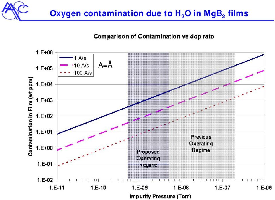
10 Oxygen contamination due to H 2 O in MgB 2 films A=Å
11 Future plans Future work will address the following questions: Can cathodic arc deposition produce high quality MgB 2 thin films in a single step: correct morphology, T c, RRR? Are there better alternatives? (Nb 3 Sn, other candidates)? What are the RF properties of high quality MgB 2 thin films and how are these properties affected by the MgB 2 thin film microstructure? Is a cathodic deposition process that is compatible with deposition of MgB 2 onto Nb and/or Cu RF cavities a possibility?

Coating Technology: Evaporation Vs Sputtering
 Satisloh Italy S.r.l. Coating Technology: Evaporation Vs Sputtering Gianni Monaco, PhD R&D project manager, Satisloh Italy 04.04.2016 V1 The aim of this document is to provide basic technical information
High quality superconducting niobium films produced by Ultra High Vacuum
 High quality superconducting niobium films produced by Ultra High Vacuum Cathodic Arc R. Russo a Dipartimento di Fisica, Università degli studi di Roma Tor Vergata, 00133 Roma, Italy and Istituto di Cibernetica
Vacuum Evaporation Recap
 Sputtering Vacuum Evaporation Recap Use high temperatures at high vacuum to evaporate (eject) atoms or molecules off a material surface. Use ballistic flow to transport them to a substrate and deposit.
A Remote Plasma Sputter Process for High Rate Web Coating of Low Temperature Plastic Film with High Quality Thin Film Metals and Insulators
 A Remote Plasma Sputter Process for High Rate Web Coating of Low Temperature Plastic Film with High Quality Thin Film Metals and Insulators Dr Peter Hockley and Professor Mike Thwaites, Plasma Quest Limited
B I N G O B I N G O. Hf Cd Na Nb Lr. I Fl Fr Mo Si. Ho Bi Ce Eu Ac. Md Co P Pa Tc. Uut Rh K N. Sb At Md H. Bh Cm H Bi Es. Mo Uus Lu P F.
 Hf Cd Na Nb Lr Ho Bi Ce u Ac I Fl Fr Mo i Md Co P Pa Tc Uut Rh K N Dy Cl N Am b At Md H Y Bh Cm H Bi s Mo Uus Lu P F Cu Ar Ag Mg K Thomas Jefferson National Accelerator Facility - Office of cience ducation
Lecture 12. Physical Vapor Deposition: Evaporation and Sputtering Reading: Chapter 12. ECE 6450 - Dr. Alan Doolittle
 Lecture 12 Physical Vapor Deposition: Evaporation and Sputtering Reading: Chapter 12 Evaporation and Sputtering (Metalization) Evaporation For all devices, there is a need to go from semiconductor to metal.
Ion Beam Sputtering: Practical Applications to Electron Microscopy
 Ion Beam Sputtering: Practical Applications to Electron Microscopy Applications Laboratory Report Introduction Electron microscope specimens, both scanning (SEM) and transmission (TEM), often require a
OLED display. Ying Cao
 OLED display Ying Cao Outline OLED basics OLED display A novel method of fabrication of flexible OLED display Potentials of OLED Suitable for thin, lightweight, printable displays Broad color range Good
CVD SILICON CARBIDE. CVD SILICON CARBIDE s attributes include:
 CVD SILICON CARBIDE CVD SILICON CARBIDE is the ideal performance material for design engineers. It outperforms conventional forms of silicon carbide, as well as other ceramics, quartz, and metals in chemical
INFRARED MONITORING OF 110 GHz GYROTRON WINDOWS AT DIII D
 GA A23981 INFRARED MONITORING OF 110 GHz GYROTRON WINDOWS AT DIII D by Y. GORELOV, J. LOHR, R.W. CALLIS, and D. PONCE MAY 2002 DISCLAIMER This report was prepared as an account of work sponsored by an
Deposition of Thin Metal Films " (on Polymer Substrates)!
!") Deposition of Thin Metal Films " (on Polymer Substrates)! Shefford P. Baker! Cornell University! Department of Materials Science and Engineering! Ithaca, New York, 14853! MS&E 5420 Flexible Electronics,
Deposition of Thin Metal Films " (on Polymer Substrates)! Shefford P. Baker! Cornell University! Department of Materials Science and Engineering! Ithaca, New York, 14853! MS&E 5420 Flexible Electronics,
Chapter 4 Indium Tin Oxide Films Deposited by d.c. Sputtering
 Chapter 4 Indium Tin Oxide Films Deposited by d.c. Sputtering 4.1. Introduction Indium-tin-oxide (ITO) thin films are widely used in optoelectronics devices, flat panel display and electrochromic (EC)
MORPHOLOGY OF NIOBIUM FILMS SPUTTERED AT DIFFERENT TARGET SUBSTRATE ANGLE
 MORPHOLOGY OF NIOBIUM FILMS SPUTTERED AT DIFFERENT TARGET SUBSTRATE ANGLE D. Tonini *, C. Greggio, G. Keppel, F. Laviano $, M. Musiani, G. Torzo and V. Palmieri * Università degli Studi di Padova; INFN-LNL
DIEGO TONINI MORPHOLOGY OF NIOBIUM FILMS SPUTTERED AT DIFFERENT TARGET SUBSTRATE ANGLE
 UNIVERSITÀ DEGLI STUDI DI PADOVA SCIENCE FACULTY MATERIAL SCIENCE DEGREE INFN LABORATORI NAZIONALI DI LEGNARO DIEGO TONINI MORPHOLOGY OF NIOBIUM FILMS SPUTTERED AT DIFFERENT TARGET SUBSTRATE ANGLE 2 QUESTIONS
Reactive Sputtering Using a Dual-Anode Magnetron System
 Reactive Sputtering Using a Dual-Anode Magnetron System A. Belkind and Z. Zhao, Stevens Institute of Technology, Hoboken, NJ; and D. Carter, G. McDonough, G. Roche, and R. Scholl, Advanced Energy Industries,
2. Deposition process
 Properties of optical thin films produced by reactive low voltage ion plating (RLVIP) Antje Hallbauer Thin Film Technology Institute of Ion Physics & Applied Physics University of Innsbruck Investigations
High Rate Oxide Deposition onto Web by Reactive Sputtering from Rotatable Magnetrons
 High Rate Oxide Deposition onto Web by Reactive Sputtering from Rotatable Magnetrons D.Monaghan, V. Bellido-Gonzalez, M. Audronis. B. Daniel Gencoa, Physics Rd, Liverpool, L24 9HP, UK. www.gencoa.com,
Optical Properties of Sputtered Tantalum Nitride Films Determined by Spectroscopic Ellipsometry
 Optical Properties of Sputtered Tantalum Nitride Films Determined by Spectroscopic Ellipsometry Thomas Waechtler a, Bernd Gruska b, Sven Zimmermann a, Stefan E. Schulz a, Thomas Gessner a a Chemnitz University
Chem 115 POGIL Worksheet - Week 4 Moles & Stoichiometry Answers
 Key Questions & Exercises Chem 115 POGIL Worksheet - Week 4 Moles & Stoichiometry Answers 1. The atomic weight of carbon is 12.0107 u, so a mole of carbon has a mass of 12.0107 g. Why doesn t a mole of
The interaction of Cu(100)-Fe surfaces with oxygen studied with photoelectron spectroscopy. I
-Fe surfaces with oxygen studied with photoelectron spectroscopy. I") 5 The interaction of Cu(100)-Fe surfaces with oxygen studied with photoelectron spectroscopy. I Mg Kα excited photoemission. Abstract The oxidation of Cu(100)-Fe surfaces was studied using XPS. Surfaces
5 The interaction of Cu(100)-Fe surfaces with oxygen studied with photoelectron spectroscopy. I Mg Kα excited photoemission. Abstract The oxidation of Cu(100)-Fe surfaces was studied using XPS. Surfaces
Chapter 7-1. Definition of ALD
 Chapter 7-1 Atomic Layer Deposition (ALD) Definition of ALD Brief history of ALD ALD process and equipments ALD applications 1 Definition of ALD ALD is a method of applying thin films to various substrates
OPTIMIZING OF THERMAL EVAPORATION PROCESS COMPARED TO MAGNETRON SPUTTERING FOR FABRICATION OF TITANIA QUANTUM DOTS
 OPTIMIZING OF THERMAL EVAPORATION PROCESS COMPARED TO MAGNETRON SPUTTERING FOR FABRICATION OF TITANIA QUANTUM DOTS Vojtěch SVATOŠ 1, Jana DRBOHLAVOVÁ 1, Marian MÁRIK 1, Jan PEKÁREK 1, Jana CHOMOCKÁ 1,
Chem 115 POGIL Worksheet - Week 4 Moles & Stoichiometry
 Chem 115 POGIL Worksheet - Week 4 Moles & Stoichiometry Why? Chemists are concerned with mass relationships in chemical reactions, usually run on a macroscopic scale (grams, kilograms, etc.). To deal with
How do single crystals differ from polycrystalline samples? Why would one go to the effort of growing a single crystal?
 Crystal Growth How do single crystals differ from polycrystalline samples? Single crystal specimens maintain translational symmetry over macroscopic distances (crystal dimensions are typically 0.1 mm 10
3 - Atomic Absorption Spectroscopy
 3 - Atomic Absorption Spectroscopy Introduction Atomic-absorption (AA) spectroscopy uses the absorption of light to measure the concentration of gas-phase atoms. Since samples are usually liquids or solids,
Introduction to vacuum gauges. Vacuum Gauges where the Pressure Readings are Independent of the Type of Gas (Mechanical Vacuum Gauges)
") Introduction to vacuum gauges Vacuum Gauges where the Pressure Readings are Independent of the Type of Gas (Mechanical Vacuum Gauges) BOURDON Vacuum Gauge The inside of a tube which is bent into a circular
Introduction to vacuum gauges Vacuum Gauges where the Pressure Readings are Independent of the Type of Gas (Mechanical Vacuum Gauges) BOURDON Vacuum Gauge The inside of a tube which is bent into a circular
Methods of plasma generation and plasma sources
 Methods of plasma generation and plasma sources PlasTEP trainings course and Summer school 2011 Warsaw/Szczecin Indrek Jõgi, University of Tartu Partfinanced by the European Union (European Regional Development
Crystal Structure of High Temperature Superconductors. Marie Nelson East Orange Campus High School NJIT Professor: Trevor Tyson
 Crystal Structure of High Temperature Superconductors Marie Nelson East Orange Campus High School NJIT Professor: Trevor Tyson Introduction History of Superconductors Superconductors are material which
Nanoparticle Deposition on Packaging Materials by the Liquid Flame Spray
 Nanoparticle Deposition on Packaging Materials by the Liquid Flame Spray Hannu Teisala a, Mikko Tuominen a, Mikko Aromaa b, Jyrki M. Mäkelä b, Milena Stepien c, Jarkko J. Saarinen c, Martti Toivakka c
Deposition of Silicon Oxide, Silicon Nitride and Silicon Carbide Thin Films by New Plasma Enhanced Chemical Vapor Deposition Source Technology
 General Plasma, Inc. 546 East 25th Street Tucson, Arizona 85713 tel. 520-882-5100 fax. 520-882-5165 and Silicon Carbide Thin Films by New Plasma Enhanced Chemical Vapor Deposition Source Technology M.
Chapter 6 Metal Films and Filters
 Chapter 6 Metal Films and Filters 6.1 Mirrors The first films produced by vacuum deposition as we know it were aluminum films for mirrors made by John Strong in the 1930s; he coated mirrors for astronomical
Development of a Low Frequency Superconducting RF Electron Gun. September 2010
 Development of a Low Frequency Superconducting RF Electron Gun Contract DE-FG02-07ER84861 07ER84861 Terry Grimm September 2010 Outline Collaboration Concept Scientific justification Design electromagnetic
Characterization of sputtered NiO thin films
 Surface & Coatings Technology 198 (2005) 138 142 www.elsevier.com/locate/surfcoat Characterization of sputtered NiO thin films Hao-Long Chen a, *, Yang-Ming Lu b, Weng-Sing Hwang a a Department of Materials
Novel inkjettable copper ink utilizing processing temperatures under 100 degrees C without the need of inert atmosphere
 Novel inkjettable copper ink utilizing processing temperatures under 100 degrees C without the need of inert atmosphere Printed Electronics Europe April 7-8, 2009 Dresden, Germany Dr. Zvi Yaniv Applied
State of the art in reactive magnetron sputtering
 State of the art in reactive magnetron sputtering T. Nyberg, O. Kappertz, T. Kubart and S. Berg Solid State Electronics, The Ångström Laboratory, Uppsala University, Box 534, S-751 21 Uppsala, Sweden D.
Improved Contact Formation for Large Area Solar Cells Using the Alternative Seed Layer (ASL) Process
 Process") Improved Contact Formation for Large Area Solar Cells Using the Alternative Seed Layer (ASL) Process Lynne Michaelson, Krystal Munoz, Jonathan C. Wang, Y.A. Xi*, Tom Tyson, Anthony Gallegos Technic Inc.,
Improved Contact Formation for Large Area Solar Cells Using the Alternative Seed Layer (ASL) Process Lynne Michaelson, Krystal Munoz, Jonathan C. Wang, Y.A. Xi*, Tom Tyson, Anthony Gallegos Technic Inc.,
Chemical vapor deposition of novel carbon materials
 Thin Solid Films 368 (2000) 193±197 www.elsevier.com/locate/tsf Chemical vapor deposition of novel carbon materials L. Chow a, b, *, D. Zhou b, c, A. Hussain b, c, S. Kleckley a, K. Zollinger a, A. Schulte
Effect of the oxide film formed on the electrical properties of Cu-Zn alloy electric contact material
 Effect of the oxide film formed on the electrical properties of Cu-Zn alloy electric contact material Hao-Long Chen *, Ke-Cheng Tseng and Yao-Sheng Yang Department of Electronic Engineering, Kao Yuan University,
Modification of Pd-H 2 and Pd-D 2 thin films processed by He-Ne laser
 Modification of Pd-H 2 and Pd-D 2 thin films processed by He-Ne laser V.Nassisi #, G.Caretto #, A. Lorusso #, D.Manno %, L.Famà %, G.Buccolieri %, A.Buccolieri %, U.Mastromatteo* # Laboratory of Applied
Material Development for Electron Beam Melting Timothy Horn Tjhorn.ims@gmail.com
 Material Development for Electron Beam Melting Timothy Horn Tjhorn.ims@gmail.com Center for Additive Manufacturing and Logistics http://camal.ncsu.edu Advantages of Additive Manufacturing Extremely complex
Dry Etching and Reactive Ion Etching (RIE)
") Dry Etching and Reactive Ion Etching (RIE) MEMS 5611 Feb 19 th 2013 Shengkui Gao Contents refer slides from UC Berkeley, Georgia Tech., KU, etc. (see reference) 1 Contents Etching and its terminologies
Dry Etching and Reactive Ion Etching (RIE) MEMS 5611 Feb 19 th 2013 Shengkui Gao Contents refer slides from UC Berkeley, Georgia Tech., KU, etc. (see reference) 1 Contents Etching and its terminologies
Surface characterization of oxygen deficient SrTiO 3
 U. Scotti di Uccio Surface characterization of oxygen deficient SrTiO 3 films and single crystals Coherentia-CNR-INFM Napoli, Italy Prof. R. Vaglio R. Di Capua, G. De Luca, M. Radovic, N. Lampis, P. Perna,
SALES SPECIFICATION. SC7640 Auto/Manual High Resolution Sputter Coater
 SALES SPECIFICATION SC7640 Auto/Manual High Resolution Sputter Coater Document Number SS-SC7640 Issue 1 (01/02) Disclaimer The components and packages described in this document are mutually compatible
Transition from AMR to GMR Heads in Tape Recording
 Transition from AMR to GMR Heads in Tape Recording John P. Nibarger Sun Microsystems 1450 Infinite Dr., Louisville CO 80027-9440 Phone: +1-303-661-2837 FAX: +1-303-661-8992 E-mail: john.nibarger@sun.com
Electron Beam and Sputter Deposition Choosing Process Parameters
 Electron Beam and Sputter Deposition Choosing Process Parameters General Introduction The choice of process parameters for any process is determined not only by the physics and/or chemistry of the process,
Neuere Entwicklungen zur Herstellung optischer Schichten durch reaktive. Wolfgang Hentsch, Dr. Reinhard Fendler. FHR Anlagenbau GmbH
 Neuere Entwicklungen zur Herstellung optischer Schichten durch reaktive Sputtertechnologien Wolfgang Hentsch, Dr. Reinhard Fendler FHR Anlagenbau GmbH Germany Contents: 1. FHR Anlagenbau GmbH in Brief
Electron Charge to Mass Ratio Matthew Norton, Chris Bush, Brian Atinaja, Becker Steven. Norton 0
 Electron Charge to Mass Ratio Matthew Norton, Chris Bush, Brian Atinaja, Becker Steven Norton 0 Norton 1 Abstract The electron charge to mass ratio was an experiment that was used to calculate the ratio
Structure and properties of transparent conductive ZnO films grown by pulsed laser
 Structure and properties of transparent conductive ZnO films grown by pulsed laser deposition (PLD) by Yu Hsiu, Lin A dissertation submitted to the University of Birmingham for the degree of Master of
MECHANICAL AND THERMAL ANALYSES OF THE CABLE/ STRAND STRAIN TEST FIXTURE
 TD-01-001 January 6, 2000 MECHANICAL AND THERMAL ANALYSES OF THE CABLE/ STRAND STRAIN TEST FIXTURE Michela Fratini, Emanuela Barzi Abstract: A fixture to assess the superconducting performance of a reacted
Production of ferrite nanopowders in radiofrequency thermal plasma
 Production of ferrite nanopowders in radiofrequency thermal plasma PhD Theses Loránd Gál Budapest, 2008 HAS Chemical Research Center Institute of Materials and Environmental Chemistry Department of Plasma
CONSOLIDATION AND HIGH STRAIN RATE MECHANICAL BEHAVIOR OF NANOCRYSTALLINE TANTALUM POWDER
 CONSOLIDATION AND HIGH STRAIN RATE MECHANICAL BEHAVIOR OF NANOCRYSTALLINE TANTALUM POWDER Sang H. Yoo, T.S. Sudarshan, Krupa Sethuram Materials Modification Inc, 2929-P1 Eskridge Rd, Fairfax, VA, 22031
Direct Energy Influx Measurements. in Low Pressure Plasma Processes
 Direct Energy Influx Measurements in Low Pressure Plasma Processes A.L. Thomann, GREMI Orléans R. Dussart, N. Semmar, J. Mathias, T. Lecas L. Bedra, P.A. Cormier, V. Dolique Outline I. Introduction: Why
Improvement of surface porosity and properties of alumina films by incorporation of Fe micrograins in micro-arc oxidation
 Applied Surface Science 253 (2006) 863 868 www.elsevier.com/locate/apsusc Improvement of surface porosity and properties of alumina films by incorporation of Fe micrograins in micro-arc oxidation Fanya
Chapter 2 Toward Metallic Butterfly Wing Scales
 Chapter 2 Toward Metallic Butterfly Wing Scales 2.1 Introduction Till now, natural biostructures have already been converted to a broad range of oxides. To prepare these replicas, metal ions were first
Polymer growth rate in a wire chamber with oxygen, water, or alcohol gas additives
 SLAC-PUB-13 June 6, 8 Polymer growth rate in a wire chamber with oxygen, water, or alcohol gas additives Adam M. Boyarski Stanford Linear Accelerator Center, M.S. 95, 575 Sand Hill Rd, Menlo Park, CA 95,
Planar Magnetron Sputtering Sources
 Planar Magnetron puttering ources INTRODUCTION TABLE OF CONTENT PAGE Introduction........................ 2 MAK 1.3...........................3 MAK 2............................4 MAK 3............................5
Sputtering. Ion-Solid Interactions
 ssistant Professor Department of Microelectronic Engineering Rochester Institute of Technology 82 Lomb Memorial Drive Rochester, NY 14623-5604 Tel (716) 475-2923 Fax (716) 475-5041 PDRDV@RIT.EDU Page 1
THE EFFECT OF THE HDDR PROCESS ON THE PRODUCTION OF Pr-Fe-Co-B-Nb SINTERED MAGNETS
 THE EFFECT OF THE HDDR PROCESS ON THE PRODUCTION OF Pr-Fe-Co-B-Nb SINTERED MAGNETS E. A. Ferreira, J. C. S. Casini, E. A. Périgo, R. N. Faria, H. Takiishi Av. Prof. Lineu Prestes, 2242 - CEP 05508-000,
WHITEPAPER ENHANCED REACTIVELY SPUTTERED AL 2 O 3 DEPOSITION BY ADDITION OF ACTIVATED REACTIVE OXYGEN
 WHITEPAPER By D. Carter and G. McDonough of Advanced Energy Industries, Inc. ENHANCED REACTIVELY The impact of preactivation of oxygen in the reactive sputter deposition of Al 2 O 3 is investigated. Oxygen,
III. Wet and Dry Etching
 III. Wet and Dry Etching Method Environment and Equipment Advantage Disadvantage Directionality Wet Chemical Solutions Atmosphere, Bath 1) Low cost, easy to implement 2) High etching rate 3) Good selectivity
Graduate Student Presentations
 Graduate Student Presentations Dang, Huong Chip packaging March 27 Call, Nathan Thin film transistors/ liquid crystal displays April 4 Feldman, Ari Optical computing April 11 Guerassio, Ian Self-assembly
Sputter deposition processes
 Sputter deposition processes D. Depla 1, S. Mahieu 1, J.E. Greene 2 1 Ghent University, Department of Solid State Sciences, Krijgslaan 281 (S1), 9000 Ghent, Belgium 2 Materials Science and Physics Departments
Quantum Computing for Beginners: Building Qubits
 Quantum Computing for Beginners: Building Qubits Suzanne Gildert Condensed Matter Physics Research (Quantum Devices Group) University of Birmingham 28/03/2007 Overview of this presentation What is a Qubit?
Al 2 O 3, Its Different Molecular Structures, Atomic Layer Deposition, and Dielectrics
 Al 2 O 3, Its Different Molecular Structures, Atomic Layer Deposition, and Dielectrics Mark Imus Douglas Sisk, Ph.D., Mentor Marian High School RET Program University of Notre Dame Project Proposal Tunneling
COATED CARBIDE. TiN. Al 2 O 3
 COATED CARBIDE GENERAL INFORMATION CVD = Chemical Vapour Deposition coated grades GC2015, GC2025, GC2135, GC235, GC3005, GC3015, GC3020, GC3025, GC3115, GC4015, GC4025, GC4035, S05F, and CD1810. PVD =
Corrosion experiments in amine solutions
 Corrosion experiments in amine solutions Andreas Grimstvedt Process technology SINTEF Materials and chemistry Wenle He Applied mechanics and corrosion SINTEF Materials and chemistry 1 Contents of presentation
Sputtered AlN Thin Films on Si and Electrodes for MEMS Resonators: Relationship Between Surface Quality Microstructure and Film Properties
 Sputtered AlN Thin Films on and Electrodes for MEMS Resonators: Relationship Between Surface Quality Microstructure and Film Properties S. Mishin, D. R. Marx and B. Sylvia, Advanced Modular Sputtering,
Magnetic Investigation of High Purity Niobium for Superconducting RF Cavities. Proposal for LCRD/UCLC 2005
 Magnetic Investigation of High Purity Niobium for Superconducting RF Cavities Proposal for LCRD/UCLC 2005 Classification (subsystem) Material science on niobium for superconducting cavities of main linac
HPPMS/DC-MSIP (Cr,Al,V)N and (Cr,Al,W)N Thin Films for High Temperature Application
N and (Cr,Al,W)N Thin Films for High Temperature Application") HPPMS/DC-MSIP (Cr,Al,V)N and (Cr,Al,W)N Thin Films for High Temperature Application Sebastian Theiß K. Bobzin, N. Bagcivan, M. Ewering, R. H. Brugnara April 23, 21 HPPMS/HiPIMS/MPP Workshop, Golden Outline
HPPMS/DC-MSIP (Cr,Al,V)N and (Cr,Al,W)N Thin Films for High Temperature Application Sebastian Theiß K. Bobzin, N. Bagcivan, M. Ewering, R. H. Brugnara April 23, 21 HPPMS/HiPIMS/MPP Workshop, Golden Outline
BIOACTIVE COATINGS ON 316L STAINLESS STEEL IMPLANTS
 Trends Biomater. Artif. Organs. Vol. 17(2) pp 43-47 (2004) http//www.sbaoi.org BIOACTIVE COATINGS ON 316L STAINLESS STEEL IMPLANTS N. Ramesh Babu*,+, Sushant Manwatkar*, K. Prasada Rao* and T. S. Sampath
E/M Experiment: Electrons in a Magnetic Field.
 E/M Experiment: Electrons in a Magnetic Field. PRE-LAB You will be doing this experiment before we cover the relevant material in class. But there are only two fundamental concepts that you need to understand.
Cleaning Methods of SRF Power Couplers. Mircea Stirbet
 Cleaning Methods of SRF Power Couplers Mircea Stirbet Principles - The FPC cleaning should start at the design stage - Continue during component manufacture, storage and transportation to the final destination.
7. advanced SEM. Latest generation of SEM SEM
 7. advanced SEM SEM Low voltage SE imaging Condition of the surface, coatings, plasma cleaning Low voltage BSE imaging Polishing for BSE, EDX and EBSD, effect of ion beam etching/polishing 1 Latest generation
Coating Thickness and Composition Analysis by Micro-EDXRF
 Application Note: XRF Coating Thickness and Composition Analysis by Micro-EDXRF www.edax.com Coating Thickness and Composition Analysis by Micro-EDXRF Introduction: The use of coatings in the modern manufacturing
Impurity-doped ZnO Thin Films Prepared by Physical Deposition Methods Appropriate for
 Home Search Collections Journals About Contact us My IOPscience Impurity-doped ZnO Thin Films Prepared by Physical Deposition Methods Appropriate for Transparent Electrode Applications in Thin-film Solar
THIN FILM MATERIALS TECHNOLOGY
 THIN FILM MATERIALS TECHNOLOGY Sputtering of Compound Materials by Kiyotaka Wasa Yokohama City University Yokohama, Japan Makoto Kitabatake Matsushita Electric Industrial Co., Ltd. Kyoto, Japan Hideaki
Non-Inductive Startup and Flux Compression in the Pegasus Toroidal Experiment
 Non-Inductive Startup and Flux Compression in the Pegasus Toroidal Experiment John B. O Bryan University of Wisconsin Madison NIMROD Team Meeting July 31, 2009 Outline 1 Introduction and Motivation 2 Modeling
Damage-free, All-dry Via Etch Resist and Residue Removal Processes
 Damage-free, All-dry Via Etch Resist and Residue Removal Processes Nirmal Chaudhary Siemens Components East Fishkill, 1580 Route 52, Bldg. 630-1, Hopewell Junction, NY 12533 Tel: (914)892-9053, Fax: (914)892-9068
The BESSY HOM Damped Cavity with Ferrite Absorbers. Review of prototype cavity test results, taperedwaveguidesvshomogenouswaveguides
 The BESSY HOM Damped Cavity with Ferrite Absorbers E. Weihreter / BESSY Review of prototype cavity test results, taperedwaveguidesvshomogenouswaveguides Design of a ferrite loaded ridged circular waveguide
For Touch Panel and LCD Sputtering/PECVD/ Wet Processing
 production Systems For Touch Panel and LCD Sputtering/PECVD/ Wet Processing Pilot and Production Systems Process Solutions with over 20 Years of Know-how Process Technology at a Glance for Touch Panel,
Problems in Welding of High Strength Aluminium Alloys
 Singapore Welding Society Newsletter, September 1999 Problems in Welding of High Strength Aluminium Alloys Wei Zhou Nanyang Technological University, Singapore E-mail: WZhou@Cantab.Net Pure aluminium has
Optical Hyperdoping: Transforming Semiconductor Band Structure for Solar Energy Harvesting
 Optical Hyperdoping: Transforming Semiconductor Band Structure for Solar Energy Harvesting 3G Solar Technologies Multidisciplinary Workshop MRS Spring Meeting San Francisco, CA, 5 April 2010 Michael P.
Deposition of Conducting Oxide Thin Films as Anode for Solar Cell Device
 British Journal of Applied Science & Technology 4(5): 739-748, 2014 SCIENCEDOMAIN international www.sciencedomain.org Deposition of Conducting Oxide Thin Films as Anode for Solar Cell Device N. Mustapha
Chemical Sputtering. von Kohlenstoff durch Wasserstoff. W. Jacob
 Chemical Sputtering von Kohlenstoff durch Wasserstoff W. Jacob Centre for Interdisciplinary Plasma Science Max-Planck-Institut für Plasmaphysik, 85748 Garching Content: Definitions: Chemical erosion, physical
The Focused Ion Beam Scanning Electron Microscope: A tool for sample preparation, two and three dimensional imaging. Jacob R.
 The Focused Ion Beam Scanning Electron Microscope: A tool for sample preparation, two and three dimensional imaging Jacob R. Bowen Contents Components of a FIB-SEM Ion interactions Deposition & patterns
SUPERCONDUCTIVITY. PH 318- Introduction to superconductors 1
 SUPERCONDUCTIVITY property of complete disappearance of electrical resistance in solids when they are cooled below a characteristic temperature. This temperature is called transition temperature or critical
FIVE PROJECTS OF HIGH RF POWER INPUT COUPLERS & WINDOWS FOR SRF ACCELERATORS*
 FIVE PROJECTS OF HIGH RF POWER INPUT COUPLERS & WINDOWS FOR SRF ACCELERATORS* Quan-Sheng Shu, Joe Susta, Guangfeng Cheng AMAC International Inc., 12050 Jefferson Ave, Newport News, VA 23606 Abstract Various
Microwave firing of MnZn-ferrites
 Materials Science and Engineering B 106 (2004) 289 294 Microwave firing of MnZn-ferrites V. Tsakaloudi, E. Papazoglou, V.T. Zaspalis Laboratory of Inorganic Materials, Chemical Process Engineering Research
The CVD diamond booklet
 available at: www.diamond-materials.com/download Content 1. General properties of diamond... 2 2. Optical Properties... 4 Optical transparency...4 Absorption coefficient at 10.6 µm...5 Refractive index:
Ultra-high Barrier Plastic. MSE5420 Flexible Electronics Martin Yan, GE Global Research
 Ultra-high Barrier Plastic MSE5420 Flexible Electronics Martin Yan, GE Global Research Outline Introduction to plastic substrate and need for barrier Barrier technologies WVTR measurement technologies
Laser sintering of greens compacts of MoSi 2
 Laser sintering of greens compacts of MoSi 2 G. de Vasconcelos 1, R. Cesar Maia 2, C.A.A.Cairo 3, R. Riva 2, N.A.S.Rodrigues 2, F.C.L.Mello 3 Instituto de Estudos Avançados 1, Instituto Tecnológico de
Zinc Whisker Contamination
 Zinc Whisker Contamination A Paper on the Effect and Abatement of Zinc Whiskers in Data Processing Centers By David Loman, HP Services Abstract This paper describes the phenomenon known as Zinc Whiskers,
Plasma Cleaner: Physics of Plasma
 Plasma Cleaner: Physics of Plasma Nature of Plasma A plasma is a partially ionized gas consisting of electrons, ions and neutral atoms or molecules The plasma electrons are at a much higher temperatures
CHAPTER 21 ELECTROCHEMISTRY
 Chapter 21: Electrochemistry Page 1 CHAPTER 21 ELECTROCHEMISTRY 21-1. Consider an electrochemical cell formed from a Cu(s) electrode submerged in an aqueous Cu(NO 3 ) 2 solution and a Cd(s) electrode submerged
Microhardness study of Ti(C, N) films deposited on S-316 by the Hallow Cathode Discharge Gun
 films deposited on S-316 by the Hallow Cathode Discharge Gun") of Achievements in Materials and Manufacturing Engineering VOLUME 14 ISSUE 1-2 January-February 2006 Microhardness study of Ti(C, N) films deposited on S-316 by the Hallow Cathode Discharge Gun A.J. Novinrooz*,
of Achievements in Materials and Manufacturing Engineering VOLUME 14 ISSUE 1-2 January-February 2006 Microhardness study of Ti(C, N) films deposited on S-316 by the Hallow Cathode Discharge Gun A.J. Novinrooz*,
Solar Energy Discovery Lab
 Solar Energy Discovery Lab Objective Set up circuits with solar cells in series and parallel and analyze the resulting characteristics. Introduction A photovoltaic solar cell converts radiant (solar) energy
Status of High Current Ion Sources. Daniela Leitner Lawrence Berkeley National Laboratory
 http://ecrgroup.lbl.gov Status of High Current Ion Sources Daniela Leitner Lawrence Berkeley National Laboratory October, 27th, 2003 1 Content Overview of available high current sources Requirements for
Special materials. for Precision Optics & Laser Coatings. Oxides for Evaporation
 Special materials for Precision Optics & Laser Coatings Oxides for Evaporation Titanium oxides Highest refractive index of oxides in visible range AR and multilayer coatings on glass and polymers Best
The Three Heat Transfer Modes in Reflow Soldering
 Section 5: Reflow Oven Heat Transfer The Three Heat Transfer Modes in Reflow Soldering There are three different heating modes involved with most SMT reflow processes: conduction, convection, and infrared
The study of deep-level emission center in ZnO films grown on c-al 2 O 3 substrates
 The study of deep-level emission center in ZnO films grown on c-al 2 O 3 substrates Guotong Du Yuantao Zhang, Jinzhong Wang, Yongguo Cui (College of Electronic Science and Engineering, State Key Laboratory