Sensors & Instruments for station. returned samples. Chun Chia Tan
|
|
|
- Elmer Hood
- 8 years ago
- Views:
Transcription
1 Sensors & Instruments for station based materials characterization of returned samples Chun Chia Tan 04/01/2009

2 Outline Introduction to materials characterization General overview of the equipment used to study different material properties X ray photoelectron spectroscopy Atomic force Microscope Scanning electron Microscope

3 Introduction to materials characterization Materials a characterization acte ato Unknown material Examine the chemical composition Arrangement of the atoms Superficial observation of the material Material with known property Understand and quantify the extent in which it exhibits this property Understand why it exhibits this property How can we make use of this material property?

4 Introduction to materials characterization To be able to characterize these materials, we must: Know the material properties we are characterizing Understand how the properties can be identified Understand how the equipment for investigating the material property works

5 Types of material properties for Chemical composition Chemical bonding Material topology Roughness of the material Features of the material surface Crystallization temperatures Crystal structures Electrical properties Magnetic properties Optical propertiesp characterization ti

6 Some equipments used for materials characterization i Different equipments used for materials characterization Differential scanning calorimetry Raman Spectroscopy X ray Diffraction X ray photoelectron spectroscopy Features of a differential scanning calorimetry curve Bragg s Diffraction in XRD

7 Some equipments used for materials characterization Different equipments used for materials characterization Atomic force Microscopy Scanning electron microscopy Transmission electron microscopy AFM: image of a Y junction carbon nanotube. SEM: This grain of kosher salt is composed of many cubes stuck together. TEM: Porous silicon on top of bulk silicon

8 X ray Photoelectron Spectroscopy

9 X ray Photoelectron Spectroscopy XPS is a quantitative spectroscopic technique that measures elemental composition empirical formula chemical state electronic state of the elements which exist in a material XPS spectra is obtained by focusing X rays on the sample material then measuring the kinetic energy of the electrons which are emitted from the surface of the material (top 1 10 nm) due to the X ray. Requires ultra high vacuum conditions Also known as ESCA (Electron Spectroscopy for Chemical analysis)
 due to the X ray.")
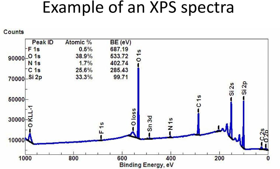
10 Example of an XPS spectra
11 Setup of an XPS machine

12 Electronic Configuration of atoms Every element has a specific arrangement of the energy levels Electrons take up energy levels from the lowest level first S orbitals start to fill up then p orbitals then d orbitals For example, Sodium has 11 electrons, so they will take up the electronic configuration 1s2 2s2 2p6 3s1 Energy Energy level lseparations are 2s different in different atoms 3s 2p 2p 2p E vacuum 1s

13 Band structure of solids Energy Vacuum level Conduction band Fermi Energy Valence band 1 atom 2 atoms Many atoms

14 Emission of photoelectrons X ray photon 3s1 2p6 2s2 1s2 E X ray = hv E kinetic E binding Kinetic Energy of photoelectron Energy at Vacuum level Energy level of 1s electron Electron in 1s2 orbital absorbs the energy from the X ray photon Energy absorbed is high enough to escape the attractive force of the nucleus, ie the electron can escape into the vacuum levell Electron still possesses kinetic energy and this kinetic energy can be measured Input energy of the X ray photon is fixed so we can calculate the binding energy E X ray = E kinetic + E binding E binding = E X ray E kinetic

15 Example of an XPS spectra

16 Assignment Use the NIST database ( to identify the elements in the unknown material. What is the suspected chemical compound? 1200 XPS spectra of unknown material ev Cou unt of Electron ns ev ev ev Observed Binding Energy (ev)

17 Spectroscopy Must be able to isolate and separate the electrons with the energy you want Must be able to focus the electrons of the energy you want Separate for one thing and bring it together for everything else +V 2 +V 1

18 Electron energy analysis: The hemispherical analyzer E kinetic eδv = ri ro r E kinetic E s Effective resolution = ΔE = Δr = 0 r r mean

19 Hemispherical analyzer with retarding field ldlens

20

21 Atomic Force Microscopy
22 Introduction to the Atomic Force Microscope AFM, Atomic Force Microscope is also known as SPM or Scanning Probe Microscopy, AFM s predecessor is the Scanning tunneling microscope. STM was developed in 1981 by G. Binnig and H. Rohrer Both were awarded the 1986 Nobel prize AFM uses a high resolution imaging technique that can resolve features as small as an atomic lattice. Researchers use the AFM to observe and manipulate molecular and atomic level features.
23 Working Principle of AFM AFM works by bringing ga cantilever tip in contact with the surface to be imaged. A repulsive/attractive force from the surface atoms applied to the tip bends the cantilever upwards/downwards. The amount of bending, measured by a laserspot spot reflected from the cantilever on to the photodetector. The amount of bending can be used to calculate the force according to Hooke s Law.
24 Different operating distances between the probe tip and the sample There are many regimes of AFM operations. The force is not measured directly, but calculated by measuring the deflection ofthe lever, andknowing the stiffness ofthe cantilever. Hook s law gives F = kz, where F is the force, k is the stiffness of the lever, and z is the distance the lever is bent.
25 AFM Modes of operation Mode of operation contact mode non contact mode intermittentcontact mode lateral force mode magnetic force thermal scanning Force of interaction strong (repulsive) constant force or constant distance weak (attractive) vibrating probe strong (repulsive) vibrating probe frictional forces exert a torque on the scanning cantilever the magnetic field of the surface is imaged the distribution of the thermal conductivity is imaged
26 Probe tips Probe tips from Veeco (TESP) Resolution of the features depend on the probe tips Sharper tips give the ability to image high aspect ratio images
27 Super sharp AFM tips To create super sharp AFM tips, carbon nano tubes are placed/grown on the tips With sharper tips, we can image finer features with higher resolution As the probes become sharper, the cost of the tip increases and the tips are more fragile. Tips may be broken by the sample during scanning
28 Tip selection Height (nm) Height (nm) Position Using a tip with a large radius could result in incorrect surface imaging If a sharper tip is used, finer features can be observed with more information. Position
29 Carbon Nanotubes Tips
30 Leaders in AFM technology Most of the AFM companies spun out from research institutes and universities Park Scientific (Stanford University) Renamed as Park Systems in 1997 Molecular imaging (Arizona State University) Acquired by Agilent Technologies in 2005 Digital instruments (University of California Santa Barbara) Acquired by Veeco in 2002 For a full history check out:
31 AFM systems dicaliber SPM Dimension 3100 SPM
32 Data storage HDDVDR recorded marks AFM image of a CD
33 CD stamper
34 Data Storage Track edge on metal evaporated evaporated recording tape. Lubrication nodules and surface structure are visible in the topography image (left). The magnetic force image (right) used a lift height of 30 nm, and shows how the bit transitions are related to the virgin magnetic structure. 12 µm scan.
35 Magnetic Force Microscopy S N Tip is coated with a ferromagnetic thin film Non contact mode detecting changes in the resonant frequency of the cantilever induced by the magnetic field's dependence d on tip to sample separation
36 Biology Imaging Red blood cells Large scale (100µm) scan of red blood cells Normal and sickled human red blood cells.
37 Latest developments in AFM Nanolithography technology AFM point and click Nanolithography with the low noise Dimension CL SPM head CP II SPM nanolithography pattern created by anodic oxidation with AFM tip
38 Latest developments in AFM Nano manipulation technology Before After Carbon nanotube manipulation
39 Latest developments in AFM technology Improving positioning accuracy Asylum systems Cypher AFM has positioning accuracies up to 60 picometers in the x, y, z directions Implementing smaller laser dots sizes for deflection measurement Allows smaller cantilevers to be used for high speed AC imaging Small Cantilevers provide much higher resonant frequencies than conventional cantilevers without ih an increase in stiffness. In situ measurement of materials Heat and measure the changes in the materials il
40 Scanning Electron Microscopy
41 Scanning Electron Microscope Operation is in high vacuum Electrons are generated from an electron gun Electrons are focused by electromagnetic lenses into a beam with diameter (0.4 nm to 5 nm) Beam is raster scanned across a sample and the radiation signal is picked up by a detector which generates an image Electron gun Electrostatic/Magnetic lenses Scanning coils Detector
42
43 SEM details Magnification of SEM From x25 to x250,000 Hitachi S 5500 FeSEM x2 million Radiation detected Secondary electrons Backscattered electrons X rays Type of radiation observed depends on the detector inthe SEM Different radiation gives different information Sample can be rotated to view topology from different angles Grayscale images only Where lots of electrons were given off in the direction of the secondary electron detector, the image is bright. Where fewer reached the detector, the image is dark.
44 Reading an SEM image
45 Assignment Find the width of the AFM cantilever (Show Find the width of the AFM cantilever (Show your work)
46 Sample preparation Sample should be conductive if not charge accumulation occurs Charging effects leads to image artifacts t Biological specimens may be examined dbut must be dried
47 Cecropia Moth Scales x15,000 A close up of the scale shows that it is mostly air, adding very little weight to the moth
48 SEM image of the same mosquito
49 Diatoms x2000 Diatoms are tiny single celled plants that live inside a hard shell. Shells can be collected and used as diatomaceous earth in swimming pool filters. Shells allow water to pass through but trap any small dirt particles.
50 Coloured SEM images SEM images are grayscale but can be editted d
51 Backscattered electron images Backscattered electrons give some information i of the elements in the sample Heavy elements (high atomic number) backscatter electrons more strongly than light elements (low atomic number) Heavy elements appear brighter in the image Used to detect contrast between areas with different chemical compositions Top picture: The light spots correspond to the regions of Zirconium (40) in an Aluminum (13) background. Backscattered Electrons Secondary Electrons
52 Leaders in SEM technology FEI and Jeol work mainly on electron microscopes Cost of a FeSEM is $ k Latest development in SEM technology Adding probes for materials characterization Multi beam SEM FIB Table top SEM
53 Probes in SEM Probes used for semiconductor material characterization Reliability/failure study of integrated circuits Nano manipulation ofnano nanostructures
54 Multi beam SEM FIB Focused Ion Beam (FIB) uses a beam of ions to mill the sample in the SEM Allows us to view the cross section of the sample
55 Table top SEM Cost efficient Little space needed dd Quick sample loading time Resolution (30 nm) Ease of operation
56 References Differential scanning calorimetry Wikipedia, the free encyclopedia, Last Retrieved: 03/27/2009 Photoelectron t spectroscopy, h / / t5 Last Retrieved: 03/27/2009 X ray photoelectron spectroscopy, Wikipedia, the free encyclopedia, ray p// p / y_p photoelectron_ spectroscopy, py, Last Retrieved: 03/27/2009 / Photoemission, Last Retrieved: 03/27/2009 AFM principles, Last Retrieved: 03/27/2009 Agilent What is an AFM?, US, t t /i i?content US Last tretrieved: 03/27/2009 Agilent AFM Image Library, Last Retrieved: 03/27/2009 / Atomic Force Microscopy Overview, Last Retrieved: 03/27/2009
57 References Xintex Inc, Nanotechnology Innovations, Last Rti Retrieved: d03/27/2009 Asylum Research, Introducting the Cypher AFM, Last Retrieved: 03/27/2009 SEM Tour slide 20, Last Retrieved: 03/27/2009 Scanning Electron Microscope Wikipedia, the free encyclopedia, Last Retrieved: 03/27/2009 Microangela s Electron Microscope Image Gallery, Last Retrieved: 03/27/2009 SEM Image Gallery, Last Retrieved: 03/27/2009 Nanotechnology at Zyvex, Last Retrieved: 03/27/2009 JEOL JIB 4500 Multi beam SEM FIB, spx, Last Retrieved: 03/27/2009 Phenom Desktop SEM, Last Retrieved: 03/27/2009 Magnetic force Microscopy, htm, Last Retrieved: 03/31/2009
h e l p s y o u C O N T R O L
 contamination analysis for compound semiconductors ANALYTICAL SERVICES B u r i e d d e f e c t s, E v a n s A n a l y t i c a l g r o u p h e l p s y o u C O N T R O L C O N T A M I N A T I O N Contamination
Preface Light Microscopy X-ray Diffraction Methods
 Preface xi 1 Light Microscopy 1 1.1 Optical Principles 1 1.1.1 Image Formation 1 1.1.2 Resolution 3 1.1.3 Depth of Field 5 1.1.4 Aberrations 6 1.2 Instrumentation 8 1.2.1 Illumination System 9 1.2.2 Objective
Nanoelectronics 09. Atsufumi Hirohata Department of Electronics. Quick Review over the Last Lecture
 Nanoelectronics 09 Atsufumi Hirohata Department of Electronics 12:00 Wednesday, 4/February/2015 (P/L 006) Quick Review over the Last Lecture ( Field effect transistor (FET) ): ( Drain ) current increases
Usage of Carbon Nanotubes in Scanning Probe Microscopes as Probe. Keywords: Carbon Nanotube, Scanning Probe Microscope
 International Journal of Arts and Sciences 3(1): 18-26 (2009) CD-ROM. ISSN: 1944-6934 InternationalJournal.org Usage of Carbon Nanotubes in Scanning Probe Microscopes as Probe Bedri Onur Kucukyildirim,
View of ΣIGMA TM (Ref. 1)
") Overview of the FESEM system 1. Electron optical column 2. Specimen chamber 3. EDS detector [Electron Dispersive Spectroscopy] 4. Monitors 5. BSD (Back scatter detector) 6. Personal Computer 7. ON/STANDBY/OFF
Overview of the FESEM system 1. Electron optical column 2. Specimen chamber 3. EDS detector [Electron Dispersive Spectroscopy] 4. Monitors 5. BSD (Back scatter detector) 6. Personal Computer 7. ON/STANDBY/OFF
Use the BET (after Brunauer, Emmett and Teller) equation is used to give specific surface area from the adsorption
 equation is used to give specific surface area from the adsorption") Number of moles of N 2 in 0.129dm 3 = 0.129/22.4 = 5.76 X 10⁻³ moles of N 2 gas Module 8 : Surface Chemistry Objectives Lecture 37 : Surface Characterization Techniques After studying this lecture, you
Number of moles of N 2 in 0.129dm 3 = 0.129/22.4 = 5.76 X 10⁻³ moles of N 2 gas Module 8 : Surface Chemistry Objectives Lecture 37 : Surface Characterization Techniques After studying this lecture, you
Lecture 4 Scanning Probe Microscopy (SPM)
") Lecture 4 Scanning Probe Microscopy (SPM) General components of SPM; Tip --- the probe; Cantilever --- the indicator of the tip; Tip-sample interaction --- the feedback system; Scanner --- piezoelectric
Lecture 4 Scanning Probe Microscopy (SPM) General components of SPM; Tip --- the probe; Cantilever --- the indicator of the tip; Tip-sample interaction --- the feedback system; Scanner --- piezoelectric
Atomic Force Microscopy. Long Phan Nanotechnology Summer Series May 15, 2013
 Atomic Force Microscopy Long Phan Nanotechnology Summer Series May 15, 2013 1 World s Smallest Movie 2 Outline What is AFM? How does AFM Work? 3 Modes: Contact mode Non contact mode Tapping mode Imaging
Near-field scanning optical microscopy (SNOM)
") Adviser: dr. Maja Remškar Institut Jožef Stefan January 2010 1 2 3 4 5 6 Fluorescence Raman and surface enhanced Raman 7 Conventional optical microscopy-limited resolution Two broad classes of techniques
Adviser: dr. Maja Remškar Institut Jožef Stefan January 2010 1 2 3 4 5 6 Fluorescence Raman and surface enhanced Raman 7 Conventional optical microscopy-limited resolution Two broad classes of techniques
Electron Microscopy 3. SEM. Image formation, detection, resolution, signal to noise ratio, interaction volume, contrasts
 Electron Microscopy 3. SEM Image formation, detection, resolution, signal to noise ratio, interaction volume, contrasts 3-1 SEM is easy! Just focus and shoot "Photo"!!! Please comment this picture... Any
STM and AFM Tutorial. Katie Mitchell January 20, 2010
 STM and AFM Tutorial Katie Mitchell January 20, 2010 Overview Scanning Probe Microscopes Scanning Tunneling Microscopy (STM) Atomic Force Microscopy (AFM) Contact AFM Non-contact AFM RHK UHV350 AFM/STM
Microscopy. MICROSCOPY Light Electron Tunnelling Atomic Force RESOLVE: => INCREASE CONTRAST BIODIVERSITY I BIOL1051 MAJOR FUNCTIONS OF MICROSCOPES
 BIODIVERSITY I BIOL1051 Microscopy Professor Marc C. Lavoie marc.lavoie@cavehill.uwi.edu MAJOR FUNCTIONS OF MICROSCOPES MAGNIFY RESOLVE: => INCREASE CONTRAST Microscopy 1. Eyepieces 2. Diopter adjustment
1 Introduction. 1.1 Historical Perspective
 j1 1 Introduction 1.1 Historical Perspective The invention of scanning probe microscopy is considered one of the major advances in materials science since 1950 [1, 2]. Scanning probe microscopy includes
Ion Beam Sputtering: Practical Applications to Electron Microscopy
 Ion Beam Sputtering: Practical Applications to Electron Microscopy Applications Laboratory Report Introduction Electron microscope specimens, both scanning (SEM) and transmission (TEM), often require a
Electron Microscopy SEM and TEM
 Electron Microscopy SEM and TEM Content 1. Introduction: Motivation for electron microscopy 2. Interaction with matter 3. SEM: Scanning Electron Microscopy 3.1 Functional Principle 3.2 Examples 3.3 EDX
The Basics of Scanning Electron Microscopy
 The Basics of Scanning Electron Microscopy The small scanning electron microscope is easy to use because almost every variable is pre-set: the acceleration voltage is always 15kV, it has only a single
5. Scanning Near-Field Optical Microscopy 5.1. Resolution of conventional optical microscopy
 5. Scanning Near-Field Optical Microscopy 5.1. Resolution of conventional optical microscopy Resolution of optical microscope is limited by diffraction. Light going through an aperture makes diffraction
bulk 5. Surface Analysis Why surface Analysis? Introduction Methods: XPS, AES, RBS
 5. Surface Analysis Introduction Methods: XPS, AES, RBS Autumn 2011 Experimental Methods in Physics Marco Cantoni Why surface Analysis? Bulk: structural function Electrical/thermal conduction Volume increases
- particle with kinetic energy E strikes a barrier with height U 0 > E and width L. - classically the particle cannot overcome the barrier
 Tunnel Effect: - particle with kinetic energy E strikes a barrier with height U 0 > E and width L - classically the particle cannot overcome the barrier - quantum mechanically the particle can penetrated
CSCI 4974 / 6974 Hardware Reverse Engineering. Lecture 8: Microscopy and Imaging
 CSCI 4974 / 6974 Hardware Reverse Engineering Lecture 8: Microscopy and Imaging Data Acquisition for RE Microscopy Imaging Registration and stitching Microscopy Optical Electron Scanning Transmission Scanning
Scanning Probe Microscopy
 Ernst Meyer Hans Josef Hug Roland Bennewitz Scanning Probe Microscopy The Lab on a Tip With 117 Figures Mß Springer Contents 1 Introduction to Scanning Probe Microscopy f f.1 Overview 2 f.2 Basic Concepts
CREOL, College of Optics & Photonics, University of Central Florida
 OSE6650 - Optical Properties of Nanostructured Materials Optical Properties of Nanostructured Materials Fall 2013 Class 3 slide 1 Challenge: excite and detect the near field Thus far: Nanostructured materials
Nano-Spectroscopy. Solutions AFM-Raman, TERS, NSOM Chemical imaging at the nanoscale
 Nano-Spectroscopy Solutions AFM-Raman, TERS, NSOM Chemical imaging at the nanoscale Since its introduction in the early 80 s, Scanning Probe Microscopy (SPM) has quickly made nanoscale imaging an affordable
Physics 30 Worksheet # 14: Michelson Experiment
 Physics 30 Worksheet # 14: Michelson Experiment 1. The speed of light found by a Michelson experiment was found to be 2.90 x 10 8 m/s. If the two hills were 20.0 km apart, what was the frequency of the
Basic principles and mechanisms of NSOM; Different scanning modes and systems of NSOM; General applications and advantages of NSOM.
 Lecture 16: Near-field Scanning Optical Microscopy (NSOM) Background of NSOM; Basic principles and mechanisms of NSOM; Basic components of a NSOM; Different scanning modes and systems of NSOM; General
Raman spectroscopy Lecture
 Raman spectroscopy Lecture Licentiate course in measurement science and technology Spring 2008 10.04.2008 Antti Kivioja Contents - Introduction - What is Raman spectroscopy? - The theory of Raman spectroscopy
EDS system. CRF Oxford Instruments INCA CRF EDAX Genesis EVEX- NanoAnalysis Table top system
 EDS system Most common X-Ray measurement system in the SEM lab. Major elements (10 wt% or greater) identified in ~10 secs. Minor elements identifiable in ~100 secs. Rapid qualitative and accurate quantitative
Lecture 6 Scanning Tunneling Microscopy (STM) General components of STM; Tunneling current; Feedback system; Tip --- the probe.
 General components of STM; Tunneling current; Feedback system; Tip --- the probe.") Lecture 6 Scanning Tunneling Microscopy (STM) General components of STM; Tunneling current; Feedback system; Tip --- the probe. Brief Overview of STM Inventors of STM The Nobel Prize in Physics 1986 Nobel
Lecture 6 Scanning Tunneling Microscopy (STM) General components of STM; Tunneling current; Feedback system; Tip --- the probe. Brief Overview of STM Inventors of STM The Nobel Prize in Physics 1986 Nobel
Atomic Force Microscopy Observation and Characterization of a CD Stamper, Lycopodium Spores, and Step-Height Standard Diffraction Grating
 Atomic Force Microscopy Observation and Characterization of a CD Stamper, Lycopodium Spores, and Step-Height Standard Diffraction Grating Michael McMearty and Frit Miot Special Thanks to Brendan Cross
Microscopy: Principles and Advances
 Microscopy: Principles and Advances Chandrashekhar V. Kulkarni University of Central Lancashire, Preston, United kingdom May, 2014 University of Ljubljana Academic Background 2005-2008: PhD-Chemical Biology
Phase Characterization of TiO 2 Powder by XRD and TEM
 Kasetsart J. (Nat. Sci.) 42 : 357-361 (28) Phase Characterization of TiO 2 Powder by XRD and TEM Kheamrutai Thamaphat 1 *, Pichet Limsuwan 1 and Boonlaer Ngotawornchai 2 ABSTRACT In this study, the commercial
Chapter 4. Microscopy, Staining, and Classification. Lecture prepared by Mindy Miller-Kittrell North Carolina State University
 Chapter 4 Microscopy, Staining, and Classification 2012 Pearson Education Inc. Lecture prepared by Mindy Miller-Kittrell North Carolina State University Microscopy and Staining 2012 Pearson Education Inc.
How To Understand Light And Color
 PRACTICE EXAM IV P202 SPRING 2004 1. In two separate double slit experiments, an interference pattern is observed on a screen. In the first experiment, violet light (λ = 754 nm) is used and a second-order
Keysight Technologies How to Choose your MAC Lever. Technical Overview
 Keysight Technologies How to Choose your MAC Lever Technical Overview Introduction Atomic force microscopy (AFM) is a sub-nanometer scale imaging and measurement tool that can be used to determine a sample
NEAR FIELD OPTICAL MICROSCOPY AND SPECTROSCOPY WITH STM AND AFM PROBES
 Vol. 93 (1997) A CTA PHYSICA POLONICA A No. 2 Proceedings of the 1st International Symposium on Scanning Probe Spectroscopy and Related Methods, Poznań 1997 NEAR FIELD OPTICAL MICROSCOPY AND SPECTROSCOPY
7/3/2014. Introduction to Atomic Force Microscope. Introduction to Scanning Force Microscope. Invention of Atomic Force Microscope (AFM)
") Introduction to Atomic Force Microscope Introduction to Scanning Force Microscope Not that kind of atomic Tien Ming Chuang ( 莊 天 明 ) Institute of Physics, Academia Sinica Tien Ming Chuang ( 莊 天 明 ) Institute
Introduction to Atomic Force Microscope Introduction to Scanning Force Microscope Not that kind of atomic Tien Ming Chuang ( 莊 天 明 ) Institute of Physics, Academia Sinica Tien Ming Chuang ( 莊 天 明 ) Institute
X-Rays and Magnetism From Fundamentals to Nanoscale Dynamics
 X-Rays and Magnetism From Fundamentals to Nanoscale Dynamics Joachim Stöhr Stanford Synchrotron Radiation Laboratory X-rays have come a long way 1895 1993 10 cm 10 µm 100 nm Collaborators: SSRL Stanford:
Piezoelectric Scanners
 Piezoelectric Scanners Piezoelectric materials are ceramics that change dimensions in response to an applied voltage and conversely, they develop an electrical potential in response to mechanical pressure.
Electron spectroscopy Lecture 1-21. Kai M. Siegbahn (1918 - ) Nobel Price 1981 High resolution Electron Spectroscopy
 Nobel Price 1981 High resolution Electron Spectroscopy") Electron spectroscopy Lecture 1-21 Kai M. Siegbahn (1918 - ) Nobel Price 1981 High resolution Electron Spectroscopy 653: Electron Spectroscopy urse structure cture 1. Introduction to electron spectroscopies
Electron spectroscopy Lecture 1-21 Kai M. Siegbahn (1918 - ) Nobel Price 1981 High resolution Electron Spectroscopy 653: Electron Spectroscopy urse structure cture 1. Introduction to electron spectroscopies
Electromagnetic Radiation (EMR) and Remote Sensing
 and Remote Sensing") Electromagnetic Radiation (EMR) and Remote Sensing 1 Atmosphere Anything missing in between? Electromagnetic Radiation (EMR) is radiated by atomic particles at the source (the Sun), propagates through
Electromagnetic Radiation (EMR) and Remote Sensing 1 Atmosphere Anything missing in between? Electromagnetic Radiation (EMR) is radiated by atomic particles at the source (the Sun), propagates through
Experiment #5: Qualitative Absorption Spectroscopy
 Experiment #5: Qualitative Absorption Spectroscopy One of the most important areas in the field of analytical chemistry is that of spectroscopy. In general terms, spectroscopy deals with the interactions
Physics 441/2: Transmission Electron Microscope
 Physics 441/2: Transmission Electron Microscope Introduction In this experiment we will explore the use of transmission electron microscopy (TEM) to take us into the world of ultrasmall structures. This
Atomic Force Microscope and Magnetic Force Microscope Background Information
 Atomic Force Microscope and Magnetic Force Microscope Background Information Lego Building Instructions There are several places to find the building instructions for building the Lego models of atomic
Chemical Synthesis. Overview. Chemical Synthesis of Nanocrystals. Self-Assembly of Nanocrystals. Example: Cu 146 Se 73 (PPh 3 ) 30
 30") Chemical Synthesis Spontaneous organization of molecules into stable, structurally well-defined aggregates at the nanometer length scale. Overview The 1-100 nm nanoscale length is in between traditional
Chemical Synthesis Spontaneous organization of molecules into stable, structurally well-defined aggregates at the nanometer length scale. Overview The 1-100 nm nanoscale length is in between traditional
Reflection Electron Microscopy and Spectroscopy for Surface Analysis
 Reflection Electron Microscopy and Spectroscopy for Surface Analysis by Zhong Lin Wang 1 Introduction In 1986, E. Ruska was awarded the Nobel Physics Prize for his pioneering work of building the world's
ATOMIC FORCE MICROSCOPY
 ATOMIC FORCE MICROSCOPY Introduction The atomic force microscope, or AFM, is a member of the family of instruments known as scanning probe microscopes. The AFM operates under a completely different principle
BNG 331 Cell-Tissue Material Interactions. Biomaterial Surfaces
 BNG 331 Cell-Tissue Material Interactions Biomaterial Surfaces Course update Updated syllabus Homework 4 due today LBL 5 Friday Schedule for today: Chapter 8 Biomaterial surface characterization Surface
It has long been a goal to achieve higher spatial resolution in optical imaging and
 Nano-optical Imaging using Scattering Scanning Near-field Optical Microscopy Fehmi Yasin, Advisor: Dr. Markus Raschke, Post-doc: Dr. Gregory Andreev, Graduate Student: Benjamin Pollard Department of Physics,
PHYSICAL METHODS, INSTRUMENTS AND MEASUREMENTS Vol. III - Surface Characterization - Marie-Geneviève Barthés-Labrousse
 SURFACE CHARACTERIZATION Marie-Geneviève Centre d Etudes de Chimie Métallurgique, CNRS, Vitry-sur-Seine, France Keywords: Surface Analysis, Surface imaging, Surface composition, Surface chemical analysis,
USING CDs AND DVDs AS DIFFRACTION GRATINGS
 USING CDs AND DVDs AS DIFFRACTION GRATINGS Rama Balachandran Riverwood High School Atlanta, GA Karen Porter-Davis Chamblee Charter High School Chamblee, GA Copyright Georgia Institute of Technology 2009
Highlights of Solid State Physics. Man of the Year Nobel Prizes
 Highlights of Solid State Physics Man of the Year Nobel Prizes Silicon Technology Moore s Law Gordon Moore Intel Jack Kilby 14 nm 2014 Physics Nobel Prize 2000 Integrated Circuit Electrons in the Conduction
Lara Lama laral@kth.se. Axel Nordström axenor@kth.se. Supervisors: Jan Linnros Ilya Sychugov
 Photoluminescence and AFM characterization of silicon nanocrystals prepared by low-temperature plasma enhanced chemical vapour deposition and annealing Lara Lama laral@kth.se Axel Nordström axenor@kth.se
Vacuum Evaporation Recap
 Sputtering Vacuum Evaporation Recap Use high temperatures at high vacuum to evaporate (eject) atoms or molecules off a material surface. Use ballistic flow to transport them to a substrate and deposit.
SPM 150 Aarhus with KolibriSensor
 Customied Systems and Solutions Nanostructures and Thin Film Deposition Surface Analysis and Preparation Components Surface Science Applications SPM 150 Aarhus with KolibriSensor Atomic resolution NC-AFM
Introduktion til røntgenfluorescens (XRF) og skanning elektron mikroskopi (SEM) Michelle Taube Nationalmuseet Bevaringsafdelingen
 og skanning elektron mikroskopi (SEM) Michelle Taube Nationalmuseet Bevaringsafdelingen") Introduktion til røntgenfluorescens (XRF) og skanning elektron mikroskopi (SEM) Michelle Taube Nationalmuseet Bevaringsafdelingen Introduktion til røntgenfluorescens (XRF) og skanning elektron mikroskopi
Introduktion til røntgenfluorescens (XRF) og skanning elektron mikroskopi (SEM) Michelle Taube Nationalmuseet Bevaringsafdelingen Introduktion til røntgenfluorescens (XRF) og skanning elektron mikroskopi
SEM/FIB Workbench. Klocke Nanotechnik. Microtechnology Network. Motion from the Nanoworld. One of 279 members in a. Pascalstr. 17 Aachen, Germany
 Intro_0 SEM/FIB Workbench Motion from the Nanoworld One of 279 members in a Pascalstr. 17 Aachen, Germany Microtechnology Network Centimeter Stroke Atomic Resolution Modular Nanorobotics Modular Nanorobotics
Cathode Ray Tube. Introduction. Functional principle
 Introduction The Cathode Ray Tube or Braun s Tube was invented by the German physicist Karl Ferdinand Braun in 897 and is today used in computer monitors, TV sets and oscilloscope tubes. The path of the
Forms of Energy. Freshman Seminar
 Forms of Energy Freshman Seminar Energy Energy The ability & capacity to do work Energy can take many different forms Energy can be quantified Law of Conservation of energy In any change from one form
ILLUSTRATIVE EXAMPLE: Given: A = 3 and B = 4 if we now want the value of C=? C = 3 + 4 = 9 + 16 = 25 or 2
 Forensic Spectral Anaylysis: Warm up! The study of triangles has been done since ancient times. Many of the early discoveries about triangles are still used today. We will only be concerned with the "right
Scanning Electron Microscopy Primer
 Scanning Electron Microscopy Primer Bob Hafner This primer is intended as background for the Introductory Scanning Electron Microscopy training offered by the University of Minnesota s Characterization
1. Photon Beam Damage and Charging at Solid Surfaces John H. Thomas III
 1. Photon Beam Damage and Charging at Solid Surfaces John H. Thomas III 1. Introduction............................. 2. Electrostatic Charging of Samples in Photoemission Experiments............................
INTRODUCTION TO SCANNING TUNNELING MICROSCOPY
 INTRODUCTION TO SCANNING TUNNELING MICROSCOPY SECOND EDITION C. JULIAN CHEN Department of Applied Physics and Applied Mathematics, Columbia University, New York OXJORD UNIVERSITY PRESS Contents Preface
Lenses and Apertures of A TEM
 Instructor: Dr. C.Wang EMA 6518 Course Presentation Lenses and Apertures of A TEM Group Member: Anup Kr. Keshri Srikanth Korla Sushma Amruthaluri Venkata Pasumarthi Xudong Chen Outline Electron Optics
Unit 12 Practice Test
 Name: Class: Date: ID: A Unit 12 Practice Test Multiple Choice Identify the choice that best completes the statement or answers the question. 1) A solid has a very high melting point, great hardness, and
Indiana's Academic Standards 2010 ICP Indiana's Academic Standards 2016 ICP. map) that describe the relationship acceleration, velocity and distance.
 that describe the relationship acceleration, velocity and distance.") .1.1 Measure the motion of objects to understand.1.1 Develop graphical, the relationships among distance, velocity and mathematical, and pictorial acceleration. Develop deeper understanding through representations
.1.1 Measure the motion of objects to understand.1.1 Develop graphical, the relationships among distance, velocity and mathematical, and pictorial acceleration. Develop deeper understanding through representations
UNIT I: INTRFERENCE & DIFFRACTION Div. B Div. D Div. F INTRFERENCE
 107002: EngineeringPhysics Teaching Scheme: Lectures: 4 Hrs/week Practicals-2 Hrs./week T.W.-25 marks Examination Scheme: Paper-50 marks (2 hrs) Online -50marks Prerequisite: Basics till 12 th Standard
Raman and AFM characterization of carbon nanotube polymer composites Illia Dobryden
 Raman and AFM characterization of carbon nanotube polymer composites Illia Dobryden This project is conducted in High Pressure Spectroscopy Laboratory (Materials Physics group) Supervisor: Professor Alexander
Nanometer-scale imaging and metrology, nano-fabrication with the Orion Helium Ion Microscope
 andras@nist.gov Nanometer-scale imaging and metrology, nano-fabrication with the Orion Helium Ion Microscope Bin Ming, András E. Vladár and Michael T. Postek National Institute of Standards and Technology
Simultaneous data fitting in ARXPS
 NOTE Please find the following more updated document Resolving overlapping peaks in ARXPS data: The effect of noise and fitting method. J. Muñoz-Flores, A. Herrera-Gomez, J. Electron Spectrosc. Relat.
Mass production, R&D Failure analysis. Fault site pin-pointing (EM, OBIRCH, FIB, etc. ) Bottleneck Physical science analysis (SEM, TEM, Auger, etc.
 Bottleneck Physical science analysis (SEM, TEM, Auger, etc.") Failure Analysis System for Submicron Semiconductor Devices 68 Failure Analysis System for Submicron Semiconductor Devices Munetoshi Fukui Yasuhiro Mitsui, Ph. D. Yasuhiko Nara Fumiko Yano, Ph. D. Takashi
Failure Analysis System for Submicron Semiconductor Devices 68 Failure Analysis System for Submicron Semiconductor Devices Munetoshi Fukui Yasuhiro Mitsui, Ph. D. Yasuhiko Nara Fumiko Yano, Ph. D. Takashi
Atomic Force Microscopy. July, 2011 R. C. Decker and S. Qazi
 Atomic Force Microscopy July, 2011 R. C. Decker and S. Qazi Learning through Visualization Visualization of physical phenomena can confirm hypothesis Observation provides opportunities for study without
AS COMPETITION PAPER 2008
 AS COMPETITION PAPER 28 Name School Town & County Total Mark/5 Time Allowed: One hour Attempt as many questions as you can. Write your answers on this question paper. Marks allocated for each question
SILA Sistema Integrato di Laboratori per l Ambiente. CENTRE FOR MICROSCOPY AND MICROANALYSIS Scientific coordinator: Prof.ssa Rosanna De Rosa
 CENTRE FOR MICROSCOPY AND MICROANALYSIS Scientific coordinator: Prof.ssa Rosanna De Rosa 0 The Centre for Microscopy and Microanalysis (CM2) is an interdisciplinary service centre, a comprehensive suite
Time out states and transitions
 Time out states and transitions Spectroscopy transitions between energy states of a molecule excited by absorption or emission of a photon hn = DE = E i - E f Energy levels due to interactions between
(Nano)materials characterization
materials characterization") (Nano)materials characterization MTX9100 Nanomaterials Lecture 8 OUTLINE 1 -What SEM and AFM are good for? - What is the Atomic Force Microscopes Contribution to Nanotechnology? - What is Spectroscopy?
(Nano)materials characterization MTX9100 Nanomaterials Lecture 8 OUTLINE 1 -What SEM and AFM are good for? - What is the Atomic Force Microscopes Contribution to Nanotechnology? - What is Spectroscopy?
Chapter 2: Forms of Energy
 Chapter 2: Forms of Energy Goals of Period 2 Section 2.1: To describe the forms of energy Section 2.2: To illustrate conversions from one form of energy to another Section 2.3: To define the efficiency
LabRAM HR. Research Raman Made Easy! Raman Spectroscopy Systems. Spectroscopy Suite. Powered by:
 LabRAM HR Research Raman Made Easy! Raman Spectroscopy Systems Powered by: Spectroscopy Suite Cutting-Edge Applications with the LabRAM HR Deeply involved in Raman spectroscopy for decades, HORIBA Scientific
3D Raman Imaging Nearfield-Raman TERS. Solutions for High-Resolution Confocal Raman Microscopy. www.witec.de
 3D Raman Imaging Nearfield-Raman TERS Solutions for High-Resolution Confocal Raman Microscopy www.witec.de 01 3D Confocal Raman Imaging Outstanding performance in speed, sensitivity, and resolution with
Tutorial 4.6 Gamma Spectrum Analysis
 Tutorial 4.6 Gamma Spectrum Analysis Slide 1. Gamma Spectrum Analysis In this module, we will apply the concepts that were discussed in Tutorial 4.1, Interactions of Radiation with Matter. Slide 2. Learning
DNA NANOWIRES USING NANOPARTICLES ECG653 Project Report submitted by GOPI KRISHNA.ARI,arig@unlv.nevada.edu,Fall-2008
 DNA NANOWIRES USING NANOPARTICLES ECG653 Project Report submitted by GOPI KRISHNA.ARI,arig@unlv.nevada.edu,Fall-2008 INTRODUCTION: Deoxyribonucleic acid (DNA) has been a key building block in nanotechnology
Christine E. Hatch University of Nevada, Reno
 Christine E. Hatch University of Nevada, Reno Roadmap What is DTS? How Does it Work? What Can DTS Measure? Applications What is Distributed Temperature Sensing (DTS)? Temperature measurement using only
Atomic Force Microscope
 Atomic Force Microscope (Veeco Nanoman) User Manual Basic Operation 4 th Edition Aug 2012 NR System Startup If the system is currently ON To start the NanoScope software, double-click the NanoScope startup
Name Class Date. What is ionic bonding? What happens to atoms that gain or lose electrons? What kinds of solids are formed from ionic bonds?
 CHAPTER 1 2 Ionic Bonds SECTION Chemical Bonding BEFORE YOU READ After you read this section, you should be able to answer these questions: What is ionic bonding? What happens to atoms that gain or lose
Sputtered AlN Thin Films on Si and Electrodes for MEMS Resonators: Relationship Between Surface Quality Microstructure and Film Properties
 Sputtered AlN Thin Films on and Electrodes for MEMS Resonators: Relationship Between Surface Quality Microstructure and Film Properties S. Mishin, D. R. Marx and B. Sylvia, Advanced Modular Sputtering,
MISCIBILITY AND INTERACTIONS IN CHITOSAN AND POLYACRYLAMIDE MIXTURES
 MISCIBILITY AND INTERACTIONS IN CHITOSAN AND POLYACRYLAMIDE MIXTURES Katarzyna Lewandowska Faculty of Chemistry Nicolaus Copernicus University, ul. Gagarina 7, 87-100 Toruń, Poland e-mail: reol@chem.umk.pl
vii TABLE OF CONTENTS CHAPTER TITLE PAGE DECLARATION DEDICATION ACKNOWLEDGEMENT ABSTRACT ABSTRAK
 vii TABLE OF CONTENTS CHAPTER TITLE PAGE DECLARATION DEDICATION ACKNOWLEDGEMENT ABSTRACT ABSTRAK TABLE OF CONTENTS LIST OF TABLES LIST OF FIGURES LIST OF SYMBOLS / ABBREVIATIONS LIST OF APPENDICES ii iii
Keywords: Planar waveguides, sol-gel technology, transmission electron microscopy
 Structural and optical characterisation of planar waveguides obtained via Sol-Gel F. Rey-García, C. Gómez-Reino, M.T. Flores-Arias, G.F. De La Fuente, W. Assenmacher, W. Mader ABSTRACT Planar waveguides
Scanning probe microscopy AFM, STM. Near field Scanning Optical Microscopy(NSOM) Scanning probe fabrication
 Scanning probe fabrication") Scanning probe microscopy AFM, STM Near field Scanning Optical Microscopy(NSOM) Scanning probe fabrication Scanning Probe Microscopy 1986 Binning and Rohrer shared Nobel Prize in Physics for invention.stm
Scanning probe microscopy AFM, STM Near field Scanning Optical Microscopy(NSOM) Scanning probe fabrication Scanning Probe Microscopy 1986 Binning and Rohrer shared Nobel Prize in Physics for invention.stm
Flame Tests & Electron Configuration
 Flame Tests & Electron Configuration INTRODUCTION Many elements produce colors in the flame when heated. The origin of this phenomenon lies in the arrangement, or configuration of the electrons in the
Le nanotecnologie: dal Laboratorio al Mercato. Fabrizio Pirri Politecnico di Torino Istituto Italiano di Tecnologia
 Le nanotecnologie: dal Laboratorio al Mercato Fabrizio Pirri Politecnico di Torino Istituto Italiano di Tecnologia Materials & Processes for micro nanotechnologies Laboratory http://www.polito.it/micronanotech
PHYS 222 Spring 2012 Final Exam. Closed books, notes, etc. No electronic device except a calculator.
 PHYS 222 Spring 2012 Final Exam Closed books, notes, etc. No electronic device except a calculator. NAME: (all questions with equal weight) 1. If the distance between two point charges is tripled, the
Microscopic Techniques
 Microscopic Techniques Outline 1. Optical microscopy Conventional light microscopy, Fluorescence microscopy, confocal/multiphoton microscopy and Stimulated emission depletion microscopy 2. Scanning probe
UNIVERSITY OF SOUTHAMPTON. Scanning Near-Field Optical Microscope Characterisation of Microstructured Optical Fibre Devices.
 UNIVERSITY OF SOUTHAMPTON Scanning Near-Field Optical Microscope Characterisation of Microstructured Optical Fibre Devices. Christopher Wyndham John Hillman Submitted for the degree of Doctor of Philosophy
Optical Microscope; Scanning Electron Microscope (SEM); Transmission Electron Microscope (TEM);
; Transmission Electron Microscope (TEM);") Lecture 3 Brief Overview of Traditional Microscopes Optical Microscope; Scanning Electron Microscope (SEM); Transmission Electron Microscope (TEM); Comparison with scanning probe microscope (SPM) General
Lecture 3 Brief Overview of Traditional Microscopes Optical Microscope; Scanning Electron Microscope (SEM); Transmission Electron Microscope (TEM); Comparison with scanning probe microscope (SPM) General
for Low power Energy Harvesting Sun to fiber' Solar Devices
 Nanostructured Energy Conversion for Low power Energy Harvesting Devices and Beyond for High power Sun to fiber' Solar Devices Michael Oye and Nobuhiko Nobby Kobayashi Advanced Studies Laboratories and
Scanning Electron Microscopy Services for Pharmaceutical Manufacturers
 Scanning Electron Microscopy Services for Pharmaceutical Manufacturers Author: Gary Brake, Marketing Manager Date: August 1, 2013 Analytical Testing Laboratory www.atl.semtechsolutions.com Scanning Electron
CHEMISTRY STANDARDS BASED RUBRIC ATOMIC STRUCTURE AND BONDING
 CHEMISTRY STANDARDS BASED RUBRIC ATOMIC STRUCTURE AND BONDING Essential Standard: STUDENTS WILL UNDERSTAND THAT THE PROPERTIES OF MATTER AND THEIR INTERACTIONS ARE A CONSEQUENCE OF THE STRUCTURE OF MATTER,
WEEKLY COURSE SCHEDULE : PRIMARY EDUCATION
 WEEKLY COURSE SCHEDULE : PRIMARY EDUCATION Semester 1 Week 1 ( 19.09.2011-23.09.2011 ) Introduction to sol-gel processes Properties of X-Rays General Explanations on Process Planning Introduction Semester
Scanning Electron Microscopy: an overview on application and perspective
 Scanning Electron Microscopy: an overview on application and perspective Elvio Carlino Center for Electron Microscopy - IOM-CNR Laboratorio Nazionale TASC - Trieste, Italy Location of the Center for Electron
Counting and imaging bacteria using fluorescent microscopy & Electron Microscopy and Atomic Force Microscopy (AFM)
") Counting and imaging bacteria using fluorescent microscopy & Electron Microscopy and Atomic Force Microscopy (AFM) Bruce E. Logan Kappe Professor of Environmental Engineering Department of Civil and Environmental
Counting and imaging bacteria using fluorescent microscopy & Electron Microscopy and Atomic Force Microscopy (AFM) Bruce E. Logan Kappe Professor of Environmental Engineering Department of Civil and Environmental