Understanding and Characterizing Timing Jitter. Primer
|
|
|
- Lionel McGee
- 8 years ago
- Views:
Transcription
1 Understanding and Characterizing Timing Jitter Primer
2 Primer Table of Contents Introduction...3 Section 1: The Consequences of Jitter...3 Computer Bus Design...3 Serial Data Link...4 Section 2: Just What Is Jitter? Defining Short-Term: Jitter vs. Wander Defining Significant Instants: The Reference Level Defining Ideal Positions: Clock Recovery Period Jitter, Cycle-Cycle Jitter, and TIE...6 Section 3: Jitter Measurement and Visualization Jitter Statistics Jitter Histogram Jitter vs. Time (Time Trend) Jitter vs. Frequency (Jitter Spectrum) Eye Diagram...12 Section 4: Jitter Separation Motivations for Decomposing Jitter The Jitter Model Random Jitter Deterministic Jitter Periodic Jitter Data-Dependent Jitter Duty-Cycle Dependent Jitter Bounded Uncorrelated Jitter Sub-Rate Jitter Putting It All Together...18 Section 5: Jitter vs. Bit Error Rate The Jitter Budget The Bathtub Curve A BER Example...22 Section 6: Summary...23 Appendix A: Glossary of Acronyms...23 References

3 Understanding and Characterizing Timing Jitter Introduction Timing jitter is the unwelcome companion of all electrical systems that use voltage transitions to represent timing information. Historically, electrical systems have lessened the ill effects of timing jitter (or, simply jitter ) by employing relatively low signaling rates. As a consequence, jitter-induced errors have been small when compared with the time intervals that they corrupt. The timing margins associated with today s highspeed serial buses and data links reveal that a tighter control of jitter is needed throughout the system design. As signaling rates climb above 2 GHz and voltage swings shrink to conserve power, the timing jitter in a system becomes a significant percentage of the signaling interval. Under these circumstances, jitter becomes a fundamental performance limit. Understanding what jitter is, and how to characterize it, is the first step to successfully deploying high-speed systems that dependably meet their performance requirements. A more thorough definition will be introduced in Section 2, but conceptually, jitter is the deviation of timing edges from their correct locations. In a timing-based system, timing jitter is the most obvious and direct form of non-idealness. As a form of noise, jitter must be treated as a random process and characterized in terms of its statistics. If you have a way to measure jitter statistics, you can compare components and systems to each other and to chosen limits. However, this alone will not allow you to efficiently refine and debug a cutting-edge design. Only by thoroughly analyzing jitter is it possible for the root causes to be isolated, so that they can be reduced systematically rather than by trial and error. This analysis takes the form of jitter visualization and decomposition, discussed in detail in Sections 3 and 4. Although there are many similarities between the causes, behavior and characterization of electrical and optical jitter, the equipment used to measure jitter in optical systems differs from that used in electrical systems. This paper focuses primarily on jitter in electrical systems. Section 1: The Consequences of Jitter To guess is cheap. To guess wrong is expensive. - Chinese Proverb Why should you be concerned about jitter? What impact does jitter have on system performance? In this section, two cases are considered: a high-speed computer bus, and a serial data link. For each case, the specific effects of jitter are considered in some detail. Computer Bus Design Let s say you are bringing up a new embedded processor design, and are seeing occasional data errors when reading flash memory. You suspect that the address decode that generates the flash memory s chip enable (CE) is not meeting it s setup time requirement with respect to the rising edge of the write enable (WE). You probe the CE and WE signals with your high-speed scope to observe the timing relationship. After ten single-shot acquisitions, you have measured durations of 87 to 92 nsec, all above the minimum setup time of 75 nsec by what seems like a comfortable margin. But what is an adequate margin? Are these times great enough to remove doubt that you are sometimes violating the setup-time requirement? What percent of the time is a violation likely to occur? After evaluating several million waveforms in infinitepersistence mode and seeing setup times as short as 82 nsec, you decide that the setup time might be a problem after all. But is the problem due to variations in the system clock period, in the address decoder, or somewhere else? 3

4 Primer Serial Data Link Your Gigabit Ethernet physical-layer transceiver chip is pushing up against deadline and you are a bit nervous about the compliance tests that will soon be run by an external test house. The spec in the standards document calls for a measurement of data jitter relative to the local data clock, and another measurement of the clock s jitter relative to a jitterfree reference, whatever that is. In any event, you d like to make sure you have enough margin that the parts from the qualification run satisfy the compliance lab. You start by using an oscilloscope in infinite-persistence mode to check the peak-to-peak jitter on the data clock. Since your scope allows you to define histogram boxes on-screen, you use this feature to create a histogram of the edge locations. You find a peak-to-peak value of 550 psec, and the spec says you must have less than 300 psec. Fortunately, the 300 psec spec is after the jitter has been filtered by a 5 khz high-pass filter. Unfortunately, you have no way of knowing what part of the jitter in the histogram is due to lower frequencies and can safely be disregarded. You take a look at the jitter on the data lines relative to the clock, and find that this, too, is dangerously close to the spec limit. However, you suspect that this jitter is not in your chip, but that it has been picked up because of the test board, which doesn t adhere to good design practice on the layout of the differential data lines. You know that the switching supply on the test board may be to blame, but need to determine how much of the measured jitter is coming from this source. Both this case and the one above are examples of times when even a high-performance oscilloscope may not provide enough muscle to answer all your questions. To really feel confident about your design, you may need two additional tools: some means of advanced jitter analysis, and a good grasp of the basic causes and characteristics of timing jitter. Section 2: Just What Is Jitter? This simple and intuitive definition is provided by the SONET specification 1 : Jitter is defined as the short-term variations of a digital signal s significant instants from their ideal positions in time. This captures the essence of jitter, but some of the individual terms (short-term, significant instants, ideal positions) need to be more specific before this definition can be unambiguously used. In all real applications, jitter has a random component, so it must be specified using statistical terms. Metrics such as mean value and standard deviation, and qualifiers such as confidence interval, must be used to establish meaningful, repeatable measurements. A review of the basic concepts from statistical mathematics that underlie the following material is beyond the scope of this paper, but the bibliography at the end provides some references for the reader who wishes to delve deeper. 2.1 Defining Short-Term: Jitter vs. Wander By convention, timing variations are split into two categories, called jitter and wander, based on a Fourier analysis of the variations vs. time. (This kind of analysis is covered in more detail in Sections ) Timing variations that occur slowly are called wander. Jitter describes timing variations that occur more rapidly. The threshold between wander and jitter is defined to be 10 Hz according to the ITU 2 but other definitions may be encountered. In many cases wander is of little or no consequence on serial communications links, where a clock recovery circuit effectively eliminates it. 4

5 Understanding and Characterizing Timing Jitter 2.2 Defining Significant Instants: The Reference Level The significant instants referred to by our definition are the transitions, or edges, between logic states in the digital signal. To be more specific, the significant instants are the exact moments when the transitioning signal crosses a chosen amplitude threshold, which may be referred to as the reference level or decision threshold. For two-level signal (by far the most common case), the mean signal voltage is frequently used as this reference level. If the signal-of interest is to be received by a Schmitt-trigger input, it may be desirable to use one reference level when analyzing the rising edges and a different reference level when analyzing the falling edges. The phrase digital signal in our definition is perhaps optimistic, since for high-speed signals, the transitions are analog events that are subject to rise-time and slew-rate limitations. During the small but finite time when the signal is ramping through the reference level, any voltage noise that corrupts the waveform will be converted proportionately into timing jitter. 2.3 Defining Ideal Positions: Clock Recovery Before a digital signal s deviations from ideal positions can be measured, those ideal positions must be identified. For a clock-like signal (alternating 1 s and 0 s), the ideal positions conceptually correspond to a jitter-free clock with the same mean frequency and phase as the measured one. More care must be used for a data signal, since no event (transition) occurs when the same bit repeats two or more times in a row. Clock Recovery is the name given to the process of establishing the timing of the reference clock. One method of clock recovery is to use the constantfrequency clock that best fits the measured events, in the least-squares sense. This means that a reference clock of the form: Α sin(ω c t + φ c ) is assumed, where ω c and φ c are constants. The constants are chosen such that the sum of the squares of the time errors between the reference clock and the measured clock is minimized. This is an excellent approach when a finite-length block of contiguous data is to be analyzed. If the duration of the data is sufficiently long, the resulting jitter measurement may include wander as well as jitter. In this case, a highpass filter may be used subsequently to remove the wander component. Another effective method of clock recovery is through the use of a phase locked loop (PLL). A PLL constantly tracks slowlyvarying changes in the symbol rate of the measured data. Consequently, it acts as a high-pass filter with respect to the jitter that remains on the signal. Since most datacom links use PLLs in their receivers, this measurement approach has the advantage of modeling the behavior of the system in which the measured device will be used. For consistency and repeatability of measurement, many datacom specifications define a golden PLL. In this context, golden simply means that the PLL characteristics are precisely defined and tightly controlled. If a PLL conforming to these specs is used to measure jitter on multiple devices, the jitter may be objectively compared and logically related to the system in which the devices are to be used. 5
, the mean signal voltage is frequently used as this reference level.")
6 Primer 2.4 Period Jitter, Cycle-Cycle Jitter, and TIE There are several ways in which jitter may be measured on a single waveform. These are period jitter, cycle-cycle jitter, and time interval error (TIE). It is important to understand how these measurements relate to each other and what they reveal. Figure 2.4a shows a clock-like signal with timing jitter. The dotted lines show the ideal edge locations, corresponding to a jitter-free version of the clock. The period jitter, indicated by the measurements P1, P2 and P3, simply measures the period of each clock cycle in the waveform. This is the easiest and most direct measurement to make. Its peak-to-peak value may be estimated by adjusting an oscilloscope to display a little more than one complete clock cycle with the display set for infinite persistence. If the scope triggers on the first edge, the period jitter can be seen on the second edge. This is shown in Figure 2.4b. The cycle-cycle jitter, indicated by C2 and C3 in Figure 2.4a, measures how much the clock period changes between any two adjacent cycles. As shown, the cycle-cycle jitter can be found by applying a first-order difference operation to the period jitter. This measurement can be of interest because it shows the instantaneous dynamics a clock-recovery PLL might be subjected to. Notice that no knowledge of the ideal edge locations of the reference clock was required in order to calculate either the period jitter or the cycle-cycle jitter. The time interval error is shown in Figure 2.4a by the measurements TIE1 through TIE4. The TIE measures how far each active edge of the clock varies from its ideal position. For this measurement to be performed, the ideal edges must be known or estimated. For this reason, it is difficult to observe TIE directly with an oscilloscope, unless some means of clock recovery or post-processing is available. The TIE may also be obtained by integrating the period jitter, after first subtracting the nominal (ideal) clock period from each measured period. TIE is important because it shows the cumulative effect that even a small amount of period jitter can have over time. Once the TIE reaches ±0.5 unit intervals, the eye is closed and a receiver circuit will experience bit errors. Figure 2.4c gives an example of how these three jitter measurements compare to each other for a specific waveform. For this example, the waveform has a nominal period of 1 μsec, but the actual period follows a pattern of eight 990 nsec cycles followed by eight cycles of 1010 nsec. 6

7 Understanding and Characterizing Timing Jitter Ideal Edge Positions Measured Waveform TIE1 TIE2 TIE3 TIE4 P1 P2 P3 C2 = P2 - P1 C3 = P3 - P2 Period Jitter vs. Cycle-Cycle Jitter vs. Time Interval Error Figure 2.4a. Different Measurements of Jitter. Modulated Clock 1010 nsec 1000 nsec 990 nsec 20 nsec Period Jitter -20 nsec 40 nsec Cycle-Cycle Jitter -40 nsec Time Interval Jitter Figure 2.4b. Period Jitter Measured with Cursors. Figure 2.4c. Trend Views of Different Measurements. Figure 2.4d. BERT with Jitter Values on a Jitter Map. 7

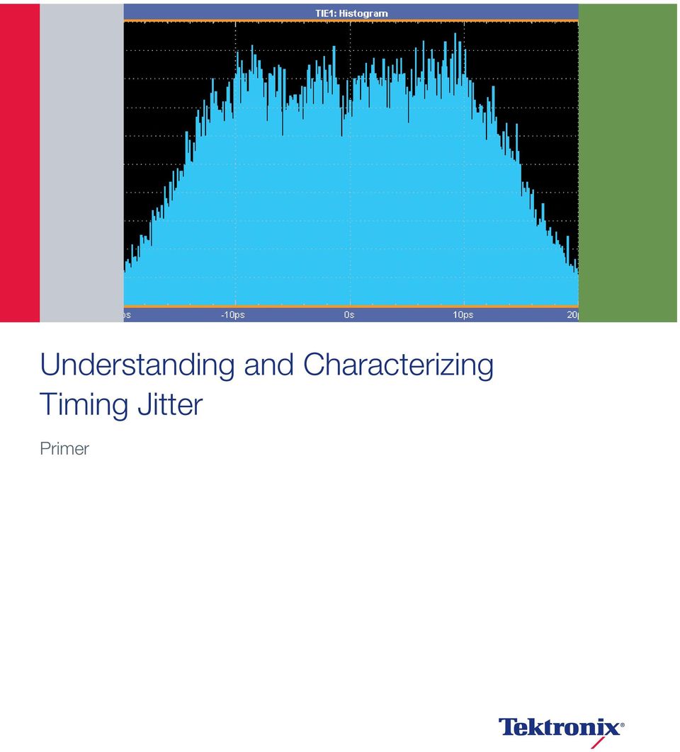
8 Primer Section 3: Jitter Measurement and Visualization The paragraphs in this section discuss some of the tools and techniques that are useful for quantifying and/or analyzing jitter. 3.1 Jitter Statistics Since all known signals contain jitter that has a random component, statistical measures are required to properly characterize the jitter. Some of the commonly used measures are: Mean Value: The arithmetic mean, or average, value of a clock period is the nominal period. This is the reciprocal of the frequency that a frequency counter would measure. The mean value of the TIE is theoretically zero, although a small residual value may result depending on the measurement technique. Standard Deviation: The standard deviation, represented by the greek character sigma (σ), is the average amount by which a measurement varies from its mean value. It is particularly useful in describing Gaussian processes, for which the distribution is completely specified by the mean and standard deviation. This is discussed at greater length in Section 4.3. Maximum, Minimum and Peak-Peak Values: The Max and Min values generally refer to values actually observed during a measurement interval, and the Peak-Peak value is simply the Max minus the Min. These measurements should be used judiciously. For a deterministic signal, these values may equal the true values even after a relatively short measurement interval. But for a random signal with a Gaussian distribution, there is theoretically no limit on the max and min values, so the observed peak-peak value will generally grow over time. For this reason, the peak-peak value should be used in conjunction with the population size and some knowledge of the type of distribution. Population: The population is the number of individual observations included in a statistical data set. For a random process, a high population intuitively gives greater confidence that the measurement results are repeatable. If the characteristics of the distribution are known or can be estimated, it is possible to calculate the population needed to reduce the measurement uncertainty below a desired point. HITS Figure 3.2a. Measurement Histogram. 3.2 Jitter Histogram VALUE A histogram is a diagram that plots the measurement values in a data set against the frequency of occurrence of the measurements. If the number of measurements in the data set is large, the histogram provides a good estimate of the probability density function (pdf) of the set. For example, if you rolled a fair die 1000 times and recorded the results, they might be as depicted in Figure 3.2a, where the HITS axis shows the number of times each value occurred. Note that a histogram provides no information about the order in which the observations occurred. An example of a jitter histogram for a TIE measurement is shown in Figure 3.2b. In this case, the continuous variable is mapped into 500 bins and the total population of the data set is 3,200,000. Since this is a TIE measurement, the mean value is 0 nsec. For this plot, the distribution is approximately Gaussian with a standard deviation of 1.3 psec. Consider a second example, in which the TIE of the signal in Figure 3.2b is modulated by the sine wave depicted in Figure 3.2c. 8

9 Understanding and Characterizing Timing Jitter Figure 3.2b. Histogram of a Time Interval Error Measurement. Figure 3.2c. Intended Sinewave Modulation to Apply to a Data Signal. 9

10 Primer Figure 3.2d. Time Interval Error of a Modulated Signal plotted as a Histogram. Figure 3.3a. Time Interval Error of a Modulated Signal plotted as a Trend. If this sine wave were sampled at an arbitrary instant, there is an equal likelihood that the sample value would lie anywhere between -15 nsec and 15 nsec. Hence, the TIE histogram of the modulated signal is spread over ±15 nsec with roughly equal likelihood, as shown in Figure 3.2d. (The steep but sloping tails at the left and right edges of the histogram show that the jitter still has a Gaussian component.) 3.3 Jitter vs. Time (Time Trend) Since the jitter histogram doesn t show the order in which the measurement observations occur, it cannot reveal repeating patterns that might indicate a modulation or other periodic component. A plot of jitter value versus time can make such a pattern obvious. As an example, the TIE from the phasemodulated signal of Figure 3.2d was plotted against time to produce Figure 3.3a. Now, the pattern of jitter variation becomes apparent, and its correlation with one of several possible sources of coupled noise might become clear. 10
 3.3 Jitter vs.")
11 Understanding and Characterizing Timing Jitter Figure 3.4a. Time Interval Error of a Modulated Signal plotted as a Spectrum. 3.4 Jitter vs. Frequency (Jitter Spectrum) Since the jitter measurements can be plotted versus time, an obvious extension is to apply a Fourier transform to these measurements and display the results in the frequency domain. This results in a jitter spectrum, with the modulation frequency displayed on the horizontal axis and the amplitude of modulation shown on the vertical axis. One of the benefits of spectral analysis is that periodic components that otherwise might be hidden by wideband noise can often be clearly distinguished. The prior example of a clock with sinusoidal modulation is used again here. Figure 3.4a shows the same TIE measurement as Figure 3.3a, displayed as a TIE spectrum. Now, the sinusoidal modulation is seen to have a fundamental frequency of 15 khz, as indicated by the largest spur. In theory, the Fourier series representation of a triangle wave only has odd harmonics. This is corroborated by the spectrum, where components can clearly be seen at 3 khz, 5 khz, 7 khz, and so on. The random noise still appears, but in this view it is manifested as a broad flat noise floor, that becomes flat above 2 MHz. It was mentioned earlier that timing variations with Fourier components below some limit, usually 10 Hz, are considered by convention to be wander rather than jitter. Of more practical interest, some other frequency limit (e.g. the loop bandwidth of your system s clock-recovery loop) may determine which noise can be safely tolerated. A spectral view of jitter can reveal whether the noise in a system is of concern or not. 11

12 Primer 3.5 Eye Diagram All of the methods discussed so far rely on edge locations only. These locations are extracted from a waveform by detecting when the waveform crosses one or more amplitude thresholds. The eye diagram is a more general tool, since it gives insight into the amplitude behavior of the waveform as well as the timing behavior. An eye diagram is created when many short segments of a waveform are superimposed such that the nominal edge locations and voltage levels are aligned, as suggested in Figure 3.5a. Usually, a horizontal span of two unit intervals is shown. The waveform segments may be adjacent ones, as shown in the figure, or may be taken from more widely spaced samples of the signal. If the waveform is repeatable, a sampling scope may be used to build an eye diagram from individual samples taken at random delays on many waveforms. Color has been used in the stylized Figure 3.5a to show how the individual waveform segments are composed into an eye diagram. In practice, eye diagrams are usually either monochrome or use color to indicate the density of waveform samples at any given point of the display. Figure 3.5b shows such a color density display for a waveform that exhibits several types of noise. In this diagram, white arrows are used to show the vertical and horizontal extent of the eye opening. As the noise on a signal increases, the eye becomes less open, either horizontally, vertically or both. The eye is said to be closed when no open area remains in the center of the diagram. The easiest way to create an eye diagram is with an oscilloscope in a long-persistence display mode. You should use caution in how you trigger the scope, if you use this approach. Simply triggering on a waveform edge will result in an eye diagram showing waveforms relative to that edge. This can be very different from an eye diagram relative to the underlying bit clock. To produce a diagram that is relative to the bit clock, you need some form of clock recovery, either in software or hardware. If your oscilloscope does not provide this feature, you may be able to use a trigger derived from an external clock-recovery circuit. The relationship between the eye diagram and the TIE histogram can be seen by turning the density eye diagram of Figure 3.5b into a three dimensional figure and slicing it along the decision threshold, as illustrated in Figure 3.5c. The area highlighted in pink is equivalent to a histogram of the first of the two zero-crossings in the eye diagram. Figure 3.5a. Constructing a Real-Time Eye Diagram. Figure 3.5b. A Waveform Database with Color Gradation. Figure 3.5c. In a Waveform Database, Colors can Represent Population. 12

13 Understanding and Characterizing Timing Jitter Figure 4.2. Jitter is Composed of Random and Deterministic Parts. Section 4: Jitter Separation All models are wrong; some models are useful - W. Edwards Deming Jitter separation, or jitter decomposition, is an analysis technique that uses a parameterized model to describe and predict system behavior. This section explains why this technique is used, and provides details about the jitter model most commonly used today. 4.1 Motivations for Decomposing Jitter To understand how real systems behave, it is often useful to use a mathematical model of the system. The behavior of such a model can be tuned by adjusting the parameters of its individual components. If the parameters of the model are chosen based on observations of the real system, then the model can be used to predict the behavior of the system in other situations. Thus, one of the motivations for jitter decomposition (also called jitter separation) is to extrapolate system performance to cases that would be difficult or timeconsuming to measure directly. Another motivation for modeling the system this way has to do with analysis. If each of the model components is associated with one or more underlying physical effects, an understanding of the model can provide insight into the precise cause or causes of excessive jitter. All models of complex systems make assumptions and simplifications, so the fit between the model and the true system behavior will never be exact. And in fact, there is usually some latitude in parameter choice when fitting the model s behavior to the observed measurements. For this reason, jitter separation has some elements of art as well as science, and "four nines" repeatability of measurements is not to be expected. Figure 4.2a. BUJ Values on BER Contour CDF. 4.2 The Jitter Model The jitter model which reflects the latest separation methods is based on the hierarchy shown in Figure 4.2. In this hierarchy, the total jitter (TJ) is first separated into two categories, random jitter (RJ) and deterministic jitter (DJ). It will be seen later that correctly distinguishing between these two jitter types has a dramatic impact on model correctness more so than any other modeling decision. The deterministic jitter is further subdivided into several categories: periodic jitter (PJ, also sometimes called sinusoidal jitter or SJ), duty-cycle dependent jitter (DCD), and data-dependent jitter (DDJ, also known as inter-symbol interference, ISI) and bounded, uncorrelated jitter (BUJ). See Figure 4.2a for an illustration of how BUJ values are displayed on a BERTScope BER Contour function. For each of these jitter types, the characteristics and root causes are discussed in the paragraphs that follow. 13

14 Primer Figure 4.2.1a. Gaussian Distribution Random Jitter Random jitter is timing noise that cannot be predicted, because it has no discernable pattern. A classic example of random noise is the sound that is heard when a radio receiver is tuned to an inactive carrier frequency. While a random process can, in theory, have any probability distribution, random jitter is assumed to have a Gaussian distribution for the purpose of the jitter model. One reason for this is that the primary source of random noise in many electrical circuits is thermal noise (also called Johnson noise or shot noise), which is known to have a Gaussian distribution. Another, more fundamental reason is that the composite effect of many uncorrelated noise sources, no matter what the distributions of the individual sources, approaches a Gaussian distribution according, to the central limit theorem. The Gaussian distribution, also known as the normal distribution, has a PDF that is described by the familiar bell curve. An example of the distribution, with a mean value of zero and a standard deviation of 1.0, is shown in Figure 4.2.1a. This distribution is covered thoroughly in one of the references in the bibliography 4, but its single most important characteristic is this: For a Gaussian variable, the peak value that it might attain is infinite. That is, although most samples of this random variable will be clustered around its mean value, any particular sample could, in theory, differ from that mean by an arbitrarily large amount. So, there is no bounded peak-topeak value for the underlying distribution. The more samples one takes of such a distribution, the larger the measured peak-to-peak value will be. Figure 4.2.1b. An Eye Diagram and Histogram of Gaussian Jitter. Frequently, efforts are made to characterize such a distribution by sampling it some large number of times and recording the peak-to-peak value that results. One should use caution with this approach. The peak-to-peak value of a set of N observations of a random variable is itself a random variable, albeit one with a lower standard deviation. Using such a random variable as a pass-fail criterion for quality screening, for example, requires that the pass threshold be raised to account for the uncertainty in the measurement, resulting in some acceptable units being failed. A better approach is to fit the N observations to the assumed distribution (in this case Gaussian). Then, the mathematical description of the distribution can be used to predict longer-term behavior to a particular confidence level. An eye diagram for a signal with only Gaussian jitter, together with the associated TIE histogram, is shown in Figure 4.2.1b. 14
, which is known to have a Gaussian distribution.")
15 Understanding and Characterizing Timing Jitter Figure 4.2.3a. A non-gaussian Distribution Deterministic Jitter Deterministic jitter is timing jitter that is repeatable and predictable. Because of this, the peak-to-peak value of this jitter is bounded, and the bounds can usually be observed or predicted with high confidence based on a reasonably low number of observations. This category of jitter is further subdivided in the paragraphs that follow, based both on the characteristics of the jitter and the root causes. Figure 4.2.3b. An Eye Diagram and Histogram of non-gaussian Jitter Periodic Jitter Jitter that repeats in a cyclic fashion is called periodic jitter. An example was shown in Figure 2.4c, where the TIE time trend shows a repeating triangle wave. Since any periodic waveform can be decomposed into a Fourier series of harmonically related sinusoids, this kind of jitter is sometimes called sinusoidal jitter. The probability distribution for a sine wave with peak amplitude of 1.0 is shown in Figure 4.2.3a. By convention, periodic jitter is uncorrelated with any periodically repeating patterns in a data stream. Jitter that is correlated with repeating data patterns is covered in the next paragraph. Periodic jitter is typically caused by external deterministic noise sources coupling into a system, such as switching powersupply noise or a strong local RF carrier. It may also be caused by an unstable clock-recovery PLL. An eye diagram for a signal with 0.2 unit intervals of periodic jitter, together with the associated TIE histogram, is shown in Figure 4.2.3b. 15

16 Primer Data-Dependent Jitter Any jitter that is correlated with the bit sequence in a data stream is termed Data-Dependent Jitter, or DDJ. DDJ is often caused by the frequency response of a cable or device. Consider the waveform in Figure 4.2.4a, in which a data sequence is strongly low-pass filtered. Because of the filtering, the waveform doesn t reach a full HIGH or LOW state unless there are several bits in a row of the same polarity. Figure 4.2.4b shows this waveform superimposed on an offset version of itself. You can see that an earlier threshold crossing occurs when a falling transition follows a 1,0,1,0,1,0,1 sequence than when following a 1,0,1,0,1,1,1 sequence. Since this timing shift is predictable and is related to the particular data preceding the transition, it is an example of DDJ. Another common name is Inter-Symbol Interference, or ISI. An eye diagram for a signal with 0.2 unit intervals of DDJ, together with the associated TIE histogram, is shown in Figure 4.2.4c. The histogram for ISI jitter always consists solely of impulses Duty-Cycle Dependent Jitter Jitter that may be predicted based on whether the associated edge is rising or falling is called Duty-Cycle Jitter (DCD). There are two common causes of DCD: 1. The slew rate for the rising edges differs from that of the falling edges. 2. The decision threshold for a waveform is higher or lower than it should be. Figure 4.2.5a is an eye diagram demonstrating the first case. Here, the decision threshold is at the 50% amplitude point but the slow rise time of the waveform causes the rising edges to cross the threshold later than the falling edges. As a result, the histogram of an edge crossing (gray) shows two distinct groupings. (In contrast to the prior eye diagrams, the waveform in this example has some Gaussian noise in addition to the duty-cycle jitter.) 0 Figure 4.2.4a. Data Signal with Data Dependent Jitter. 0 Figure 4.2.4b. Limited Bandpass One Source of Data Dependent Jitter. Figure 4.2.4c. An Eye Diagram and Histogram of Data Dependent Jitter. Figure 4.2.5a. Duty Cycle Distortion Caused by Non-symmetrical Rise/Fall Times. 16

17 Understanding and Characterizing Timing Jitter Figure 4.2.5b is an eye diagram showing the second case, in which the waveform has balanced rise and fall times but the decision threshold is not set at the 50% amplitude point. The edge-crossing histogram would look very much like that from Figure 4.2.5a Bounded, Uncorrelated Jitter (BUJ) Crosstalk between adjacent channels of high-speed interconnects like those found in 4 x 10GbE significantly affect the performance of serial links. Furthermore, the presence of crosstalk impairs the accuracy of traditional current jitter separation methodologies, resulting in reductions to the design margins for the high-speed link devices due to an overcalculation of random jitter. With a Bounded, Uncorrelated Jitter Component as part of jitter decomposition of signal impairments, the consequent BER eye synthesis leads to a more accurate evaluation. As shown in Figure 4.2.6, jitter results can be improved on high frequency serial links that appear in adjacent channel configurations. Figure 4.2.5b. Duty Cycle Distortion Caused by Incorrect Detection Threshold Subrate Jitter (SRJ) Often, Deterministic Jitter is induced into systems due to processing in nearby logic. Interactions like these cause jitter that could be synchronous or asynchronous and would fall into the category of BUJ ( Uncorrelated due to jitter not being correlated to the data pattern). Clock-synchronous jitter is a special and typical case of this type of jitter. Signal processing such as mux/demux, channel coding, block formatting and lower-speed parallel processing all have the potential of shifting edges at integer number of clock boundaries. A 4:1 mux stage on a transmitter as shown in Figure might advance or retard the timing of edges that occur at the same time as the internal divide-by-four clock parallel-loads all registers. If one were to look at four eye diagrams triggered by a one-quarter rate clock, they would see two eyes with the nominal eye width and one short and one long eye width surrounding the jittered edge. This would not be interpreted as ISI as it would be observed on all bits of the pattern (as long as the pattern length is not a multiple of four). Any non-harmonically related dissimilarity between the average transition times for all eyes that make up a given divide ratio is deterministic jitter that correlates to that divide ratio and is reported as Subrate Jitter (SRJ). Any BUJ that is larger than the SRJ number is further termed the Non-Subrate Jitter (NSR). Figure Improved TJ and greater margin using Bounded, Uncorrelated Jitter separation methodologies. Figure F/4 subrate jitter, where every 4th edge is late, causing uneven eye widths. Care must be taken to not confuse Subrate Jitter with pattern-dependent ISI. If the data pattern under test is a perfect multiple of a subrate divider, then the jitter found for that subrate is not included in the SRJ number as it will be correctly identified as a component of ISI. 17
 Crosstalk between adjacent channels of high-speed interconnects like those found in 4 x 10GbE significantly affect the performance of serial links.")
18 Primer DCD Jitter Distribution Composite Jitter Distribution Random Jitter Distribution Figure 4.3a. Random Jitter is Convolved with Deterministic Jitter to Find Total Jitter. 4.3 Putting It All Together The paragraphs above included eye diagrams and TIE histograms for each of the jitter types individually. But what happens to the histogram when more than one jitter type is present at the same time? A useful and applicable result from statistical theory can be paraphrased as follows: If two or more random processes are independent, the distribution that results from the sum of their effects is equal to the convolution of the individual distributions. A visual example of this concept is much more compelling than the verbal description. Figure 4.3a depicts what happens when duty-cycle jitter (with a histogram consisting of two impulses) is combined with random jitter (with its Gaussian distribution). Another example was shown earlier in Figure 3.2d, where the uniform distribution of a triangle wave (a form of periodic jitter) was combined with random jitter. A knowledgeable person could look at the final histogram from Figure 4.3a and infer what two types of jitter had contributed to it. However, real examples may involve all the jitter types in various amounts, resulting in a composite histogram that is much less intuitive. One of the objectives of a thorough jitter analysis is to identify all the individual jitter components that contributed to the final result. The real power of jitter separation comes when the accurately identified jitter components are inserted back into the jitter model outlined in Figure 4.2 and the model is used to predict how a system will behave in new circumstances. This is the basis for Bit Error Rate estimation, which is covered in more detail in Section 5. To understand why accurate analysis tools are important, we compare two systems with different jitter characteristics. The first system, identified as System I, has only random jitter with a standard deviation of unit intervals (UI). A TIE histogram for this system, which has a data rate of Mbps, is shown in Figure 4.3b. The second system has random jitter with a standard deviation of UI, about half that of the first system. However, it also has two uncorrelated components of periodic jitter, each with a peak-to-peak amplitude of 0.14 UI. Figure 4.3c shows the TIE histogram for System II. The two histograms, which contain identical populations of about 42,000 edges, don t look remarkably different. In fact, for these two sample sets the peak-to-peak value of the time interval error is exactly the same: 430 ps (0.457 UI). If visual comparison were the only tool available, distinguishing between these two cases would be difficult. Accurately predicting how the systems might behave over a longer observation interval would be impossible. One might ask whether it is important to distinguish between these cases, since they look so similar. We shall return for a second look at this example after a review of Bit Error Rates and Bathtub curves. 18

19 Understanding and Characterizing Timing Jitter Figure 4.3b. A Histogram of a Jitter Distribution with Dominant Random Jitter. Figure 4.3c. A Histogram of a Jitter Distribution with Dominant Deterministic Jitter. 19

20 Primer Transmitter Channel Receiver Serial Data Source Connector Cable Connector Amplifier Clock Data Recovery (CDR) A B Access Points C D Figure 5.1. Common Measurement Points for Setting System Jitter Budgets. Section 5: Jitter vs. Bit Error Rate An approximate answer to the right question is worth a good deal more than the exact answer to an approximate problem. - John Tukey 5.1 The Jitter Budget A real communications system consists of transmitter, channel and receiver, as modeled in Figure 5.1. The channel may include cabling, interconnects, and active devices that don t perform clock regeneration. The channel may introduce filtering, non-linearity, DC offset, impedance mismatches and additional random jitter. Various circuit test points and system connectors will provide access points where the signal quality may be monitored. As one progresses from the transmitter to the receiver and monitors the signal quality at each access point (perhaps using an eye diagram), the signal jitter generally gets worse. Simplistically, one might assume that success has been achieved if the eye is still open, even just a little, when the signal reaches the input to the receiver s clock-data recovery circuit (access point D). However, the receiver circuit isn t perfect. The received signal s eye must be sufficiently open horizontally to account for timing uncertainty in the receiver s decision circuit, and open enough vertically to accommodate noise influencing the decision threshold. Thus, a thorough system design specification will allocate a jitter budget so that each well-defined access point has known jitter limits, and that adequate margin remains when the signal enters the receiver to be resynchronized. 20

21 Understanding and Characterizing Timing Jitter Figure 5.2a. Eye Width is used to Determine Performance. Figure 5.2b. Measuring Eye Width Over Time to Determine Bit Error Ratio. Now suppose instead that the test was considered successful if no more than one waveform out of every 1000 waveforms crossed over the ruler. It would no longer matter how long the test ran. If 50,000 waveforms were allowed to accumulate and 50 or less crossed over the ruler, the test would have passed. One could say that, aside from one waveform in 10 3, the eye was 50% open. Since each crossing is assumed to represent a bit error, this would be a bit error rate (BER) of If the same signal were tested with a shorter ruler, say, 0.25 unit intervals long, then the ruler would certainly be crossed less frequently. Perhaps only one waveform out of every 100,000 waveforms, on average, would cross this shorter ruler. One could say that, aside from one waveform in 10 5, the eye was 25% open. Figure 5.2c. BER Contour Plot with specific BER performance on traditional eye pattern. 5.2 The Bathtub Curve The concepts of eye diagrams and eye openings were discussed in Section 3.5. The Gaussian probability distribution, with its theoretically unbounded peak-to-peak value, was covered in paragraph Considering these two topics together leads to an interesting thought: For any signal that contains some Gaussian jitter, the eye diagram should close completely if you accumulate samples for a long enough time. This would render the concept of eye opening useless as a basis for comparison. Fortunately, the usefulness of the eye diagram is restored if a confidence level is applied to the eye opening. Consider Figure 5.2a, in which a green ruler 0.5 unit intervals long has been placed horizontally in the center of the eye. Suppose that it is regarded a failure if any waveforms cross this ruler, either rising or falling. In the figure, it appears that this ruler has not been crossed by any waveforms yet, but such a crossing is inevitable if waveform samples continue to accumulate and the signal contains some Gaussian jitter. Continuing along these lines and using a series of rulers, one could fully characterize the eye opening versus the bit error rate. (Note that each ruler should be allowed to slide left or right to obtain the best possible fit.) If the rulers are all plotted against their corresponding bit error rates on a single chart, with the ends of the rulers connected, a plot something like Figure 5.2b results. A plot of this description is called a Bathtub Plot, since the pink lines can be imagined to look like a bathtub. Using such a figure, one can tell what horizontal portion of the eye will remain completely free of signal transitions, for a given confidence level. Finally, note that it can take a long time to accumulate enough data to directly measure the eye openings near the bottom of the chart. For this reason, the mathematical model covered in Section 4 can be used to predict performance on the basis of a much smaller sample set. Another concept that is helpful for identifying jitter performance at a specific BER level is the BER contour plot. A BER contour (Figure 5.2c) is a two dimensional extension of the bathtub plot, and can be measured radially around the eye opening to provide a visual representation of the eye opening at specific BER levels. 21
22 Primer Figure 5.3a. BER Plot of System with Dominant Random Jitter. Figure 5.3b. BER Plot of System with Dominant Deterministic Jitter. 5.3 A BER Example Section 4.3 presented an example in which two systems with different jitter characteristics had similar TIE histograms and identical peak-to-peak jitter for a sample size of about 42,000 edges. (See Figures 4.3b and 4.3c.) We now return to that example, and show the associated bathtub curves. Figure 5.3a shows the bathtub curve for System I, and Figure 5.3b shows the plot for System II. Since both of these plots represent data sets of 42,000 observed edges, a red cursor has been placed on each plot corresponding to a BER of one part in 42,000, or At these levels, both of the systems show an eye opening of about 58%, and the eye opening for System I is actually greater than that for System II. However, at a BER of 1e-12 (which is a frequent specification point for serial communication links) the eye for System I is only open 26%. The eye for System II is open 37%, or about half-again as much as System I. This is a significant difference, and could easily determine whether a system meets its requirements or not. 22
23 Understanding and Characterizing Timing Jitter Section 6: Summary Timing jitter has always degraded electrical systems, but the drive to higher data rates and lower logic swings has focused increasing interest and concern on its characterization. Characterization is needed to identify sources of jitter for reduction by redesign. It also serves to define, identify or measure jitter for compliance standards and design specifications. All jitter has random and deterministic components. Because of its random nature, care must be used in specifying acceptable limits for jitter. This is especially true when jitter performance at very high confidence levels is to be estimated based on modest amounts of data. To enable working with random components of jitter, a method that has found favor in jitter analysis and prediction is to use a mathematical model, the parameters of which are adjusted based on observed measurements. The model can then be used to predict performance in other situations. The model can also give insight into the specific causes of the jitter, and therefore aid in understanding how to reduce it. The oscilloscope has been a traditional tool for observing jitter, using such techniques as histograms and eye diagrams. When augmented by back-end processing that provides additional features like cycle to cycle measurements, trend and spectrum plots, data logging and worst case capture, the scope continues to be the tool of choice for characterizing timing jitter. When further augmented with sophisticated clock recovery, jitter separation algorithms and bit error ratio estimation, the scope becomes the only solution for characterizing and reducing timing jitter. Many of the figures and examples in this document were taken from the Tektronix DPOJET Jitter and Eye Diagram Analysis Tools, which runs on Tektronix MSO/DPO Series oscilloscopes and the Tektronix BERTScope Bit Error Rate Tester, which is capable of making actual BER measurements at the 10 e-12 level, providing a high confidence measurement of TJ. Also shown in the examples were the BERTScope's ability to measure TJ on individual bits in a pattern, enalbing a new means for jitter separation in a BER tester. Appendix A: Glossary of Acronyms BER Bit Error Rate BUJ Bounded, Uncorrelated Jitter CDF Cumulative Distribution Function DCD Duty-Cycle Jitter DDJ Data-Dependent Jitter DJ FFT ISI Deterministic Jitter Fast Fourier Transform Inter-Symbol Interference PDF Probability Density Function PJ Periodic Jitter PLL Phase-Locked Loop PSD Power Spectral Density RJ SJ Random Jitter Sinusoidal Jitter SRJ Subrate Jitter TIE TJ UI Time Interval Error Total Jitter Unit Interval References 1 Bell Communications Research, Inc (Bellcore), Synchrouous Optical Network (SONET) Transport Systems: Common Generic Criteria, TR-253-CORE, Issue 2, Rev No. 1, December ITU-T Recommendation G.810 (08/96) Definitions and Terminology for Synchronization Networks 3 Papoulis: Probability, Random Variables, and Stochastic Processes, Second Edition, McGraw-Hill, Davenport and Root: An Introduction to the Theory of Random Signals and Noise, IEEE Press,
24 Contact Tektronix: ASEAN / Australasia (65) Austria* Balkans, Israel, South Africa and other ISE Countries Belgium* Brazil +55 (11) Canada 1 (800) Central East Europe and the Baltics Central Europe & Greece Denmark Finland France* Germany* Hong Kong India Italy* Japan 81 (3) Luxembourg Mexico, Central/South America & Caribbean 52 (55) Middle East, Asia and North Africa The Netherlands* Norway People s Republic of China Poland Portugal Republic of Korea Russia & CIS +7 (495) South Africa Spain* Sweden* Switzerland* Taiwan 886 (2) United Kingdom & Ireland* USA 1 (800) * If the European phone number above is not accessible, please call Contact List Updated 10 February 2011 For Further Information Tektronix maintains a comprehensive, constantly expanding collection of application notes, technical briefs and other resources to help engineers working on the cutting edge of technology. Please visit Copyright 2012, Tektronix. All rights reserved. Tektronix products are covered by U.S. and foreign patents, issued and pending. Information in this publication supersedes that in all previously published material. Specification and price change privileges reserved. TEKTRONIX and TEK are registered trademarks of Tektronix, Inc. All other trade names referenced are the service marks, trademarks or registered trademarks of their respective companies. 09/12 EA/WWW 55W
How To Understand And Understand Jitter On A Network Device
 Understanding and Characterizing Timing Jitter Table of Contents Introduction... 3 Section 1: The Consequences of Jitter... 3 Computer Bus Design 3 Serial Data Link 4 Section 2: Just What is Jitter?...
Time-Correlated Multi-domain RF Analysis with the MSO70000 Series Oscilloscope and SignalVu Software
 Time-Correlated Multi-domain RF Analysis with the MSO70000 Series Oscilloscope and SignalVu Software Technical Brief Introduction The MSO70000 Series Mixed Oscilloscope, when coupled with SignalVu Spectrum
High-Speed Inter Connect (HSIC) Solution
 Solution") High-Speed Inter Connect (HSIC) Solution HSIC Essentials Datasheet Protocol Decode Protocol decode Saves test time and resource costs. Designed for use with the MSO/DPO5000, DPO7000C, DPO/DSA/MSO70000C,
High-Speed Inter Connect (HSIC) Solution HSIC Essentials Datasheet Protocol Decode Protocol decode Saves test time and resource costs. Designed for use with the MSO/DPO5000, DPO7000C, DPO/DSA/MSO70000C,
TDS5000B, TDS6000B, TDS/CSA7000B Series Acquisition Modes
 TDS5000B, TDS6000B, TDS/CSA7000B Series Acquisition Modes Tektronix oscilloscopes provide several different acquisition modes. While this gives the user great flexibility and choice, each mode is optimized
TekConnect Adapters. TCA75 TCA-BNC TCA-SMA TCA-N TCA-292MM Data Sheet. Applications. Features & Benefits
 TekConnect Adapters TCA75 TCA-BNC TCA-SMA TCA-N TCA-292MM Data Sheet TCA-N TekConnect-to-N DC to 11 GHz (Instrument Dependent) 50 Ω Input (Only) TCA-SMA TekConnect-to-SMA DC to 18 GHz (Instrument Dependent)
Jitter Measurements in Serial Data Signals
 Jitter Measurements in Serial Data Signals Michael Schnecker, Product Manager LeCroy Corporation Introduction The increasing speed of serial data transmission systems places greater importance on measuring
PCI Express Transmitter PLL Testing A Comparison of Methods. Primer
 PCI Express Transmitter PLL Testing A Comparison of Methods Primer Primer Table of Contents Abstract...3 Spectrum Analyzer Method...4 Oscilloscope Method...6 Bit Error Rate Tester (BERT) Method...6 Clock
Timing Errors and Jitter
 Timing Errors and Jitter Background Mike Story In a sampled (digital) system, samples have to be accurate in level and time. The digital system uses the two bits of information the signal was this big
Physical Layer Compliance Testing for 100BASE-TX
 Physical Layer Compliance Testing for 100BASE-TX Application Note Engineers designing or validating the Ethernet physical layer on their products need to perform a wide range of tests, quickly, reliably
Clock Recovery Primer, Part 1. Primer
 Clock Recovery Primer, Part 1 Primer Primer Table of Contents Abstract...3 Why is Clock Recovery Used?...3 How Does Clock Recovery Work?...3 PLL-Based Clock Recovery...4 Generic Phased Lock Loop Block
Advanced Power Measurement and Analysis Software DPOPWR Datasheet
 Advanced Power Measurement and Analysis Software DPOPWR Datasheet Power quality measurements computes THD, True Power, Apparent Power, Power Factor, and Crest Factor. These analysis outputs are shown in
What is the difference between an equivalent time sampling oscilloscope and a real-time oscilloscope?
 What is the difference between an equivalent time sampling oscilloscope and a real-time oscilloscope? Application Note In the past, deciding between an equivalent time sampling oscilloscope and a real
Clock Jitter Definitions and Measurement Methods
 January 2014 Clock Jitter Definitions and Measurement Methods 1 Introduction Jitter is the timing variations of a set of signal edges from their ideal values. Jitters in clock signals are typically caused
Clock Recovery in Serial-Data Systems Ransom Stephens, Ph.D.
 Clock Recovery in Serial-Data Systems Ransom Stephens, Ph.D. Abstract: The definition of a bit period, or unit interval, is much more complicated than it looks. If it were just the reciprocal of the data
High-voltage Differential Probes TMDP0200 - THDP0200 - THDP0100 - P5200A - P5202A - P5205A - P5210A
 High-voltage Differential Probes TMDP0200 - THDP0200 - THDP0100 - P5200A - P5202A - P5205A - P5210A BNC interface (P5200A probes) TekVPI interface (TMDP and THDP Series probes) TekProbe interface (P5202A,
Evaluating Oscilloscope Bandwidths for Your Application
 Evaluating Oscilloscope Bandwidths for Your Application Application Note Table of Contents Introduction....1 Defining Oscilloscope Bandwidth.....2 Required Bandwidth for Digital Applications...4 Digital
1.5 GHz Active Probe TAP1500 Datasheet
 1.5 GHz Active Probe TAP1500 Datasheet Easy to use Connects directly to oscilloscopes with the TekVPI probe interface Provides automatic units scaling and readout on the oscilloscope display Easy access
Loop Bandwidth and Clock Data Recovery (CDR) in Oscilloscope Measurements. Application Note 1304-6
 in Oscilloscope Measurements. Application Note 1304-6") Loop Bandwidth and Clock Data Recovery (CDR) in Oscilloscope Measurements Application Note 1304-6 Abstract Time domain measurements are only as accurate as the trigger signal used to acquire them. Often
Loop Bandwidth and Clock Data Recovery (CDR) in Oscilloscope Measurements Application Note 1304-6 Abstract Time domain measurements are only as accurate as the trigger signal used to acquire them. Often
Q Factor: The Wrong Answer for Service Providers and NEMs White Paper
 Q Factor: The Wrong Answer for Service Providers and NEMs White Paper By Keith Willox Business Development Engineer Transmission Test Group Agilent Technologies Current market conditions throughout the
ANALYZER BASICS WHAT IS AN FFT SPECTRUM ANALYZER? 2-1
 WHAT IS AN FFT SPECTRUM ANALYZER? ANALYZER BASICS The SR760 FFT Spectrum Analyzer takes a time varying input signal, like you would see on an oscilloscope trace, and computes its frequency spectrum. Fourier's
How to Measure 5 ns Rise/Fall Time on an RF Pulsed Power Amplifier Using the 8990B Peak Power Analyzer
 How to Measure 5 ns Rise/Fall Time on an RF Pulsed Power Amplifier Using the 8990B Peak Power Analyzer Application Note Introduction In a pulsed radar system, one of the key transmitter-side components
Department of Electrical and Computer Engineering Ben-Gurion University of the Negev. LAB 1 - Introduction to USRP
 Department of Electrical and Computer Engineering Ben-Gurion University of the Negev LAB 1 - Introduction to USRP - 1-1 Introduction In this lab you will use software reconfigurable RF hardware from National
RF Measurements Using a Modular Digitizer
 RF Measurements Using a Modular Digitizer Modern modular digitizers, like the Spectrum M4i series PCIe digitizers, offer greater bandwidth and higher resolution at any given bandwidth than ever before.
Highly Reliable Testing of 10-Gb/s Systems (STM-64/OC-192)
") Highly Reliable Testing of 10-Gb/s Systems (STM-64/OC-192) Meeting the Growing Need for Bandwidth The communications industry s insatiable need for bandwidth, driven primarily by the exploding growth in
Highly Reliable Testing of 10-Gb/s Systems (STM-64/OC-192) Meeting the Growing Need for Bandwidth The communications industry s insatiable need for bandwidth, driven primarily by the exploding growth in
Testing Video Transport Streams Using Templates
 Testing Video Transport Streams Using Templates Using Templates to Ensure Transport Stream Performance As the number of digital television services being distributed around the world increases, the need
802.11ac Power Measurement and Timing Analysis
 802.11ac Power Measurement and Timing Analysis Using the 8990B Peak Power Analyzer Application Note Introduction There are a number of challenges to anticipate when testing WLAN 802.11ac [1] power amplifier
Selecting RJ Bandwidth in EZJIT Plus Software
 Selecting RJ Bandwidth in EZJIT Plus Software Application Note 1577 Introduction Separating jitter into its random and deterministic components (called RJ/DJ separation ) is a relatively new technique
USB 3.0 CDR Model White Paper Revision 0.5
 USB 3.0 CDR Model White Paper Revision 0.5 January 15, 2009 INTELLECTUAL PROPERTY DISCLAIMER THIS WHITE PAPER IS PROVIDED TO YOU AS IS WITH NO WARRANTIES WHATSOEVER, INCLUDING ANY WARRANTY OF MERCHANTABILITY,
How To Use A High Definition Oscilloscope
 PRELIMINARY High Definition Oscilloscopes HDO4000 and HDO6000 Key Features 12-bit ADC resolution, up to 15-bit with enhanced resolution 200 MHz, 350 MHz, 500 MHz, 1 GHz bandwidths Long Memory up to 250
TekSmartLab TBX3000A, TSL3000B Datasheet
 TekSmartLab TBX3000A, TSL3000B Datasheet TekSmartLab is the industry's first network-based instrument management solution for teaching labs that brings a more efficient lab experience. With the TekSmartLab,
T = 1 f. Phase. Measure of relative position in time within a single period of a signal For a periodic signal f(t), phase is fractional part t p
, phase is fractional part t p") Data Transmission Concepts and terminology Transmission terminology Transmission from transmitter to receiver goes over some transmission medium using electromagnetic waves Guided media. Waves are guided
Data Transmission Concepts and terminology Transmission terminology Transmission from transmitter to receiver goes over some transmission medium using electromagnetic waves Guided media. Waves are guided
Jitter in PCIe application on embedded boards with PLL Zero delay Clock buffer
 Jitter in PCIe application on embedded boards with PLL Zero delay Clock buffer Hermann Ruckerbauer EKH - EyeKnowHow 94469 Deggendorf, Germany Hermann.Ruckerbauer@EyeKnowHow.de Agenda 1) PCI-Express Clocking
AN-837 APPLICATION NOTE
 APPLICATION NOTE One Technology Way P.O. Box 916 Norwood, MA 262-916, U.S.A. Tel: 781.329.47 Fax: 781.461.3113 www.analog.com DDS-Based Clock Jitter Performance vs. DAC Reconstruction Filter Performance
Make Better RMS Measurements with Your DMM
 Make Better RMS Measurements with Your DMM Application Note Introduction If you use a digital multimeter (DMM) for AC voltage measurements, it is important to know if your meter is giving you peak value,
The Fundamentals of Three-Phase Power Measurements. Application Note
 The Fundamentals of - Power Measurements pplication ote pplication ote 0 120 240 360 Figure 1. -phase voltage wavefm. Figure 2. -phase voltage vects. 100Ω 100Ω Figure 4. -phase supply, balanced load -
MODULATION Systems (part 1)
") Technologies and Services on Digital Broadcasting (8) MODULATION Systems (part ) "Technologies and Services of Digital Broadcasting" (in Japanese, ISBN4-339-62-2) is published by CORONA publishing co.,
Technologies and Services on Digital Broadcasting (8) MODULATION Systems (part ) "Technologies and Services of Digital Broadcasting" (in Japanese, ISBN4-339-62-2) is published by CORONA publishing co.,
Implementation of Digital Signal Processing: Some Background on GFSK Modulation
 Implementation of Digital Signal Processing: Some Background on GFSK Modulation Sabih H. Gerez University of Twente, Department of Electrical Engineering s.h.gerez@utwente.nl Version 4 (February 7, 2013)
The Effect of Network Cabling on Bit Error Rate Performance. By Paul Kish NORDX/CDT
 The Effect of Network Cabling on Bit Error Rate Performance By Paul Kish NORDX/CDT Table of Contents Introduction... 2 Probability of Causing Errors... 3 Noise Sources Contributing to Errors... 4 Bit Error
EXPERIMENT NUMBER 5 BASIC OSCILLOSCOPE OPERATIONS
 1 EXPERIMENT NUMBER 5 BASIC OSCILLOSCOPE OPERATIONS The oscilloscope is the most versatile and most important tool in this lab and is probably the best tool an electrical engineer uses. This outline guides
Making Accurate Voltage Noise and Current Noise Measurements on Operational Amplifiers Down to 0.1Hz
 Author: Don LaFontaine Making Accurate Voltage Noise and Current Noise Measurements on Operational Amplifiers Down to 0.1Hz Abstract Making accurate voltage and current noise measurements on op amps in
Electronic Communications Committee (ECC) within the European Conference of Postal and Telecommunications Administrations (CEPT)
 within the European Conference of Postal and Telecommunications Administrations (CEPT)") Page 1 Electronic Communications Committee (ECC) within the European Conference of Postal and Telecommunications Administrations (CEPT) ECC RECOMMENDATION (06)01 Bandwidth measurements using FFT techniques
Page 1 Electronic Communications Committee (ECC) within the European Conference of Postal and Telecommunications Administrations (CEPT) ECC RECOMMENDATION (06)01 Bandwidth measurements using FFT techniques
NRZ Bandwidth - HF Cutoff vs. SNR
 Application Note: HFAN-09.0. Rev.2; 04/08 NRZ Bandwidth - HF Cutoff vs. SNR Functional Diagrams Pin Configurations appear at end of data sheet. Functional Diagrams continued at end of data sheet. UCSP
Rapid Resolution of Trouble Tickets
 Rapid Resolution of Trouble Tickets How to solve trouble-tickets faster with the new K15 Iub monitoring/automatic configuration and UMTS Multi Interface Call Trace applications Trouble ticket. It is an
Pericom PCI Express 1.0 & PCI Express 2.0 Advanced Clock Solutions
 Pericom PCI Express 1.0 & PCI Express 2.0 Advanced Clock Solutions PCI Express Bus In Today s Market PCI Express, or PCIe, is a relatively new serial pointto-point bus in PCs. It was introduced as an AGP
Agilent BenchVue Software (34840B) Data capture simplified. Click, capture, done. Data Sheet
 Data capture simplified. Click, capture, done. Data Sheet") Agilent BenchVue Software (34840B) Data capture simplified. Click, capture, done. Data Sheet Use BenchVue software to: Visualize multiple measurements simultaneously Easily capture data, screen shots and
Agilent BenchVue Software (34840B) Data capture simplified. Click, capture, done. Data Sheet Use BenchVue software to: Visualize multiple measurements simultaneously Easily capture data, screen shots and
SIGNAL GENERATORS and OSCILLOSCOPE CALIBRATION
 1 SIGNAL GENERATORS and OSCILLOSCOPE CALIBRATION By Lannes S. Purnell FLUKE CORPORATION 2 This paper shows how standard signal generators can be used as leveled sine wave sources for calibrating oscilloscopes.
Non-Data Aided Carrier Offset Compensation for SDR Implementation
 Non-Data Aided Carrier Offset Compensation for SDR Implementation Anders Riis Jensen 1, Niels Terp Kjeldgaard Jørgensen 1 Kim Laugesen 1, Yannick Le Moullec 1,2 1 Department of Electronic Systems, 2 Center
CLOCK AND SYNCHRONIZATION IN SYSTEM 6000
 By Christian G. Frandsen Introduction This document will discuss the clock, synchronization and interface design of TC System 6000 and deal with several of the factors that must be considered when using
Clock Recovery Primer, Part 2. Primer
 Clock Recovery Primer, Part 2 Primer Primer Table of Contents Abstract...3 9. Loop Types and Orders...3 Notes on Type II Loops [1]...3 Example SOTII Transfer Function...3 Notes on Type I Loops [1]...3
Optimizing VCO PLL Evaluations & PLL Synthesizer Designs
 Optimizing VCO PLL Evaluations & PLL Synthesizer Designs Today s mobile communications systems demand higher communication quality, higher data rates, higher operation, and more channels per unit bandwidth.
GigaSPEED X10D Solution How
 SYSTIMAX Solutions GigaSPEED X10D Solution How White Paper June 2009 www.commscope.com Contents Modal Decomposition Modeling and the Revolutionary 1 SYSTIMAX GigaSPEED X10D Performance MDM An Introduction
Explore Efficient Test Approaches for PCIe at 16GT/s Kalev Sepp Principal Engineer Tektronix, Inc
 Explore Efficient Test Approaches for PCIe at 16GT/s Kalev Sepp Principal Engineer Tektronix, Inc Copyright 2015, PCI-SIG, All Rights Reserved 1 Disclaimer Presentation Disclaimer: All opinions, judgments,
Evaluating Oscilloscope Sample Rates vs. Sampling Fidelity
 Evaluating Oscilloscope Sample Rates vs. Sampling Fidelity Application Note How to Make the Most Accurate Digital Measurements Introduction Digital storage oscilloscopes (DSO) are the primary tools used
The Effective Number of Bits (ENOB) of my R&S Digital Oscilloscope Technical Paper
 of my R&S Digital Oscilloscope Technical Paper") The Effective Number of Bits (ENOB) of my R&S Digital Oscilloscope Technical Paper Products: R&S RTO1012 R&S RTO1014 R&S RTO1022 R&S RTO1024 This technical paper provides an introduction to the signal
The Effective Number of Bits (ENOB) of my R&S Digital Oscilloscope Technical Paper Products: R&S RTO1012 R&S RTO1014 R&S RTO1022 R&S RTO1024 This technical paper provides an introduction to the signal
Agilent Creating Multi-tone Signals With the N7509A Waveform Generation Toolbox. Application Note
 Agilent Creating Multi-tone Signals With the N7509A Waveform Generation Toolbox Application Note Introduction Of all the signal engines in the N7509A, the most complex is the multi-tone engine. This application
Introduction to Digital Audio
 Introduction to Digital Audio Before the development of high-speed, low-cost digital computers and analog-to-digital conversion circuits, all recording and manipulation of sound was done using analog techniques.
Taking the Mystery out of the Infamous Formula, "SNR = 6.02N + 1.76dB," and Why You Should Care. by Walt Kester
 ITRODUCTIO Taking the Mystery out of the Infamous Formula, "SR = 6.0 + 1.76dB," and Why You Should Care by Walt Kester MT-001 TUTORIAL You don't have to deal with ADCs or DACs for long before running across
Jitter Transfer Functions in Minutes
 Jitter Transfer Functions in Minutes In this paper, we use the SV1C Personalized SerDes Tester to rapidly develop and execute PLL Jitter transfer function measurements. We leverage the integrated nature
PCI-SIG ENGINEERING CHANGE NOTICE
 PCI-SIG ENGINEERING CHANGE NOTICE TITLE: Separate Refclk Independent SSC Architecture (SRIS) DATE: Updated 10 January 013 AFFECTED DOCUMENT: PCI Express Base Spec. Rev. 3.0 SPONSOR: Intel, HP, AMD Part
DDR Memory Overview, Development Cycle, and Challenges
 DDR Memory Overview, Development Cycle, and Challenges Tutorial DDR Overview Memory is everywhere not just in servers, workstations and desktops, but also embedded in consumer electronics, automobiles
Agilent MATLAB Data Analysis Software Packages for Agilent Oscilloscopes
 Agilent MATLAB Data Analysis Software Packages for Agilent Oscilloscopes Data Sheet Enhance your InfiniiVision or Infiniium oscilloscope with the analysis power of MATLAB software Develop custom analysis
The Fourier Analysis Tool in Microsoft Excel
 The Fourier Analysis Tool in Microsoft Excel Douglas A. Kerr Issue March 4, 2009 ABSTRACT AD ITRODUCTIO The spreadsheet application Microsoft Excel includes a tool that will calculate the discrete Fourier
Reading: HH Sections 4.11 4.13, 4.19 4.20 (pgs. 189-212, 222 224)
") 6 OP AMPS II 6 Op Amps II In the previous lab, you explored several applications of op amps. In this exercise, you will look at some of their limitations. You will also examine the op amp integrator and
6 OP AMPS II 6 Op Amps II In the previous lab, you explored several applications of op amps. In this exercise, you will look at some of their limitations. You will also examine the op amp integrator and
Successfully negotiating the PCI EXPRESS 2.0 Super Highway Towards Full Compliance
 Successfully negotiating the PCI EXPRESS 2.0 Super Highway Towards Full Compliance Page 1 Agenda Introduction PCIe 2.0 changes from 1.0a/1.1 Spec 5GT/s Challenges Error Correction Techniques Test tool
Application Note Noise Frequently Asked Questions
 : What is? is a random signal inherent in all physical components. It directly limits the detection and processing of all information. The common form of noise is white Gaussian due to the many random
Computer Networks and Internets, 5e Chapter 6 Information Sources and Signals. Introduction
 Computer Networks and Internets, 5e Chapter 6 Information Sources and Signals Modified from the lecture slides of Lami Kaya (LKaya@ieee.org) for use CECS 474, Fall 2008. 2009 Pearson Education Inc., Upper
Agilent AN 1316 Optimizing Spectrum Analyzer Amplitude Accuracy
 Agilent AN 1316 Optimizing Spectrum Analyzer Amplitude Accuracy Application Note RF & Microwave Spectrum Analyzers Table of Contents 3 3 4 4 5 7 8 8 13 13 14 16 16 Introduction Absolute versus relative
Signal Types and Terminations
 Helping Customers Innovate, Improve & Grow Application Note Signal Types and Terminations Introduction., H, LV, Sinewave, Clipped Sinewave, TTL, PECL,,, CML Oscillators and frequency control devices come
PCM Encoding and Decoding:
 PCM Encoding and Decoding: Aim: Introduction to PCM encoding and decoding. Introduction: PCM Encoding: The input to the PCM ENCODER module is an analog message. This must be constrained to a defined bandwidth
Impedance 50 (75 connectors via adapters)
") VECTOR NETWORK ANALYZER PLANAR TR1300/1 DATA SHEET Frequency range: 300 khz to 1.3 GHz Measured parameters: S11, S21 Dynamic range of transmission measurement magnitude: 130 db Measurement time per point:
VECTOR NETWORK ANALYZER PLANAR TR1300/1 DATA SHEET Frequency range: 300 khz to 1.3 GHz Measured parameters: S11, S21 Dynamic range of transmission measurement magnitude: 130 db Measurement time per point:
11. High-Speed Differential Interfaces in Cyclone II Devices
 11. High-Speed Differential Interfaces in Cyclone II Devices CII51011-2.2 Introduction From high-speed backplane applications to high-end switch boxes, low-voltage differential signaling (LVDS) is the
Understand the effects of clock jitter and phase noise on sampled systems A s higher resolution data converters that can
 designfeature By Brad Brannon, Analog Devices Inc MUCH OF YOUR SYSTEM S PERFORMANCE DEPENDS ON JITTER SPECIFICATIONS, SO CAREFUL ASSESSMENT IS CRITICAL. Understand the effects of clock jitter and phase
Agilent U2000 Series USB Power Sensors
 Agilent U2000 Series USB Power Sensors GSM Timeslot Burst Power Measurement Product Note Table of Content Introduction 2 Measuring GSM Timeslot 4 Signal Overview of Agilent U2000 5 Series USB Power Sensors
isim ACTIVE FILTER DESIGNER NEW, VERY CAPABLE, MULTI-STAGE ACTIVE FILTER DESIGN TOOL
 isim ACTIVE FILTER DESIGNER NEW, VERY CAPABLE, MULTI-STAGE ACTIVE FILTER DESIGN TOOL Michael Steffes Sr. Applications Manager 12/15/2010 SIMPLY SMARTER Introduction to the New Active Filter Designer Scope
DSAM Digital Quality Index (DQI) A New Technique for Assessing Downstream Digital Services
 A New Technique for Assessing Downstream Digital Services") Application Note DSAM Digital Quality Index (DQI) A New Technique for Assessing Downstream Digital Services Overview As cable operators move to digital simulcast and all digital networks, the majority
Application Note DSAM Digital Quality Index (DQI) A New Technique for Assessing Downstream Digital Services Overview As cable operators move to digital simulcast and all digital networks, the majority
GETTING STARTED WITH LABVIEW POINT-BY-POINT VIS
 USER GUIDE GETTING STARTED WITH LABVIEW POINT-BY-POINT VIS Contents Using the LabVIEW Point-By-Point VI Libraries... 2 Initializing Point-By-Point VIs... 3 Frequently Asked Questions... 5 What Are the
Optimizing IP3 and ACPR Measurements
 Optimizing IP3 and ACPR Measurements Table of Contents 1. Overview... 2 2. Theory of Intermodulation Distortion... 2 3. Optimizing IP3 Measurements... 4 4. Theory of Adjacent Channel Power Ratio... 9 5.
AC/DC Current Measurement Systems TCPA300, TCP312A, TCP305A, TCP303, TCPA400, TCP404XL Datasheet
 AC/DC Current Measurement Systems TCPA300, TCP312A, TCP305A, TCP303, TCPA400, TCP404XL Datasheet Low DC drift and noise allows improved low-level current measurements 3rd party safety certification Applications
OM2210 Coherent Receiver Calibration Source OM2210 Datasheet
 OM2210 Coherent Receiver Calibration Source OM2210 Datasheet Class 1M Laser Safety Product IEC/UL 60950-1 Safety Certified Applications Calibration of Coherent Receiver Front-end Characteristics for Use
Lab 1: The Digital Oscilloscope
 PHYSICS 220 Physical Electronics Lab 1: The Digital Oscilloscope Object: To become familiar with the oscilloscope, a ubiquitous instrument for observing and measuring electronic signals. Apparatus: Tektronix
Harmonics and Noise in Photovoltaic (PV) Inverter and the Mitigation Strategies
 Inverter and the Mitigation Strategies") Soonwook Hong, Ph. D. Michael Zuercher Martinson Harmonics and Noise in Photovoltaic (PV) Inverter and the Mitigation Strategies 1. Introduction PV inverters use semiconductor devices to transform the
Soonwook Hong, Ph. D. Michael Zuercher Martinson Harmonics and Noise in Photovoltaic (PV) Inverter and the Mitigation Strategies 1. Introduction PV inverters use semiconductor devices to transform the
Keysight Technologies 8 Hints for Better Spectrum Analysis. Application Note
 Keysight Technologies 8 Hints for Better Spectrum Analysis Application Note The Spectrum Analyzer The spectrum analyzer, like an oscilloscope, is a basic tool used for observing signals. Where the oscilloscope
INTERNATIONAL TELECOMMUNICATION UNION
 INTERNATIONAL TELECOMMUNICATION UNION ITU-T G.825 TELECOMMUNICATION STANDARDIZATION SECTOR OF ITU (03/2000) SERIES G: TRANSMISSION SYSTEMS AND MEDIA, DIGITAL SYSTEMS AND NETWORKS Digital networks Quality
Keysight Technologies Using Fine Resolution to Improve Thermal Images. Application Note
 Keysight Technologies Using Fine Resolution to Improve Thermal Images Application Note Introduction Digital imaging opened up new possibilities and has been very much part of our lives since social media
Simulating Envelope Tracking with Keysight Advanced Design System. Application Note
 Simulating Envelope Tracking with Keysight Advanced Design System Application Note 1.0 Introduction Modern modulated signals often have high peak-to-average power ratios (PAPR). Use of such high PAPR signals
Keysight E2688A, N5384A High-Speed Serial Data Analysis and Clock Recovery Software
 Keysight E2688A, N5384A High-Speed Serial Data Analysis and Clock Recovery Software For Infiniium Oscilloscopes Data Sheet 02 Keysight E2688A, N5384A High-Speed Serial Data Analysis and Clock Recovery
Testing WiMAX receiver performance in a multipath propagation environment using Agilent s E6651A with an EB Propsim C8 radio channel emulator
 Testing WiMAX receiver performance in a multipath propagation environment using Agilent s E6651A with an EB Propsim C8 radio channel emulator Application Note 1 Summary Introduction As a part of the certification
X-Series Signal Analysis. Future-ready instruments Consistent measurement framework Broadest set of applications and software
 X-Series Signal Analysis Future-ready instruments Consistent measurement framework Broadest set of applications and software Arrive Ahead with X-Series We can t predict the future, but Agilent can help
Keysight Technologies N1918A Power Analysis Manager and U2000 Series USB Power Sensors. Demo Guide
 Keysight Technologies N1918A Power Analysis Manager and U2000 Series USB Power Sensors Demo Guide Introduction This demonstration guide helps you to get familiar with the basic setup and coniguration requirements
Sampling Theorem Notes. Recall: That a time sampled signal is like taking a snap shot or picture of signal periodically.
 Sampling Theorem We will show that a band limited signal can be reconstructed exactly from its discrete time samples. Recall: That a time sampled signal is like taking a snap shot or picture of signal
Frequency Response of Filters
 School of Engineering Department of Electrical and Computer Engineering 332:224 Principles of Electrical Engineering II Laboratory Experiment 2 Frequency Response of Filters 1 Introduction Objectives To
MEASUREMENT UNCERTAINTY IN VECTOR NETWORK ANALYZER
 MEASUREMENT UNCERTAINTY IN VECTOR NETWORK ANALYZER W. Li, J. Vandewege Department of Information Technology (INTEC) University of Gent, St.Pietersnieuwstaat 41, B-9000, Gent, Belgium Abstract: Precision
How to Guide. Closed Caption Monitoring. WFM6120/7020/7120 & WVR6020/7020/7120 Version 5.0.2 Software
 How to Guide Closed Caption Monitoring WFM6120/7020/7120 & WVR6020/7020/7120 Version 5.0.2 Software What Is Closed Captioning? There are a variety of methods to add captioning to the program material depending
Realtime FFT processing in Rohde & Schwarz receivers
 Realtime FFT in Rohde & Schwarz receivers Radiomonitoring & Radiolocation Application Brochure 01.00 Realtime FFT in Rohde & Schwarz receivers Introduction This application brochure describes the sophisticated
USB 3.0 Jitter Budgeting White Paper Revision 0.5
 USB 3. Jitter Budgeting White Paper Revision.5 INTELLECTUAL PROPERTY DISCLAIMER THIS WHITE PAPER IS PROVIDED TO YOU AS IS WITH NO WARRANTIES WHATSOEVER, INCLUDING ANY WARRANTY OF MERCHANTABILITY, NON-INFRINGEMENT,
Keysight Technologies Characterizing and Verifying Compliance of 100Gb Ethernet Components and Systems. Application Brief
 Keysight Technologies Characterizing and Verifying Compliance of 100Gb Ethernet Components and Systems Application Brief Overview The expansion in Ethernet data bandwidth from 10Gb/s through 40G to 100G
Video Quality Monitors Sentry Verify Datasheet
 Video Quality Monitors Sentry Verify Datasheet Applications Monitor input to hub sites to detect issues during transport IP video network impairment analysis QoS monitoring Digital Program Insertion (DPI)
Reducing EMI and Improving Signal Integrity Using Spread Spectrum Clocking
 Reducing EMI and Improving Signal Integrity Using Spread Spectrum Clocking Electromagnetic interference (EMI), once the exclusive concern of equipment designers working with high-speed signals, is no longer
Analog vs. Digital Transmission
 Analog vs. Digital Transmission Compare at two levels: 1. Data continuous (audio) vs. discrete (text) 2. Signaling continuously varying electromagnetic wave vs. sequence of voltage pulses. Also Transmission
Oscilloscope, Function Generator, and Voltage Division
 1. Introduction Oscilloscope, Function Generator, and Voltage Division In this lab the student will learn to use the oscilloscope and function generator. The student will also verify the concept of voltage