Final Draft of the original manuscript:
|
|
|
- Arleen Reeves
- 8 years ago
- Views:
Transcription
1 Final Draft of the original manuscript: Blawert, C.; Manova, D.; Stoermer, M.; Gerlach, J.W.; Dietzel, W.; Maendl, S.: Correlation between texture and corrosion properties of magnesium coatings produced by PVD In: Surface & Coatings Technology (2007) Elsevier DOI: /j.surfcoat
")
2 Correlation between Texture and Corrosion Properties of Magnesium Coatings Produced by PVD C. Blawert 1, D. Manova 2, M. Störmer 1, J.W. Gerlach 2, W. Dietzel 1, S. Mändl 2 1 Center for Magnesium Technology, GKSS Forschungszentrum Geesthacht, Geesthacht, Germany 2 Leibniz-Institut für Oberflächenmodifizierung, Leipzig, Germany, Abstract Physical vapour deposition with energetic ions is an established technology for creating functional surfaces where changing morphologies are observed with increasing energy deposition. In this presentation, magnetron sputtering (MS) is compared with ion beam sputtering (IBS) and vacuum arc deposition (VAD) for corrosion resistant Mg coatings. With increasing average energy flux along the three methods, a transition from a columnar growth regime towards a layer-by-layer growth at increased energies was observed, while a basal texture with the c-axis normal to the surface was found in all cases. However, the full width at half maximum (FWHM) of the corresponding Mg(002) rocking curves showed a pronounced minimum of 3 for IBS deposited films, apparently caused by the reflected high energy primary Ar + ions. For pure Mg films, no larger differences in the corrosion potential and the corrosion rates were measured. 2
 is compared with ion beam sputtering (IBS) and vacuum arc deposition (VAD) for corrosion resistant Mg coatings.")
3 1. Introduction Magnesium is a very attractive construction material in transport industries as automotive and aerospace [1,2], due to its light weight and the highest strength-to-weight-ratio of all structural metals [3,4]. However, excessively large corrosion rates of mm/year are presently restricting the use of unprotected magnesium alloys [5,6]. Consequently, corrosion protection is of great importance. One approach to overcome this major problem is the design of new alloys or protective coating systems. Promising pathways towards such corrosion resistant magnesium based alloys include alloying, micro-alloying and the production of supersaturated single-phase compounds or amorphous alloys. The latter two are the most promising approaches, albeit new and innovative technologies outside the conventional casting technology are necessary to obtain phases far outside the thermodynamic equilibrium. Physical vapour deposition (PVD) processes allowing very high cooling rates (at and beyond 10 6 K/s) from the gas phase to the solid are one possibility to produce new alloys or coatings [7,8]. The advantage of the high cooling rate is the formation of homogeneous solid solution systems without precipitates as the mobility of the atoms and the allowed time for forming precipitates is strongly reduced. Furthermore, solubility limits known from conventional casting are no longer valid. In previous works, it was shown that micro- or nano-crystalline film morphologies encompassing new alloy systems compared to conventional casting techniques can be produced [9,10]. Additionally, even components with a markedly differing melting point, such as Mg and Ti, can be congruently transferred into the vapour phase and subsequently deposited together [11]. A major factor determining the corrosion resistance of such coatings is the alloying composition [12], thus by judiciously choosing the components, a markedly reduced corrosion rate can be obtained. Beside a minor influence of the composition on the microstructure of the coating, other process parameters - pressure, deposition angle, deposition rate, average energy per particle, 3

4 substrate are the dominating factors. An enhanced surface mobility, e.g. by higher particle energies, can result in a transition from columnar to layer-by-layer growth [13], thus resulting in coatings with fewer defects such as pinholes. However, different amounts of internal stress may be incorporated as a secondary effect while changing the energy balance [14]. At the same time, a varying texture can be obtained. In this presentation, the influence of this film texture, obtained by using different PVD methods, on the corrosion properties of commercially pure Mg (cp-mg) is investigated. 2. Experiment As PVD methods, DC magnetron sputtering (MS), ion beam sputtering (IBS) and vacuum arc deposition (VAD) were employed. No additional heating was employed, thus the temperature during deposition was between room temperature and 50 C. Cp-Mg (Mg wt.-%, impurities: Ni, Cu, Fe, Be and Si in the ppm range) was used as a target, respective cathode in these experiments. For MS, a source power of 160 W and a target voltage of 270 V at an argon gas (purity 7.0) pressure of 0.2 Pa was used [15], while the base pressure of the ultra-high vacuum chamber was below 10-5 Pa. The substrates, Si and Mg, were coated under an angle of about 22.5 to the substrate normal. The target-to-source distance was about 15 cm, resulting in a deposition rate of approximately 3 4 µm/h at average particle energies of 5 10 ev. The ion beam sputtering experiments were performed in an UHV chamber using argon ions with an energy of 1000 ev at a working pressure of less than 0.01 Pa [16]. The angle between the ion source and the substrate normal was 45º with the target normal dividing this angle into two equal parts. The respective distances were 15 cm. Beside sputtered atoms with a kinetic energy between 1 and 5 ev, high energy backscattered Ar + ions were impinging on the substrate during the film deposition, yielding an average ion energy of 8 15 ev per deposited particle. 4
, ion beam sputtering (IBS) and vacuum arc deposition (VAD) were employed.")
5 VAD was used as the third PVD process. At a total current of 100 A, an ion current of about 10 A could be extracted from the cathode. Using appropriate filtering techniques, macroparticles emitted from the cathode were suppressed at the expense of a reduced ion current. Average energies of ev were typical for VAD. The growth rate was around 3 µm/h for all samples. Scanning electron microscopy (SEM) was performed to analyse the morphology while X- ray diffraction (XRD) measurements were used to identify the phase components and film texture. Information about the general corrosion properties of the coating systems and the ascast alloys was gathered with potentiodynamic polarization measurements. The specimens were tested in 0.5 % NaCl solution at a ph of 11 using an exposed surface area of around 0.5 cm². A 330 ml cell with three electrode arrangement (working, Ag/AgCl reference and Pt counter electrode) was used. The test was terminated when a corrosion current of 0.1 ma was exceeded. From the cathodic branch of the polarization curve the corrosion rate was determined using the Tafel slope. 3. Results & Discussion Except for a thin surface layer of less than 5 nm, which is enriched with oxygen, homogeneous films were obtained, as confirmed with ion beam analysis in all cases [17]. Bulk contaminations with C, H and O are below 0.5 at.%, comparable to the purity of the sputter targets. Any influences of concentration gradients or contaminations on the microstructure and the corrosion can be excluded in the present experiments. Contamination with Ar was found for MS and IBS films at a level of 1 5 at.%, depending on the deposition conditions. The microstructure of representative cp-mg films from all three methods is shown in Fig. 1. For the first two processes MS and IBS the hexagonal structure is still visible, while smoother surfaces with fewer visible topological structures are formed for IBS. The total layer thickness for all these samples was about 3 µm to eliminate influences of the layer 5
 was performed to analyse the morphology while X- ray diffraction (XRD) measurements were used to identify the phase components and film texture.")
6 thickness on the morphology. With increasing average ion energy from MS via IBS to VAD, a transition from columnar growth to layer-by-layer growth is observed, which is in agreement with theoretical considerations originally propagated by Thornton [8]. With increasing the deposited energy per particle, a higher (transient) mobility of the atoms impinging on the surface is obtained, thus increasing the apparent surface temperature. At the same deposition rate, the higher mobility will lead to a larger diffusivity, thus allowing a transport from the original arrival site. The degree of preferential orientation, improving with increasing energy which could be inferred from the SEM viewgraphs was investigated with XRD in detail. For the cp-mg films, only the hexagonal Mg phase was found with no traces of secondary phases in the scans in Bragg-Brentano geometry (see Fig. 2). At the same time, a strong preferential orientation was found with the c-plane tending to align parallel to the surface, as only reflections identified with the (002) and (004) planes were visible, beside traces of the Si(004) peak from the (100) oriented substrates. No qualitative differences have been observed for the three methods, MS, IBS and VAD: Corresponding rocking curves centred on the Mg(002) reflection are shown in Fig. 3. In contrast, a very strong dependency on the deposition method can be inferred here. For IBS, the smallest FWHM of 3 was observed, followed by the VAD sample with 5, whereas MS produced films with a broad, nearly bimodal distribution with a FWHM of more than 15 for the full peak. Assuming that two different components are present, slightly reduced values of 6 8 are obtained. Comparing the film morphologies presented in Fig. 1, together with the average energy per deposited particle increasing from 5 10 ev for MS via 8 15 ev for IBS to ev for VAD, with these rocking curves, no correlation between the morphology, resulting from the average particle energy, and the texture can be found. However, it has to be kept in mind that 6
![propagated by Thornton [8].](/docs-images/53/11072288/images/page_6.jpg "With increasing the deposited energy per particle, a higher (transient) mobility of the atoms impinging on the surface is obtained, thus increasing the apparent surface temperature.")
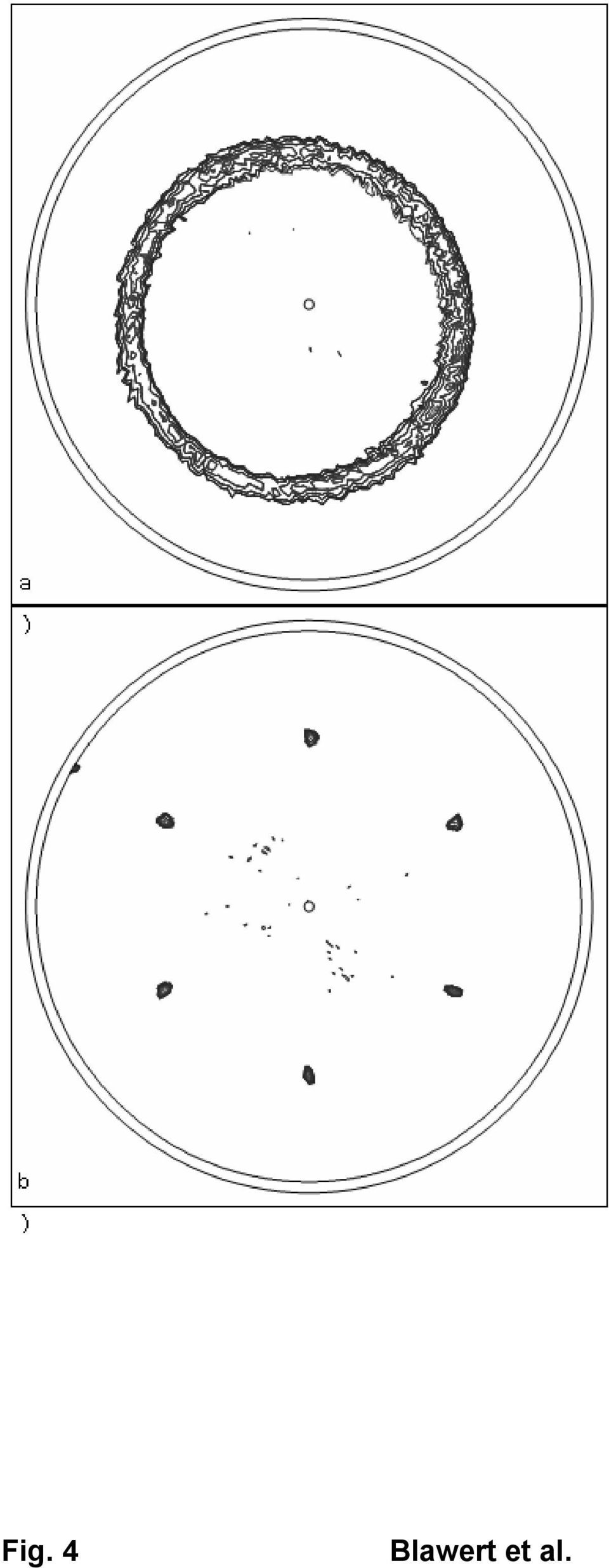
7 the average particle energies are not representative of the whole energy distribution encountered during the deposition processes. For VAD, no high energy particles are involved, while in MS at the present conditions, collisions will reduce the flux and the maximum energy of Ar + ions reflected from the cathode [18]. However, in IBS at considerably lower pressures, necessary to transport the ion beam from the source to the sputter target, the reflected primary ions will reach the substrate without further reductions in energy. As a consequence, these ions can penetrate the growing film beyond the first few monolayers. Independent of the detailed model explaining the preferential growth with either the channelling direction [19], preferential sputtering [20] or deformation energy minimization [21] determining the final texture, these energetic ions are a necessary condition for highly textured film growth. However, a certain influence of the surface free energy of the growing Mg must be additionally present as a preferred growth of the basal planes parallel to the surface is even present at very low energy deposition. In addition, an influence of the alloying composition is also present, with Mg-Al-Zr film deposited by IBS showing a FWHM in the Mg(002) rocking curve of less than 1 [22], compared to 3 for cp-mg in the present case. A third component determining the texture, beside the high energy particle flux and the surface energy as a function of orientation, is the structure of the substrate. For deposition on Si, covered with a native amorphous oxide layer of a few nanometer thickness, a fibre texture was found, as indicated by the (101) pole figure for cp-mg deposited on Si by IBS in Fig. 4a. The same pole figure for a film deposited by VAD onto c-plane sapphire substrates depicted in Fig. 4b with a lattice mismatch of 10 15%, in contrast, shows a high-quality epitaxial growth. Surprisingly, the corrosion properties show no significant influence of the process or ion energy thus of the observed texture changes. Although the corrosion rate for cp-mg films varies between 144 and 293 µm/year for VAD and IBS films, the potential (indicating the driving force for dissolution) is only changing from 1712 to 1739 mv being within the 7

8 typical error of ± 20 mv between different measurements on the same type of coating (see Fig. 5). However compared to as-cast Mg the corrosion potential itself is shifted by about 200 mv towards more negative values. It can be speculated whether this shift in the corrosion potential is caused by the preferred orientation of the films with the c-axis nearly normal to the surface or the increasing amount of grain boundaries. Nevertheless the variations in orientation distribution function encountered for the three methods, as presented above, do not constitute a large influence on the free corrosion potential. The effect on the corrosion rate is visible, but the calculation of the corrosion rates assume a perfect surface and the same surface area for the three processes, not accounting for the changing surface roughness as visible in Fig. 1. MS and IBS with similar surface roughness have similar corrosion rate of 260 and 293 µm/year while the smoother VAD specimen has only 144 µm/year, suggesting that this is most likely a roughness and no texture effect. 4. Summary & Conclusions Commercially pure Mg coatings can be deposited using different PVD techniques with the corresponding morphology closely related with the average energy per deposited particle according to the standard models for energetic film deposition. However, the texture evolution, especially the pronounced c-axis texture as measured by the FWHM of the Mg(002) reflection is highly susceptive to the high energy component delivered by reflected Ar + ions in ion beam sputtering. Additional influences of the substrate material and the alloying system are present. No larger differences in the corrosion properties of the deposited films as a function of the preparation method were found, when the roughness effect on the corrosion rate is considered. Nevertheless, the significant shift of the corrosion potential of pure Mg by 200 mv towards more negative values, which allows the possibility of cathodic protection layers, has still to be accounted for. The texture change between the three deposition processes is too small to be visible in the corrosion behaviour. 8

9 Acknowledgements The authors acknowledge the German Research Foundation (DFG) for funding the research work within the priority programme 1168: Erweiterung der Einsatzgrenzen von Magnesiumlegierungen. 9

10 References [1] K.U. Kainer, Magnesium: Eigenschaften, Anwendungen, Potentiale, (VCH, Weinheim, 2000). [2] M.O. Pekguleryuz and A.A. Kaya, Adv. Eng. Mat. 5 (2003) 866. [3] C. Potzies and K.U. Kainer, Adv. Eng. Mat. 6 (2004) 281. [4] Z. Bin Sajuri, T. Umehara, Y. Miyashita, and Y. Mutoh, Adv. Eng. Mat. 5 (2003) 910. [5] G. Song and A. Atrens, Adv. Eng. Mat. 5 (2003) 837. [6] A. Yamamoto A. Watanabe, K. Sugahara, H. Tsubakino, S. Fukumoto, Scripta Mater. 44 (2001) [7] H. Hoche, H. Scheerer, S. Flege, E.Broszeit, C. Berger, and H. M. Ortner, Mat.-wiss. u. Werkstofftech. 32 (2001) 259. [8] J.A. Thornton, J. Vac. Sci. Technol. A 4 (1974) 666. [9] Y. Bohne, D.M. Seeger, C. Blawert, W. Dietzel, S. Mändl, and B. Rauschenbach, Surf. Coat. Technol. 200 (2006) [10] C. Blawert, V. Heitmann, W. Dietzel, M. Störmer, Y. Bohne, S. Mändl, and B. Rauschenbach, Mat. Sci. Forum (2007) [11] C. Blawert, Y. Bohne, W. Dietzel, and S. Mändl, Formation and Corrosion Properties of Mg-Ti Alloys Prepared By Physical Vapour Deposition, Plasma Proc. Polymers (in press). [12] D.M. Seeger, C. Blawert, W. Dietzel, Y. Bohne, S. Mändl, B. Rauschenbach, Comparison of as-cast and Plasma-Deposited Commercial Magnesium Alloys, in Magnesium Technology 2005, eds. N.R. Neelameggham, H.I. Kaplan, B.R. Powell (The Minerals, Metals & Materials Society, 2005), pp [13] A. Grigucevičienè, K. Leinartas, R. Juškènas, and E. Juzeliūnas, J. Electroanal. Chem. 565 (2004) 203. [14] M.H. Lee, I.Y. Bae, K.J. Kim, K.M. Moon, and T. Oki, Surf Coat. Technol (2003) 670. [15] M. Störmer, C. Blawert, H. Hagen, V. Heitmann, and W. Dietzel, Plasma Process. Polym. 4 (2007) S557. [16] M. Zeuner, F. Scholze, H. Neumann, T. Chassé, G. Otto, D. Roth, A. Hellmich, and B. Ocker, Surf. Coat. Techn. 142/144 (2001)
![Sugahara, H. Tsubakino, S. Fukumoto, Scripta Mater. 44 (2001) 1039. [7] H. Hoche, H. Scheerer, S. Flege, E.Broszeit, C. Berger, and H. M. Ortner, Mat.-wiss. u. Werkstofftech. 32 (2001) 259. [8] J.A.](/docs-images/53/11072288/images/page_10.jpg "Thornton, J. Vac. Sci. Technol. A 4 (1974) 666. [9] Y. Bohne, D.M. Seeger, C. Blawert, W. Dietzel, S. Mändl, and B. Rauschenbach, Surf. Coat. Technol. 200 (2006) 6527. [10] C. Blawert, V. Heitmann, W.")
11 [17] S. Mändl, Y. Bohne, J.W. Gerlach, W. Assmann, and B. Rauschenbach, Nucl. Instrum. Meth. B 249 (2006) 297. [18] K. Ellmer, J. Phys. D: Appl. Phys. 33 (2000) R17. [19] G.N. Van Wyk and H.J. Smith, Nucl. Instr. Meth. A 170 (1980) 443. [20] R.M. Bradley, J.M.E Harper, and D.A. Smith, J. Appl. Phys. 60 (1986) [21] J. Pelleg, L.Z. Zervin, S. Lingo, and N. Croitoru, Thin Solid Fims 197 (1991) 117. [22] Y. Bohne, D. Manova, C. Blawert, M. Störmer, W. Dietzel, and S. Mändl, Nucl. Instrum. Meth B 257 (2007)
![A. Smith, J. Appl. Phys. 60 (1986) 4160. [21] J. Pelleg, L.Z. Zervin, S. Lingo, and N. Croitoru, Thin Solid Fims 197 (1991) 117.](/docs-images/53/11072288/images/page_11.jpg "[22] Y. Bohne, D. Manova, C. Blawert, M. Störmer, W. Dietzel, and S. Mändl, Nucl. Instrum. Meth B 257 (2007) 392. 11")
12 Figure Captions Fig. 1: Surface morphology of cp-mg films deposited by (a) MS, (b) IBS, and (c) VAD. Fig. 2: XRD spectra measured in Bragg-Brentano geometry of cp-mg films produced by IBS and vacuum arc deposition. The diamond symbols indicate the expected positions for Mg (PDF ). Fig. 3: Corresponding Mg(002) rocking curves. Fig. 4: Mg(101) pole figures for cpibs-mg films deposited (a) by IBS onto Si and (b) VAD onto c-axis oriented sapphire. Fig. 5: Polarization curves for cp-mg produced by IBS, MS and VAD (0.5% NaCl, ph11). 12
 pole figures for cpibs-mg films deposited (a) by IBS onto Si and (b) VAD onto c-axis oriented sapphire. Fig.")
13 a) 1 µm b) 1 µm c) 2 µm Fig. 1 Blawert et al.

14 Intensity (a. u.) (002) VAD θ/2θ Geometry Si substrate (004) IBS Angle 2θ (degree) Fig. 2 Blawert et al.

15 Intensity (a. u.) Rocking Curves MS IBS VAD Angle θ (degree) Fig. 3 Blawert et al.
 Fig.")
16 Fig. 4 Blawert et al.
17 Fig. 5 Blawert et al.

Final Draft of the original manuscript:
 Final Draft of the original manuscript: Bohne, Y.; Manova, D.; Blawert, C.; Stoermer, M.; Dietzel, W.; Maendl, S.: Influence of ion energy on morphology and corrosion properties of Mg alloys formed by
2. Deposition process
 Properties of optical thin films produced by reactive low voltage ion plating (RLVIP) Antje Hallbauer Thin Film Technology Institute of Ion Physics & Applied Physics University of Innsbruck Investigations
Vacuum Evaporation Recap
 Sputtering Vacuum Evaporation Recap Use high temperatures at high vacuum to evaporate (eject) atoms or molecules off a material surface. Use ballistic flow to transport them to a substrate and deposit.
EXPERIMENTAL STUDY OF STRUCTURAL ZONE MODEL FOR COMPOSITE THIN FILMS IN MAGNETIC RECORDING MEDIA APPLICATION
 EXPERIMENTAL STUDY OF STRUCTURAL ZONE MODEL FOR COMPOSITE THIN FILMS IN MAGNETIC RECORDING MEDIA APPLICATION Hua Yuan and David E. Laughlin Department of Materials Science and Engineering, Carnegie Mellon
Coating Technology: Evaporation Vs Sputtering
 Satisloh Italy S.r.l. Coating Technology: Evaporation Vs Sputtering Gianni Monaco, PhD R&D project manager, Satisloh Italy 04.04.2016 V1 The aim of this document is to provide basic technical information
Lecture 12. Physical Vapor Deposition: Evaporation and Sputtering Reading: Chapter 12. ECE 6450 - Dr. Alan Doolittle
 Lecture 12 Physical Vapor Deposition: Evaporation and Sputtering Reading: Chapter 12 Evaporation and Sputtering (Metalization) Evaporation For all devices, there is a need to go from semiconductor to metal.
Sputtered AlN Thin Films on Si and Electrodes for MEMS Resonators: Relationship Between Surface Quality Microstructure and Film Properties
 Sputtered AlN Thin Films on and Electrodes for MEMS Resonators: Relationship Between Surface Quality Microstructure and Film Properties S. Mishin, D. R. Marx and B. Sylvia, Advanced Modular Sputtering,
Ion Beam Sputtering: Practical Applications to Electron Microscopy
 Ion Beam Sputtering: Practical Applications to Electron Microscopy Applications Laboratory Report Introduction Electron microscope specimens, both scanning (SEM) and transmission (TEM), often require a
h e l p s y o u C O N T R O L
 contamination analysis for compound semiconductors ANALYTICAL SERVICES B u r i e d d e f e c t s, E v a n s A n a l y t i c a l g r o u p h e l p s y o u C O N T R O L C O N T A M I N A T I O N Contamination
Microscopy and Nanoindentation. Combining Orientation Imaging. to investigate localized. deformation behaviour. Felix Reinauer
 Combining Orientation Imaging Microscopy and Nanoindentation to investigate localized deformation behaviour Felix Reinauer René de Kloe Matt Nowell Introduction Anisotropy in crystalline materials Presentation
DIEGO TONINI MORPHOLOGY OF NIOBIUM FILMS SPUTTERED AT DIFFERENT TARGET SUBSTRATE ANGLE
 UNIVERSITÀ DEGLI STUDI DI PADOVA SCIENCE FACULTY MATERIAL SCIENCE DEGREE INFN LABORATORI NAZIONALI DI LEGNARO DIEGO TONINI MORPHOLOGY OF NIOBIUM FILMS SPUTTERED AT DIFFERENT TARGET SUBSTRATE ANGLE 2 QUESTIONS
The study of structural and optical properties of TiO 2 :Tb thin films
 Optica Applicata, Vol. XXXVII, No. 4, 2007 The study of structural and optical properties of TiO 2 :Tb thin films AGNIESZKA BORKOWSKA, JAROSLAW DOMARADZKI, DANUTA KACZMAREK, DAMIAN WOJCIESZAK Faculty of
State of the art in reactive magnetron sputtering
 State of the art in reactive magnetron sputtering T. Nyberg, O. Kappertz, T. Kubart and S. Berg Solid State Electronics, The Ångström Laboratory, Uppsala University, Box 534, S-751 21 Uppsala, Sweden D.
THIN FILM MATERIALS TECHNOLOGY
 THIN FILM MATERIALS TECHNOLOGY Sputtering of Compound Materials by Kiyotaka Wasa Yokohama City University Yokohama, Japan Makoto Kitabatake Matsushita Electric Industrial Co., Ltd. Kyoto, Japan Hideaki
NANOSTRUCTURED ZnO AND ZAO TRANSPARENT THIN FILMS BY SPUTTERING SURFACE CHARACTERIZATION
 Rev.Adv.Mater.Sci. Nanostructured ZnO 10 and (2005) ZAO 335-340 transparent thin films by sputtering surface characterization 335 NANOSTRUCTURED ZnO AND ZAO TRANSPARENT THIN FILMS BY SPUTTERING SURFACE
Chemical Sputtering. von Kohlenstoff durch Wasserstoff. W. Jacob
 Chemical Sputtering von Kohlenstoff durch Wasserstoff W. Jacob Centre for Interdisciplinary Plasma Science Max-Planck-Institut für Plasmaphysik, 85748 Garching Content: Definitions: Chemical erosion, physical
Glancing XRD and XRF for the Study of Texture Development in SmCo Based Films Sputtered Onto Silicon Substrates
 161 162 Glancing XRD and XRF for the Study of Texture Development in SmCo Based Films Sputtered Onto Silicon Substrates F. J. Cadieu*, I. Vander, Y. Rong, and R. W. Zuneska Physics Department Queens College
Optical Properties of Sputtered Tantalum Nitride Films Determined by Spectroscopic Ellipsometry
 Optical Properties of Sputtered Tantalum Nitride Films Determined by Spectroscopic Ellipsometry Thomas Waechtler a, Bernd Gruska b, Sven Zimmermann a, Stefan E. Schulz a, Thomas Gessner a a Chemnitz University
Decorative vacuum coating technologies 30.05.2014 Certottica Longarone. Thin Film Plasma Coating Technologies
 Dr. Stefan Schlichtherle Dr. Georg Strauss PhysTech Coating Technology GmbH Decorative vacuum coating technologies 30.05.2014 Certottica Longarone Thin Film Plasma Coating Technologies Content The fascination
Chapter 8. Low energy ion scattering study of Fe 4 N on Cu(100)
") Low energy ion scattering study of 4 on Cu(1) Chapter 8. Low energy ion scattering study of 4 on Cu(1) 8.1. Introduction For a better understanding of the reconstructed 4 surfaces one would like to know
Low energy ion scattering study of 4 on Cu(1) Chapter 8. Low energy ion scattering study of 4 on Cu(1) 8.1. Introduction For a better understanding of the reconstructed 4 surfaces one would like to know
OPTIMIZING OF THERMAL EVAPORATION PROCESS COMPARED TO MAGNETRON SPUTTERING FOR FABRICATION OF TITANIA QUANTUM DOTS
 OPTIMIZING OF THERMAL EVAPORATION PROCESS COMPARED TO MAGNETRON SPUTTERING FOR FABRICATION OF TITANIA QUANTUM DOTS Vojtěch SVATOŠ 1, Jana DRBOHLAVOVÁ 1, Marian MÁRIK 1, Jan PEKÁREK 1, Jana CHOMOCKÁ 1,
Paper No. 4071 APPLICATION OF EQCM TO THE STUDY OF CO2 CORROSION
 Paper No. 471 APPLICATION OF EQCM TO THE STUDY OF CO2 CORROSION Yang Yang, Bruce Brown and Srdjan Nešić Institute for Corrosion and Multiphase Technology, Department of Chemical and Biomolecular Engineering
High quality superconducting niobium films produced by Ultra High Vacuum
 High quality superconducting niobium films produced by Ultra High Vacuum Cathodic Arc R. Russo a Dipartimento di Fisica, Università degli studi di Roma Tor Vergata, 00133 Roma, Italy and Istituto di Cibernetica
X-ray Diffraction and EBSD
 X-ray Diffraction and EBSD Jonathan Cowen Swagelok Center for the Surface Analysis of Materials Case School of Engineering Case Western Reserve University October 27, 2014 Outline X-ray Diffraction (XRD)
Laser beam sintering of coatings and structures
 Laser beam sintering of coatings and structures Anne- Maria Reinecke, Peter Regenfuß, Maren Nieher, Sascha Klötzer, Robby Ebert, Horst Exner Laserinstitut Mittelsachsen e.v. an der Hochschule Mittweida,
Applications of New, High Intensity X-Ray Optics - Normal and thin film diffraction using a parabolic, multilayer mirror
 Applications of New, High Intensity X-Ray Optics - Normal and thin film diffraction using a parabolic, multilayer mirror Stephen B. Robie scintag, Inc. 10040 Bubb Road Cupertino, CA 95014 Abstract Corundum
Stress and Microstructure of Sputter Deposited Thin Copper and Niobium Films
 Max-Planck-Institut für Metallforschung Stuttgart Stress and Microstructure of Sputter Deposited Thin Copper and Niobium Films Brando Chidi Okolo Dissertation an der Universität Stuttgart Bericht Nr. 132
Final Draft of the original manuscript:
 Final Draft of the original manuscript: Srinivasan, P.B.; Scharnagl, N.; Blawert, C.; Dietzel, W.: Enhanced corrosion protection of AZ31 magnesium alloy by duplex plasma electrolytic oxidation and polymer
A Multilayer Clad Aluminum Material with Improved Brazing Properties
 A Multilayer Clad Aluminum Material with Improved Brazing Properties An interlayer between cladding and core is shown to be an effective barrier against silicon penetration during brazing BY H. ENGSTROM
Modification of Pd-H 2 and Pd-D 2 thin films processed by He-Ne laser
 Modification of Pd-H 2 and Pd-D 2 thin films processed by He-Ne laser V.Nassisi #, G.Caretto #, A. Lorusso #, D.Manno %, L.Famà %, G.Buccolieri %, A.Buccolieri %, U.Mastromatteo* # Laboratory of Applied
Microhardness study of Ti(C, N) films deposited on S-316 by the Hallow Cathode Discharge Gun
 films deposited on S-316 by the Hallow Cathode Discharge Gun") of Achievements in Materials and Manufacturing Engineering VOLUME 14 ISSUE 1-2 January-February 2006 Microhardness study of Ti(C, N) films deposited on S-316 by the Hallow Cathode Discharge Gun A.J. Novinrooz*,
of Achievements in Materials and Manufacturing Engineering VOLUME 14 ISSUE 1-2 January-February 2006 Microhardness study of Ti(C, N) films deposited on S-316 by the Hallow Cathode Discharge Gun A.J. Novinrooz*,
Coating Thickness and Composition Analysis by Micro-EDXRF
 Application Note: XRF Coating Thickness and Composition Analysis by Micro-EDXRF www.edax.com Coating Thickness and Composition Analysis by Micro-EDXRF Introduction: The use of coatings in the modern manufacturing
Study on the early stage of thin filmgrowth in pulsed beamdeposition by kinetic Monte Carlo simulation
 Surface and Coatings Technology 158 159 (2002) 247 252 Study on the early stage of thin filmgrowth in pulsed beamdeposition by kinetic Monte Carlo simulation a, b Q.Y. Zhang *, P.K. Chu a State Key Laboratory
Materials Sciences. Dr.-Ing. Norbert Hort norbert.hort@gkss.de. International Masters Programme in Biomedical Engineering
 Materials Sciences International Masters Programme in Biomedical Engineering Magnesium Innovations Center (MagIC) GKSS Forschungszentrum Geesthacht GmbH Dr.-Ing. Norbert Hort norbert.hort@gkss.de Contents
Plasma monitoring of plasma-assisted nitriding of aluminium alloys
 Surface and Coatings Technology 120 121 (1999) 244 249 www.elsevier.nl/locate/surfcoat Plasma monitoring of plasma-assisted nitriding of aluminium alloys Michael Quast *, Peter Mayr, Heinz-Rolf Stock Stiftung
Exploring the deposition of oxides on silicon for photovoltaic cells by pulsed laser deposition
 Applied Surface Science 186 2002) 453±457 Exploring the deposition of oxides on silicon for photovoltaic cells by pulsed laser deposition Lianne M. Doeswijk a,*, Hugo H.C. de Moor b, Horst Rogalla a, Dave
HYDROGEN STORAGE AND MICROSTRUCTURE INVESTIGATIONS OF La 0.7- Av. Prof. Lineu Prestes, 2242, ZIP 05508-000, São Paulo, Brazil.
 HYDROGEN STORAGE AND MICROSTRUCTURE INVESTIGATIONS OF La 0.7- x Pr x ALLOYS G. S. Galdino 1,a, J. C. S. Casini 1, E. A. Ferreira 1, R. N. Faria 1, H. Takiishi 1 a gsgaldino@ipen.br 1 Department of Metallurgy,
X-ray thin-film measurement techniques
 Technical articles X-ray thin-film measurement techniques II. Out-of-plane diffraction measurements Toru Mitsunaga* 1. Introduction A thin-film sample is two-dimensionally formed on the surface of a substrate,
Introduction to Thin Film Technology LOT. Chair of Surface and Materials Technology
 Introduction to Thin Film Introduction to Thin Film Verfahrenstechnik der Oberflächenmodifikationen Prof. Dr. Xin Jiang Lecture Institut für Werkstofftechnik der Uni-Siegen Sommersemester 2007 Introduction
Phase Characterization of TiO 2 Powder by XRD and TEM
 Kasetsart J. (Nat. Sci.) 42 : 357-361 (28) Phase Characterization of TiO 2 Powder by XRD and TEM Kheamrutai Thamaphat 1 *, Pichet Limsuwan 1 and Boonlaer Ngotawornchai 2 ABSTRACT In this study, the commercial
Cathodic Arc Deposition of superconducting thin films of MgB 2 for RF cavities*
 Alameda Applied Sciences Corporation Cathodic Arc Deposition of superconducting thin films of MgB 2 for RF cavities* Mahadevan Krishnan, Andrew Gerhan, Kristi Wilson and Brian Bures Alameda Applied Sciences
Adsorption at Surfaces
 Adsorption at Surfaces Adsorption is the accumulation of particles (adsorbate) at a surface (adsorbent or substrate). The reverse process is called desorption. fractional surface coverage: θ = Number of
Tecnologie convenzionali nell approccio top-down; I: metodi e problematiche per la deposizione di film sottili
 LS Scienza dei Materiali - a.a. 2005/06 Fisica delle Nanotecnologie part 8 Version 4, Dec 2005 Francesco Fuso, tel 0502214305, 0502214293 - fuso@df.unipi.it http://www.df.unipi.it/~fuso/dida Tecnologie
Sn-Cu Intermetallic Grain Morphology Related to Sn Layer Thickness
 Journal of ELECTRONIC MATERIALS, Vol. 36, No. 11, 2007 DOI: 10.1007/s11664-007-0270-x Ó 2007 TMS Special Issue Paper -Cu Intermetallic Grain Morphology Related to Layer Thickness MIN-HSIEN LU 1 and KER-CHANG
Chapter 4 Indium Tin Oxide Films Deposited by d.c. Sputtering
 Chapter 4 Indium Tin Oxide Films Deposited by d.c. Sputtering 4.1. Introduction Indium-tin-oxide (ITO) thin films are widely used in optoelectronics devices, flat panel display and electrochromic (EC)
Surface characterization of oxygen deficient SrTiO 3
 U. Scotti di Uccio Surface characterization of oxygen deficient SrTiO 3 films and single crystals Coherentia-CNR-INFM Napoli, Italy Prof. R. Vaglio R. Di Capua, G. De Luca, M. Radovic, N. Lampis, P. Perna,
Lecture: 33. Solidification of Weld Metal
 Lecture: 33 Solidification of Weld Metal This chapter presents common solidification mechanisms observed in weld metal and different modes of solidification. Influence of welding speed and heat input on
Types of Epitaxy. Homoepitaxy. Heteroepitaxy
 Epitaxy Epitaxial Growth Epitaxy means the growth of a single crystal film on top of a crystalline substrate. For most thin film applications (hard and soft coatings, optical coatings, protective coatings)
Cross-Interaction Between Au and Cu in Au/Sn/Cu Ternary Diffusion Couples
 Cross-Interaction Between Au and Cu in Au/Sn/Cu Ternary Diffusion Couples C. W. Chang 1, Q. P. Lee 1, C. E. Ho 1 1, 2, *, and C. R. Kao 1 Department of Chemical & Materials Engineering 2 Institute of Materials
Direct Energy Influx Measurements. in Low Pressure Plasma Processes
 Direct Energy Influx Measurements in Low Pressure Plasma Processes A.L. Thomann, GREMI Orléans R. Dussart, N. Semmar, J. Mathias, T. Lecas L. Bedra, P.A. Cormier, V. Dolique Outline I. Introduction: Why
SELECTIVE DISSOLUTION AND CORROSION FATIGUE BEHAVIORS OF 2205 DUPLEX STAINLESS STEEL
 W.-T. Tsai, I.-H. Lo Department of Materials Science and Engineering National Cheng Kung University Tainan, Taiwan SELECTIVE DISSOLUTION AND CORROSION FATIGUE BEHAVIORS OF 2205 DUPLEX STAINLESS STEEL ABSTRACT
MICROSTRUCTURAL AND MECHANICAL CHARACTERIZATION OF GRAY CAST IRON AND AlSi ALLOY AFTER LASER BEAM HARDENING
 Materials Science Forum Vols. 638-642 (2010) pp 769-774 Online available since 2010/Jan/12 at www.scientific.net (2010) Trans Tech Publications, Switzerland doi:10.4028/www.scientific.net/msf.638-642.769
Chemical vapor deposition of novel carbon materials
 Thin Solid Films 368 (2000) 193±197 www.elsevier.com/locate/tsf Chemical vapor deposition of novel carbon materials L. Chow a, b, *, D. Zhou b, c, A. Hussain b, c, S. Kleckley a, K. Zollinger a, A. Schulte
Deposition of Thin Metal Films " (on Polymer Substrates)!
!") Deposition of Thin Metal Films " (on Polymer Substrates)! Shefford P. Baker! Cornell University! Department of Materials Science and Engineering! Ithaca, New York, 14853! MS&E 5420 Flexible Electronics,
Deposition of Thin Metal Films " (on Polymer Substrates)! Shefford P. Baker! Cornell University! Department of Materials Science and Engineering! Ithaca, New York, 14853! MS&E 5420 Flexible Electronics,
ESRF Upgrade Phase II: le nuove opportunitá per le linee da magnete curvante
 LUCI DI SINCROTRONE CNR, ROMA 22 APRILE 2014 ESRF Upgrade Phase II: le nuove opportunitá per le linee da magnete curvante Sakura Pascarelli sakura@esrf.fr Page 2 INCREASE IN BRILLIANCE H emittance V emittance
HPPMS/DC-MSIP (Cr,Al,V)N and (Cr,Al,W)N Thin Films for High Temperature Application
N and (Cr,Al,W)N Thin Films for High Temperature Application") HPPMS/DC-MSIP (Cr,Al,V)N and (Cr,Al,W)N Thin Films for High Temperature Application Sebastian Theiß K. Bobzin, N. Bagcivan, M. Ewering, R. H. Brugnara April 23, 21 HPPMS/HiPIMS/MPP Workshop, Golden Outline
HPPMS/DC-MSIP (Cr,Al,V)N and (Cr,Al,W)N Thin Films for High Temperature Application Sebastian Theiß K. Bobzin, N. Bagcivan, M. Ewering, R. H. Brugnara April 23, 21 HPPMS/HiPIMS/MPP Workshop, Golden Outline
The interaction of Cu(100)-Fe surfaces with oxygen studied with photoelectron spectroscopy. I
-Fe surfaces with oxygen studied with photoelectron spectroscopy. I") 5 The interaction of Cu(100)-Fe surfaces with oxygen studied with photoelectron spectroscopy. I Mg Kα excited photoemission. Abstract The oxidation of Cu(100)-Fe surfaces was studied using XPS. Surfaces
5 The interaction of Cu(100)-Fe surfaces with oxygen studied with photoelectron spectroscopy. I Mg Kα excited photoemission. Abstract The oxidation of Cu(100)-Fe surfaces was studied using XPS. Surfaces
MSE 528 - PRECIPITATION HARDENING IN 7075 ALUMINUM ALLOY
 MSE 528 - PRECIPITATION HARDENING IN 7075 ALUMINUM ALLOY Objective To study the time and temperature variations in the hardness and electrical conductivity of Al-Zn-Mg-Cu high strength alloy on isothermal
Neuere Entwicklungen zur Herstellung optischer Schichten durch reaktive. Wolfgang Hentsch, Dr. Reinhard Fendler. FHR Anlagenbau GmbH
 Neuere Entwicklungen zur Herstellung optischer Schichten durch reaktive Sputtertechnologien Wolfgang Hentsch, Dr. Reinhard Fendler FHR Anlagenbau GmbH Germany Contents: 1. FHR Anlagenbau GmbH in Brief
Defects Introduction. Bonding + Structure + Defects. Properties
 Defects Introduction Bonding + Structure + Defects Properties The processing determines the defects Composition Bonding type Structure of Crystalline Processing factors Defects Microstructure Types of
MORPHOLOGY OF NIOBIUM FILMS SPUTTERED AT DIFFERENT TARGET SUBSTRATE ANGLE
 MORPHOLOGY OF NIOBIUM FILMS SPUTTERED AT DIFFERENT TARGET SUBSTRATE ANGLE D. Tonini *, C. Greggio, G. Keppel, F. Laviano $, M. Musiani, G. Torzo and V. Palmieri * Università degli Studi di Padova; INFN-LNL
X-ray diffraction techniques for thin films
 X-ray diffraction techniques for thin films Rigaku Corporation Application Laboratory Takayuki Konya 1 Today s contents (PM) Introduction X-ray diffraction method Out-of-Plane In-Plane Pole figure Reciprocal
DURABILITY OF MORTAR LININGS IN DUCTILE IRON PIPES Durability of mortar linings
 DURABILITY OF MORTAR LININGS IN DUCTILE IRON PIPES Durability of mortar linings I. S. MELAND SINTEF Civil and Environmental Engineering, Cement and Concrete, Trondheim, Norway Durability of Building Materials
Conductivity of silicon can be changed several orders of magnitude by introducing impurity atoms in silicon crystal lattice.
 CMOS Processing Technology Silicon: a semiconductor with resistance between that of conductor and an insulator. Conductivity of silicon can be changed several orders of magnitude by introducing impurity
The effect of film thickness on physical properties of fluorine-doped indium oxide thin films
 Materials Science-Poland, Vol. 22, No. 2, 2004 The effect of film thickness on physical properties of fluorine-doped indium oxide thin films S. M. ROZATI *, T. GANJ Physics Department, University of Guilan,
Polymer growth rate in a wire chamber with oxygen, water, or alcohol gas additives
 SLAC-PUB-13 June 6, 8 Polymer growth rate in a wire chamber with oxygen, water, or alcohol gas additives Adam M. Boyarski Stanford Linear Accelerator Center, M.S. 95, 575 Sand Hill Rd, Menlo Park, CA 95,
Improvement of surface porosity and properties of alumina films by incorporation of Fe micrograins in micro-arc oxidation
 Applied Surface Science 253 (2006) 863 868 www.elsevier.com/locate/apsusc Improvement of surface porosity and properties of alumina films by incorporation of Fe micrograins in micro-arc oxidation Fanya
BIOACTIVE COATINGS ON 316L STAINLESS STEEL IMPLANTS
 Trends Biomater. Artif. Organs. Vol. 17(2) pp 43-47 (2004) http//www.sbaoi.org BIOACTIVE COATINGS ON 316L STAINLESS STEEL IMPLANTS N. Ramesh Babu*,+, Sushant Manwatkar*, K. Prasada Rao* and T. S. Sampath
The study of deep-level emission center in ZnO films grown on c-al 2 O 3 substrates
 The study of deep-level emission center in ZnO films grown on c-al 2 O 3 substrates Guotong Du Yuantao Zhang, Jinzhong Wang, Yongguo Cui (College of Electronic Science and Engineering, State Key Laboratory
Reactive Sputtering Using a Dual-Anode Magnetron System
 Reactive Sputtering Using a Dual-Anode Magnetron System A. Belkind and Z. Zhao, Stevens Institute of Technology, Hoboken, NJ; and D. Carter, G. McDonough, G. Roche, and R. Scholl, Advanced Energy Industries,
RAPIDLY SOLIDIFIED COPPER ALLOYS RIBBONS
 Association of Metallurgical Engineers of Serbia AMES Scientific paper UDC:669.35-153.881-412.2=20 RAPIDLY SOLIDIFIED COPPER ALLOYS RIBBONS M. ŠULER 1, L. KOSEC 1, A. C. KNEISSL 2, M. BIZJAK 1, K. RAIĆ
BNG 331 Cell-Tissue Material Interactions. Biomaterial Surfaces
 BNG 331 Cell-Tissue Material Interactions Biomaterial Surfaces Course update Updated syllabus Homework 4 due today LBL 5 Friday Schedule for today: Chapter 8 Biomaterial surface characterization Surface
ORIENTATION CHARACTERISTICS OF THE MICROSTRUCTURE OF MATERIALS
 ORIENTATION CHARACTERISTICS OF THE MICROSTRUCTURE OF MATERIALS K. Sztwiertnia Polish Academy of Sciences, Institute of Metallurgy and Materials Science, 25 Reymonta St., 30-059 Krakow, Poland MMN 2009
Size effects. Lecture 6 OUTLINE
 Size effects 1 MTX9100 Nanomaterials Lecture 6 OUTLINE -Why does size influence the material s properties? -How does size influence the material s performance? -Why are properties of nanoscale objects
CONSOLIDATION AND HIGH STRAIN RATE MECHANICAL BEHAVIOR OF NANOCRYSTALLINE TANTALUM POWDER
 CONSOLIDATION AND HIGH STRAIN RATE MECHANICAL BEHAVIOR OF NANOCRYSTALLINE TANTALUM POWDER Sang H. Yoo, T.S. Sudarshan, Krupa Sethuram Materials Modification Inc, 2929-P1 Eskridge Rd, Fairfax, VA, 22031
* This work is an official contribution of the National Institute of Standards and Technology and
 Variability in the Geometric Accuracy of Additively Manufactured Test Parts A.L. Cooke and J.A. Soons National Institute of Standards and Technology * Gaithersburg, MD, USA Abstract This paper describes
COMPARISON OF TEXTURE IN COPPER AND ALUMINUM THIN FILMS DETERMINED BY XRD AND EBSD *
 201 COMPARISON OF TEXTURE IN COPPER AND ALUMINUM THIN FILMS DETERMINED BY XRD AND EBSD * J. Müller 1, D. Balzar 1,2, R.H. Geiss 1, D.T. Read 1, and R.R. Keller 1 1 Materials Reliability Division, National
Nanoparticle Deposition on Packaging Materials by the Liquid Flame Spray
 Nanoparticle Deposition on Packaging Materials by the Liquid Flame Spray Hannu Teisala a, Mikko Tuominen a, Mikko Aromaa b, Jyrki M. Mäkelä b, Milena Stepien c, Jarkko J. Saarinen c, Martti Toivakka c
Plasma Electronic is Partner of. Tailor-Made Surfaces by Plasma Technology
 Precision Fair 2013 Stand 171 Plasma Electronic is Partner of Tailor-Made Surfaces by Plasma Technology Dr. J. Geng, Plasma Electronic GmbH Modern Surface Technology in 1900 Overview A short introduction
Introduction to VLSI Fabrication Technologies. Emanuele Baravelli
 Introduction to VLSI Fabrication Technologies Emanuele Baravelli 27/09/2005 Organization Materials Used in VLSI Fabrication VLSI Fabrication Technologies Overview of Fabrication Methods Device simulation
This is an author-deposited version published in: http://sam.ensam.eu Handle ID:.http://hdl.handle.net/10985/10324
 Science Arts & Métiers (SAM) is an open access repository that collects the work of Arts et Métiers ParisTech researchers and makes it freely available over the web where possible. This is an author-deposited
Ch. 4: Imperfections in Solids Part 1. Dr. Feras Fraige
 Ch. 4: Imperfections in Solids Part 1 Dr. Feras Fraige Outline Defects in Solids 0D, Point defects vacancies Interstitials impurities, weight and atomic composition 1D, Dislocations edge screw 2D, Grain
The New PVD HI3-Technology: Latest Developments and Potential for Coining Dies.
 The New PVD HI3-Technology: Latest Developments and Potential for Coining Dies. Technical Forum - World Money Fair 2015, Berlin 29 th January 2015, Oerlikon The New Segment Surface Solutions Segment Manmade
Supporting information
 Supporting information Ultrafast room-temperature NH 3 sensing with positively-gated reduced graphene oxide field-effect transistors Ganhua Lu 1, Kehan Yu 1, Leonidas E. Ocola 2, and Junhong Chen 1 * 1
Electron Microscopy 3. SEM. Image formation, detection, resolution, signal to noise ratio, interaction volume, contrasts
 Electron Microscopy 3. SEM Image formation, detection, resolution, signal to noise ratio, interaction volume, contrasts 3-1 SEM is easy! Just focus and shoot "Photo"!!! Please comment this picture... Any
The atomic packing factor is defined as the ratio of sphere volume to the total unit cell volume, or APF = V S V C. = 2(sphere volume) = 2 = V C = 4R
 = 2 = V C = 4R") 3.5 Show that the atomic packing factor for BCC is 0.68. The atomic packing factor is defined as the ratio of sphere volume to the total unit cell volume, or APF = V S V C Since there are two spheres associated
3.5 Show that the atomic packing factor for BCC is 0.68. The atomic packing factor is defined as the ratio of sphere volume to the total unit cell volume, or APF = V S V C Since there are two spheres associated
View of ΣIGMA TM (Ref. 1)
") Overview of the FESEM system 1. Electron optical column 2. Specimen chamber 3. EDS detector [Electron Dispersive Spectroscopy] 4. Monitors 5. BSD (Back scatter detector) 6. Personal Computer 7. ON/STANDBY/OFF
Overview of the FESEM system 1. Electron optical column 2. Specimen chamber 3. EDS detector [Electron Dispersive Spectroscopy] 4. Monitors 5. BSD (Back scatter detector) 6. Personal Computer 7. ON/STANDBY/OFF
The Focused Ion Beam Scanning Electron Microscope: A tool for sample preparation, two and three dimensional imaging. Jacob R.
 The Focused Ion Beam Scanning Electron Microscope: A tool for sample preparation, two and three dimensional imaging Jacob R. Bowen Contents Components of a FIB-SEM Ion interactions Deposition & patterns
Oxidation behaviour of Ti 3 SiC 2 -based ceramic at 900±1300 C in air
 Corrosion Science 43 2001) 1095±1109 www.elsevier.com/locate/corsci Oxidation behaviour of Ti 3 SiC 2 -based ceramic at 900±1300 C in air Zhimei Sun a, Yanchun Zhou a, *, Meishuan Li b a Department of
Wafer Manufacturing. Reading Assignments: Plummer, Chap 3.1~3.4
 Wafer Manufacturing Reading Assignments: Plummer, Chap 3.1~3.4 1 Periodic Table Roman letters give valence of the Elements 2 Why Silicon? First transistor, Shockley, Bardeen, Brattain1947 Made by Germanium
III. Wet and Dry Etching
 III. Wet and Dry Etching Method Environment and Equipment Advantage Disadvantage Directionality Wet Chemical Solutions Atmosphere, Bath 1) Low cost, easy to implement 2) High etching rate 3) Good selectivity
Characterization of sputtered NiO thin films
 Surface & Coatings Technology 198 (2005) 138 142 www.elsevier.com/locate/surfcoat Characterization of sputtered NiO thin films Hao-Long Chen a, *, Yang-Ming Lu b, Weng-Sing Hwang a a Department of Materials
Scanning Electron Microscopy Services for Pharmaceutical Manufacturers
 Scanning Electron Microscopy Services for Pharmaceutical Manufacturers Author: Gary Brake, Marketing Manager Date: August 1, 2013 Analytical Testing Laboratory www.atl.semtechsolutions.com Scanning Electron
Structure and properties of transparent conductive ZnO films grown by pulsed laser
 Structure and properties of transparent conductive ZnO films grown by pulsed laser deposition (PLD) by Yu Hsiu, Lin A dissertation submitted to the University of Birmingham for the degree of Master of
MOLECULAR DYNAMICS INVESTIGATION OF DEFORMATION RESPONSE OF THIN-FILM METALLIC NANOSTRUCTURES UNDER HEATING
 NANOSYSTEMS: PHYSICS, CHEMISTRY, MATHEMATICS, 2011, 2 (2), P. 76 83 UDC 538.97 MOLECULAR DYNAMICS INVESTIGATION OF DEFORMATION RESPONSE OF THIN-FILM METALLIC NANOSTRUCTURES UNDER HEATING I. S. Konovalenko
Keywords: Planar waveguides, sol-gel technology, transmission electron microscopy
 Structural and optical characterisation of planar waveguides obtained via Sol-Gel F. Rey-García, C. Gómez-Reino, M.T. Flores-Arias, G.F. De La Fuente, W. Assenmacher, W. Mader ABSTRACT Planar waveguides
Effect of the oxide film formed on the electrical properties of Cu-Zn alloy electric contact material
 Effect of the oxide film formed on the electrical properties of Cu-Zn alloy electric contact material Hao-Long Chen *, Ke-Cheng Tseng and Yao-Sheng Yang Department of Electronic Engineering, Kao Yuan University,
Thin film structures of diamond-like carbon prepared by pulsed plasma techniques 325. Publications
 PUBLICATIONS 324 Publications Thin film structures of diamond-like carbon prepared by pulsed plasma techniques 325 Publications The following list includes the published papers, attended conferences and
Secondary Ion Mass Spectrometry
 Secondary Ion Mass Spectrometry A PRACTICAL HANDBOOK FOR DEPTH PROFILING AND BULK IMPURITY ANALYSIS R. G. Wilson Hughes Research Laboratories Malibu, California F. A. Stevie AT&T Bell Laboratories Allentown,
Solidification, Crystallization & Glass Transition
 Solidification, Crystallization & Glass Transition Cooling the Melt solidification Crystallization versus Formation of Glass Parameters related to the formaton of glass Effect of cooling rate Glass transition