Introduction to Thin Film Technology LOT. Chair of Surface and Materials Technology
|
|
|
- Prosper Jefferson
- 10 years ago
- Views:
Transcription
1 Introduction to Thin Film Introduction to Thin Film Verfahrenstechnik der Oberflächenmodifikationen Prof. Dr. Xin Jiang Lecture Institut für Werkstofftechnik der Uni-Siegen Sommersemester 2007

2 Introduction to Thin Film FACHBEREICH MASCHINENBAU Institut für Energietechnik Institut für Mechanik und Regelungstechnik - Mechatronik Institut für Fertigungstechnik Institut für Systemtechnik Institut für Fluidund Thermodynamik Institut für Werkstofftechnik Institut für Konstruktion

3 Introduction to Thin Film Institut für Werkstofftechnik Lehrstuhl für Materialkunde und Werkstoffprüfung Prof. Dr.-Ing. H.-J. Christ Lehrstuhl für Oberflächen- und Werkstofftechnologie Prof. Dr. rer. nat. X. Jiang

4 Introduction to Thin Film Forschungsschwerpunkte des Schichtsysteme ht t Superharte Schichten Funktionsschichten ht Kompositschichten Nanomaterialien Kohlenstoffbasierte Nanostrukturen Nanokomposite o Galvanische Nanostrukturen Werkstoffanalytik Strukturuntersuchungen Bestimmung von Material/Systemeigenschaften

5 Introduction to Thin Film Stil der Vorlesung - Skript: Kopie der Folien (Internet) - Vorlesung mit PP-Präsentation, Präsentation überwiegend auf Englisch -Prüfung (mündlich) Zeit und Raum werden vereinbart
 Zeit und Raum werden")
6 Introduction to Thin Film Contents 1. Introduction and Application Examples (2h) 2. Vacuum Technique (1h) 2.1 Kinetics of Gases 2.22 Transport and Pumping of Gases 2.3 Pumping Systems Preparation of Thin Films by PVD (Physical Vapor Deposition) (10h) 2.2 Evaporation (3h) Thermal Evaporation Evaporation of alloy and compound films Reactive Evaporation Activated Reactive Evaporation Other modern Evaporation Techniques 2.3 Sputtering (4h) Physical Principals of the Processes Further Processes in Film Growth by Sputtering Sputtering of Alloys Reactive Sputtering Technical Setups of Sputtering 2.4 Production of Thin Films by Ions and ionized Clusters (0,5h) Characteristic Data of the Particles and their Influences on the Growth of the thin films (1,5h) 3 Preparation of Thin Films by CVD (Chemical Vapor Deposition) (4h) 3.1 Conventional CVD Processes 3.2 Plasma-Assisted CVD Plasma Decomposition (a-c:h C:H, a-si:h) Microwave-Plasma-Assisted Diamond Deposition 4 Important Film Systems (2h)
 25 2.")
7 Introduction to Thin Film Literatures 1. M. Ohring, "The materials science of thin films" (Academic Press 1992). 2. R. Kern et al., Basic Mechanisms in the early stages of epitaxy in Current Topics in Materials Science, vol 3, series Editor E. Kaldis, p IFF-Ferienkurs Dünne Schichten, März H. K. Pulker, Coatings on Glass, Thin Films Science and, 6, Elsevier K. Reichelt and X. Jiang, Thin Solid Films 191, (1990).

8 Introduction to Thin Film Definition How is the Thin Film defined? Which h topics are included d in the Surface?

9 Introduction to Thin Film The cleavage of a crystal: creation of new surfaces Break of the bonds Reconstruction of the surface atom Section perpendicular to the line of cleavage

10 Introduction to Thin Film Surface reconstruction The real crystal has broken (unoccupied) bonds on its surface which may lead to the surface reconstruction. (100) Si surface before reconstruction (rotated 4x4x2 and 6x6x2 lattices). White and blue balls show two FCC sublattices of Si. 2x1 reconstruction of (100) Si surface (RGBW colored and 6x6x2 lattices).

11 Introduction to Thin Film Real surface topography of metals (V) Contamination layer (IV) Adsorption layer (III) Reaction layer (II) Deformations layer (I) () Volume
 Deformations layer")
12 Introduction to Thin Film Scientific areas Å to nm surface physics/chemistry/technique nm to µm physics/chemistry/technique of thin films Bulk properties dominited Bulk material solid state physics/chemistry/technique

13 Introduction to Thin Film Development of electronics Vakuumelekt ronik Fest körperelekt ronik 10-4 Mikroelekt ronik 10-6 Int egriert e Mikroelekt ronik 10-8 Molekulare Elekt ronik Jahr

14 Introduction to Thin Film Introduction to Thin Film The course provides foundations in thin film deposition; emphases the most used techniques. Modern thin film technology has evolved into a sophisticated set of techniques used to increase performance and aesthetic value of many products and make new functional systems and devices. There are following categories of thin film deposition Physical vapor deposition (PVD) Chemical vapor deposition (CVD) Chemical methods Electrochemical methods Combinations of these methods gives a large number of deposition techniques with unique impact on the thin film formation.
 Chemical vapor deposition (CVD) Chemical methods Electrochemical")
15 Introduction to Thin Film Thin Films and Deposition Thin films Monolayer - several micrometers Thin film properties may be different from those of bulk Quantum confinement effect: quantum and size surface/area ratio effects quantum dots Thin Film Deposition Thin films can be deposited under non-equilibrium conditions Solid - Melting -Vaporization- Condensation-Solidification Vapor - Reaction -Condensation-Solidification Gas/vapor- Plasma- Reaction-Condensation-Solidification

16 Introduction to Thin Film Application areas of thin films and surface engineering Electronics Flexible Polymer Light Emitting Displays Optical coatings Anti-reflex films for liens systems und umbrella glass Supra-conductive films SQUIDs Magnetic films Storage & reading Environment & energy technique low E window glass coating Heat prevention & corrosion resistance Turbine blade coating Super hard coatings Wear resistance of machine parts and tools

17 Introduction to Thin Film Thin Film Applications Variety of tool coatings: DLC / TiC / TiN, graphitic i-c, TiAlN, etc DryCoat Inc

18 Introduction to Thin Film Thin Film Applications
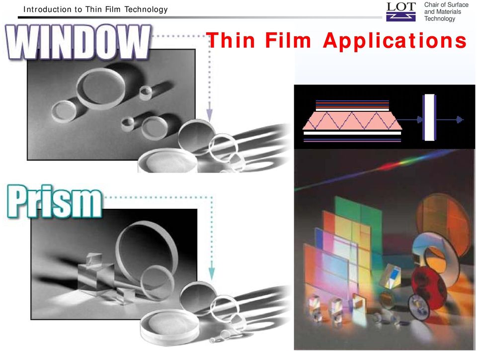
19 Introduction to Thin Film Optical functional films Anti-reflex films 2 R = n 0 n 2 n 0 + n 2 R = I refl. / I inc. n 2 =1,52 refraction index for glass n 2 = 1,0 refraction index for vacuum > 8% light lost by reflection. The reflection will be reduced by coating a selected film (MgF 2 ) of certain fraction index (n 1 = 1,38) and thickness: n = = λ 1 n 0 n 2 t 4

20 Introduction to Thin Film Thin Film Applications

21 Introduction to Thin Film Thin Film Applications Patinor
22 Introduction to Thin Film Thin Film Applications
23 Introduction to Thin Film Thin Film Applications
24 Introduction to Thin Film Tools coated with a-c:h filma
25 Introduction to Thin Film Films for the energy technique Glass Oxide block layer Ag layer
26 Introduction to Thin Film Research Fundamental Development of new materials Material behavior Applied Development of new products devices and systems Enhancement of the product performance Increase of product value including aesthetic value
27 Introduction to Thin Film Films and surface technology in the research Quanten Hall-Effekt
28 Introduction to Thin Film Band discontinuity of the semiconductor
Coating Technology: Evaporation Vs Sputtering
 Satisloh Italy S.r.l. Coating Technology: Evaporation Vs Sputtering Gianni Monaco, PhD R&D project manager, Satisloh Italy 04.04.2016 V1 The aim of this document is to provide basic technical information
2. Deposition process
 Properties of optical thin films produced by reactive low voltage ion plating (RLVIP) Antje Hallbauer Thin Film Technology Institute of Ion Physics & Applied Physics University of Innsbruck Investigations
Plasma Electronic is Partner of. Tailor-Made Surfaces by Plasma Technology
 Precision Fair 2013 Stand 171 Plasma Electronic is Partner of Tailor-Made Surfaces by Plasma Technology Dr. J. Geng, Plasma Electronic GmbH Modern Surface Technology in 1900 Overview A short introduction
Introduction to VLSI Fabrication Technologies. Emanuele Baravelli
 Introduction to VLSI Fabrication Technologies Emanuele Baravelli 27/09/2005 Organization Materials Used in VLSI Fabrication VLSI Fabrication Technologies Overview of Fabrication Methods Device simulation
OPTIMIZING OF THERMAL EVAPORATION PROCESS COMPARED TO MAGNETRON SPUTTERING FOR FABRICATION OF TITANIA QUANTUM DOTS
 OPTIMIZING OF THERMAL EVAPORATION PROCESS COMPARED TO MAGNETRON SPUTTERING FOR FABRICATION OF TITANIA QUANTUM DOTS Vojtěch SVATOŠ 1, Jana DRBOHLAVOVÁ 1, Marian MÁRIK 1, Jan PEKÁREK 1, Jana CHOMOCKÁ 1,
Decorative vacuum coating technologies 30.05.2014 Certottica Longarone. Thin Film Plasma Coating Technologies
 Dr. Stefan Schlichtherle Dr. Georg Strauss PhysTech Coating Technology GmbH Decorative vacuum coating technologies 30.05.2014 Certottica Longarone Thin Film Plasma Coating Technologies Content The fascination
Types of Epitaxy. Homoepitaxy. Heteroepitaxy
 Epitaxy Epitaxial Growth Epitaxy means the growth of a single crystal film on top of a crystalline substrate. For most thin film applications (hard and soft coatings, optical coatings, protective coatings)
Chemical Synthesis. Overview. Chemical Synthesis of Nanocrystals. Self-Assembly of Nanocrystals. Example: Cu 146 Se 73 (PPh 3 ) 30
 30") Chemical Synthesis Spontaneous organization of molecules into stable, structurally well-defined aggregates at the nanometer length scale. Overview The 1-100 nm nanoscale length is in between traditional
Chemical Synthesis Spontaneous organization of molecules into stable, structurally well-defined aggregates at the nanometer length scale. Overview The 1-100 nm nanoscale length is in between traditional
Conductivity of silicon can be changed several orders of magnitude by introducing impurity atoms in silicon crystal lattice.
 CMOS Processing Technology Silicon: a semiconductor with resistance between that of conductor and an insulator. Conductivity of silicon can be changed several orders of magnitude by introducing impurity
ALD Atomic Layer Deposition
 Research - Services ALD Atomic Layer Deposition Atomic Layer Deposition is a deposition process for assembling of thin films on the nanometer scale. The self-limiting deposition of atomic monolayers occurs
Vacuum Evaporation Recap
 Sputtering Vacuum Evaporation Recap Use high temperatures at high vacuum to evaporate (eject) atoms or molecules off a material surface. Use ballistic flow to transport them to a substrate and deposit.
1. Photon Beam Damage and Charging at Solid Surfaces John H. Thomas III
 1. Photon Beam Damage and Charging at Solid Surfaces John H. Thomas III 1. Introduction............................. 2. Electrostatic Charging of Samples in Photoemission Experiments............................
Adsorption at Surfaces
 Adsorption at Surfaces Adsorption is the accumulation of particles (adsorbate) at a surface (adsorbent or substrate). The reverse process is called desorption. fractional surface coverage: θ = Number of
Chemical Sputtering. von Kohlenstoff durch Wasserstoff. W. Jacob
 Chemical Sputtering von Kohlenstoff durch Wasserstoff W. Jacob Centre for Interdisciplinary Plasma Science Max-Planck-Institut für Plasmaphysik, 85748 Garching Content: Definitions: Chemical erosion, physical
Lecture 9. Surface Treatment, Coating, Cleaning
 1 Lecture 9. Surface Treatment, Coating, Cleaning These processes are sometimes referred to as post-processing. They play a very important role in the appearance, function and life of the product. Broadly,
Picosun World Forum, Espoo 9.6.2009. 35 years of ALD. Tuomo Suntola, Picosun Oy. Tuomo Suntola, Picosun Oy
 35 years of ALD Conventional methods for compound film deposition Heat treatment Final crystallization Nucleation Vacuum evaporation Sputtering CVD Buildup of thin film in source controlled deposition
Combustion chemical vapor deposition
 V I P Combustion chemical vapor deposition A technology to improve adhesion on surfaces to be coated Volkmar J. Eigenbrod, Christina Hensch, Alexander Kemper Introduction Combustion chemical vapor deposition
Unit 12 Practice Test
 Name: Class: Date: ID: A Unit 12 Practice Test Multiple Choice Identify the choice that best completes the statement or answers the question. 1) A solid has a very high melting point, great hardness, and
Neuere Entwicklungen zur Herstellung optischer Schichten durch reaktive. Wolfgang Hentsch, Dr. Reinhard Fendler. FHR Anlagenbau GmbH
 Neuere Entwicklungen zur Herstellung optischer Schichten durch reaktive Sputtertechnologien Wolfgang Hentsch, Dr. Reinhard Fendler FHR Anlagenbau GmbH Germany Contents: 1. FHR Anlagenbau GmbH in Brief
2. Nanoparticles. Introduction to Nanoscience, 2005 1
 2. Nanoparticles Nanoparticles are the simplest form of structures with sizes in the nm range. In principle any collection of atoms bonded together with a structural radius of < 100 nm can be considered
For Touch Panel and LCD Sputtering/PECVD/ Wet Processing
 production Systems For Touch Panel and LCD Sputtering/PECVD/ Wet Processing Pilot and Production Systems Process Solutions with over 20 Years of Know-how Process Technology at a Glance for Touch Panel,
The New PVD HI3-Technology: Latest Developments and Potential for Coining Dies.
 The New PVD HI3-Technology: Latest Developments and Potential for Coining Dies. Technical Forum - World Money Fair 2015, Berlin 29 th January 2015, Oerlikon The New Segment Surface Solutions Segment Manmade
III. Wet and Dry Etching
 III. Wet and Dry Etching Method Environment and Equipment Advantage Disadvantage Directionality Wet Chemical Solutions Atmosphere, Bath 1) Low cost, easy to implement 2) High etching rate 3) Good selectivity
Chapter 7-1. Definition of ALD
 Chapter 7-1 Atomic Layer Deposition (ALD) Definition of ALD Brief history of ALD ALD process and equipments ALD applications 1 Definition of ALD ALD is a method of applying thin films to various substrates
Technology White Papers nr. 13 Paul Holister Cristina Román Vas Tim Harper
 QUANTUM DOTS Technology White Papers nr. 13 Paul Holister Cristina Román Vas Tim Harper QUANTUM DOTS Technology White Papers nr. 13 Release Date: Published by Científica Científica, Ltd. www.cientifica.com
Materials Sciences. Dr.-Ing. Norbert Hort [email protected]. International Masters Programme in Biomedical Engineering
 Materials Sciences International Masters Programme in Biomedical Engineering Magnesium Innovations Center (MagIC) GKSS Forschungszentrum Geesthacht GmbH Dr.-Ing. Norbert Hort [email protected] Contents
Graphene a material for the future
 Graphene a material for the future by Olav Thorsen What is graphene? What is graphene? Simply put, it is a thin layer of pure carbon What is graphene? Simply put, it is a thin layer of pure carbon It has
Dry Etching and Reactive Ion Etching (RIE)
") Dry Etching and Reactive Ion Etching (RIE) MEMS 5611 Feb 19 th 2013 Shengkui Gao Contents refer slides from UC Berkeley, Georgia Tech., KU, etc. (see reference) 1 Contents Etching and its terminologies
Dry Etching and Reactive Ion Etching (RIE) MEMS 5611 Feb 19 th 2013 Shengkui Gao Contents refer slides from UC Berkeley, Georgia Tech., KU, etc. (see reference) 1 Contents Etching and its terminologies
Deposition of Thin Metal Films " (on Polymer Substrates)!
!") Deposition of Thin Metal Films " (on Polymer Substrates)! Shefford P. Baker! Cornell University! Department of Materials Science and Engineering! Ithaca, New York, 14853! MS&E 5420 Flexible Electronics,
Deposition of Thin Metal Films " (on Polymer Substrates)! Shefford P. Baker! Cornell University! Department of Materials Science and Engineering! Ithaca, New York, 14853! MS&E 5420 Flexible Electronics,
Science Standard Articulated by Grade Level Strand 5: Physical Science
 Concept 1: Properties of Objects and Materials Classify objects and materials by their observable properties. Kindergarten Grade 1 Grade 2 Grade 3 Grade 4 PO 1. Identify the following observable properties
Lecture 12. Physical Vapor Deposition: Evaporation and Sputtering Reading: Chapter 12. ECE 6450 - Dr. Alan Doolittle
 Lecture 12 Physical Vapor Deposition: Evaporation and Sputtering Reading: Chapter 12 Evaporation and Sputtering (Metalization) Evaporation For all devices, there is a need to go from semiconductor to metal.
Dr Marcin Adamiak marcin.adamiak. www.imiib.polsl.pl/
 FP7 NMP/INCO Brokerage Event Warsaw, 17-18 September 2009 Dr Marcin Adamiak marcin.adamiak [email protected] http://www.imiib.polsl.pl www.imiib.polsl.pl/ Institute of Engineering Materials and Biomaterials
Matter, Materials, Crystal Structure and Bonding. Chris J. Pickard
 Matter, Materials, Crystal Structure and Bonding Chris J. Pickard Why should a theorist care? Where the atoms are determines what they do Where the atoms can be determines what we can do Overview of Structure
h e l p s y o u C O N T R O L
 contamination analysis for compound semiconductors ANALYTICAL SERVICES B u r i e d d e f e c t s, E v a n s A n a l y t i c a l g r o u p h e l p s y o u C O N T R O L C O N T A M I N A T I O N Contamination
Part B 2. Allow a total of 15 credits for this part. The student must answer all questions in this part.
 Part B 2 Allow a total of 15 credits for this part. The student must answer all questions in this part. 51 [1] Allow 1 credit for 3 Mg(s) N 2 (g) Mg 3 N 2 (s). Allow credit even if the coefficient 1 is
High Rate Oxide Deposition onto Web by Reactive Sputtering from Rotatable Magnetrons
 High Rate Oxide Deposition onto Web by Reactive Sputtering from Rotatable Magnetrons D.Monaghan, V. Bellido-Gonzalez, M. Audronis. B. Daniel Gencoa, Physics Rd, Liverpool, L24 9HP, UK. www.gencoa.com,
Deposition of Silicon Oxide, Silicon Nitride and Silicon Carbide Thin Films by New Plasma Enhanced Chemical Vapor Deposition Source Technology
 General Plasma, Inc. 546 East 25th Street Tucson, Arizona 85713 tel. 520-882-5100 fax. 520-882-5165 and Silicon Carbide Thin Films by New Plasma Enhanced Chemical Vapor Deposition Source Technology M.
Physical Properties and Functionalization of Low-Dimensional Materials
 Physical Properties and Functionalization of Low-Dimensional Materials Physics Department, University of Trieste Graduate School of Physics, XXVI cycle Supervisor: Co-supervisor: Prof. Alessandro BARALDI
State of the art in reactive magnetron sputtering
 State of the art in reactive magnetron sputtering T. Nyberg, O. Kappertz, T. Kubart and S. Berg Solid State Electronics, The Ångström Laboratory, Uppsala University, Box 534, S-751 21 Uppsala, Sweden D.
The study of structural and optical properties of TiO 2 :Tb thin films
 Optica Applicata, Vol. XXXVII, No. 4, 2007 The study of structural and optical properties of TiO 2 :Tb thin films AGNIESZKA BORKOWSKA, JAROSLAW DOMARADZKI, DANUTA KACZMAREK, DAMIAN WOJCIESZAK Faculty of
ANSWER KEY. Energy Levels, Electrons and IONIC Bonding It s all about the Give and Take!
 ANSWER KEY Energy Levels, Electrons and IONIC Bonding It s all about the Give and Take! From American Chemical Society Middle School Chemistry Unit: Chapter 4 Content Statements: Distinguish the difference
Module 7 Wet and Dry Etching. Class Notes
 Module 7 Wet and Dry Etching Class Notes 1. Introduction Etching techniques are commonly used in the fabrication processes of semiconductor devices to remove selected layers for the purposes of pattern
Tecnologie convenzionali nell approccio top-down; I: metodi e problematiche per la deposizione di film sottili
 LS Scienza dei Materiali - a.a. 2005/06 Fisica delle Nanotecnologie part 8 Version 4, Dec 2005 Francesco Fuso, tel 0502214305, 0502214293 - [email protected] http://www.df.unipi.it/~fuso/dida Tecnologie
The CVD diamond booklet
 available at: www.diamond-materials.com/download Content 1. General properties of diamond... 2 2. Optical Properties... 4 Optical transparency...4 Absorption coefficient at 10.6 µm...5 Refractive index:
High performance. Architectural glazings utilise thin. low-emissivity coating. Coating technology
 Coating technology High performance low-emissivity coating Growing concern with energy efficiency has sparked the development of double low-emissivity coatings in architectural glass. BOC Coating has designed
Untitled Document. 1. Which of the following best describes an atom? 4. Which statement best describes the density of an atom s nucleus?
 Name: Date: 1. Which of the following best describes an atom? A. protons and electrons grouped together in a random pattern B. protons and electrons grouped together in an alternating pattern C. a core
Tableting Punch Performance Can Be Improved With Precision Coatings
 Tableting Punch Performance Can Be Improved With Precision Coatings by Arnold H. Deutchman, Ph. D. Director of Research and Development (614) 873-4529 X 114 [email protected] Mr. Dale C. Natoli
Plasma Cleaner: Physics of Plasma
 Plasma Cleaner: Physics of Plasma Nature of Plasma A plasma is a partially ionized gas consisting of electrons, ions and neutral atoms or molecules The plasma electrons are at a much higher temperatures
Sputtering Targets and Sputtered Films: Technology and Markets
 A BCC Research Semiconductor Manufacturing Report and Sputtered Films: SMC037E Use this report to: Understand the most important advances in sputtering technology and target fabrication Identify the current
Light management for photovoltaics. Ando Kuypers, TNO Program manager Solar
 Light management for photovoltaics Ando Kuypers, TNO Program manager Solar Global energy consumption: 500 ExaJoule/Year Solar irradiation on earth sphere: 5.000.000 ExaJoule/year 2 Capturing 0,01% covers
Ion Beam Sputtering: Practical Applications to Electron Microscopy
 Ion Beam Sputtering: Practical Applications to Electron Microscopy Applications Laboratory Report Introduction Electron microscope specimens, both scanning (SEM) and transmission (TEM), often require a
Implementation Of High-k/Metal Gates In High-Volume Manufacturing
 White Paper Implementation Of High-k/Metal Gates In High-Volume Manufacturing INTRODUCTION There have been significant breakthroughs in IC technology in the past decade. The upper interconnect layers of
Modern Construction Materials Prof. Ravindra Gettu Department of Civil Engineering Indian Institute of Technology, Madras
 Modern Construction Materials Prof. Ravindra Gettu Department of Civil Engineering Indian Institute of Technology, Madras Module - 2 Lecture - 2 Part 2 of 2 Review of Atomic Bonding II We will continue
Optical Properties of Sputtered Tantalum Nitride Films Determined by Spectroscopic Ellipsometry
 Optical Properties of Sputtered Tantalum Nitride Films Determined by Spectroscopic Ellipsometry Thomas Waechtler a, Bernd Gruska b, Sven Zimmermann a, Stefan E. Schulz a, Thomas Gessner a a Chemnitz University
Laser beam sintering of coatings and structures
 Laser beam sintering of coatings and structures Anne- Maria Reinecke, Peter Regenfuß, Maren Nieher, Sascha Klötzer, Robby Ebert, Horst Exner Laserinstitut Mittelsachsen e.v. an der Hochschule Mittweida,
Study of tungsten oxidation in O 2 /H 2 /N 2 downstream plasma
 Study of tungsten oxidation in O 2 /H 2 /N 2 downstream plasma Songlin Xu a and Li Diao Mattson Technology, Inc., Fremont, California 94538 Received 17 September 2007; accepted 21 February 2008; published
COATED CARBIDE. TiN. Al 2 O 3
 COATED CARBIDE GENERAL INFORMATION CVD = Chemical Vapour Deposition coated grades GC2015, GC2025, GC2135, GC235, GC3005, GC3015, GC3020, GC3025, GC3115, GC4015, GC4025, GC4035, S05F, and CD1810. PVD =
The content is based on the National Science Teachers Association (NSTA) standards and is aligned with state standards.
 standards and is aligned with state standards.") Literacy Advantage Physical Science Physical Science Literacy Advantage offers a tightly focused curriculum designed to address fundamental concepts such as the nature and structure of matter, the characteristics
Literacy Advantage Physical Science Physical Science Literacy Advantage offers a tightly focused curriculum designed to address fundamental concepts such as the nature and structure of matter, the characteristics
Introduction to OLED technology 1. General characteristics
 www.osram-oled.com Introduction to OLED technology 1. General characteristics 1.1. Structure An organic light-emitting diode (OLED) consists of several semiconducting organic layers sandwiched between
Keywords: Planar waveguides, sol-gel technology, transmission electron microscopy
 Structural and optical characterisation of planar waveguides obtained via Sol-Gel F. Rey-García, C. Gómez-Reino, M.T. Flores-Arias, G.F. De La Fuente, W. Assenmacher, W. Mader ABSTRACT Planar waveguides
Deposition Overview for Microsytems
 Deposition Overview for Microsytems Deposition PK Activity Terminology Participant Guide www.scme-nm.org Deposition Overview for Microsystems Primary Knowledge Participant Guide Description and Estimated
How To Make A Plasma Control System
 XXII. Erfahrungsaustausch Mühlleiten 2015 Plasmaanalyse und Prozessoptimierung mittels spektroskopischem Plasmamonitoring in industriellen Anwendungen Swen Marke,, Lichtenau Thomas Schütte, Plasus GmbH,
Pulsed laser deposition of organic materials
 Pulsed laser deposition of organic materials PhD theses Gabriella Kecskeméti Department of Optics and Quantum Electronics University of Szeged Supervisor: Dr. Béla Hopp senior research fellow Department
How To Make A Pvd Coating
 Hard and Superhard Nanocomposite Coating deposited by PVD technology for industrial application Dott. Romagnoli Denis STS Service and Tools STS s.r.l. via Parini 12 40033 Casalecchio di Reno(Bo) Tel. 051-969882
Design of inductors and modeling of relevant field intensity
 3. Growth of shaped Si single crystals (FZ) Design of inductors and modeling of relevant field intensity Main cut Schematic of inductor for large square FZ crystals z-component of the field intensity for
Lecture 2 - Semiconductor Physics (I) September 13, 2005
 September 13, 2005") 6.012 - Microelectronic Devices and Circuits - Fall 2005 Lecture 2-1 Lecture 2 - Semiconductor Physics (I) September 13, 2005 Contents: 1. Silicon bond model: electrons and holes 2. Generation and recombination
6.012 - Microelectronic Devices and Circuits - Fall 2005 Lecture 2-1 Lecture 2 - Semiconductor Physics (I) September 13, 2005 Contents: 1. Silicon bond model: electrons and holes 2. Generation and recombination
Turbulence, Heat and Mass Transfer (THMT 09) Poiseuille flow of liquid methane in nanoscopic graphite channels by molecular dynamics simulation
 Poiseuille flow of liquid methane in nanoscopic graphite channels by molecular dynamics simulation") Turbulence, Heat and Mass Transfer (THMT 09) Poiseuille flow of liquid methane in nanoscopic graphite channels by molecular dynamics simulation Sapienza Università di Roma, September 14, 2009 M. T. HORSCH,
Turbulence, Heat and Mass Transfer (THMT 09) Poiseuille flow of liquid methane in nanoscopic graphite channels by molecular dynamics simulation Sapienza Università di Roma, September 14, 2009 M. T. HORSCH,
Common Defects in Digital Printing. Paul Geldenhuys & Amir Shapira January, 2009
 Common Defects in Digital Printing Paul Geldenhuys & Amir Shapira January, 2009 Overview Ambient Influences Humidity Temperature Sunlight & UV Abrasion Chemical Resistance Common Defects in Digital Printing
CHEMISTRY STANDARDS BASED RUBRIC ATOMIC STRUCTURE AND BONDING
 CHEMISTRY STANDARDS BASED RUBRIC ATOMIC STRUCTURE AND BONDING Essential Standard: STUDENTS WILL UNDERSTAND THAT THE PROPERTIES OF MATTER AND THEIR INTERACTIONS ARE A CONSEQUENCE OF THE STRUCTURE OF MATTER,
Structure and properties of transparent conductive ZnO films grown by pulsed laser
 Structure and properties of transparent conductive ZnO films grown by pulsed laser deposition (PLD) by Yu Hsiu, Lin A dissertation submitted to the University of Birmingham for the degree of Master of
Grade Selection... Coated Grades / CVD... Coated Grades / PVD... Cermet... PCBN (T-CBN)... PCD (T-DIA)... Ceramics...
... PCD (T-DIA)... Ceramics...") Products Grade Selection... Coated / CVD... Coated / PVD... Cermet... PCBN (T-CBN)... PCD (T-DIA)... Ceramics... Uncoated Cemented Carbides... Ultra fine Grain Cemented Carbides... -2-4 -6-8 -0-2 - -4-5
Products Grade Selection... Coated / CVD... Coated / PVD... Cermet... PCBN (T-CBN)... PCD (T-DIA)... Ceramics... Uncoated Cemented Carbides... Ultra fine Grain Cemented Carbides... -2-4 -6-8 -0-2 - -4-5
Ch. 4: Imperfections in Solids Part 1. Dr. Feras Fraige
 Ch. 4: Imperfections in Solids Part 1 Dr. Feras Fraige Outline Defects in Solids 0D, Point defects vacancies Interstitials impurities, weight and atomic composition 1D, Dislocations edge screw 2D, Grain
How To Understand Light And Color
 PRACTICE EXAM IV P202 SPRING 2004 1. In two separate double slit experiments, an interference pattern is observed on a screen. In the first experiment, violet light (λ = 754 nm) is used and a second-order
PLASMA TECHNOLOGY OVERVIEW
 PLASMA TECHNOLOGY OVERVIEW Plasmas are not a lab curiosity. Plasma processing has been an essential production tool for more than 30 years in the fabrication of microelectronic devices for example. Over
and LUMINOUS CHEMICAL VAPOR DEPOSITION INTERFACE ENGINEERING HirotsuguYasuda University of Missouri-Columbia Columbia, Missouri, U.S.A.
 LUMINOUS CHEMICAL VAPOR DEPOSITION and INTERFACE ENGINEERING HirotsuguYasuda University of Missouri-Columbia Columbia, Missouri, U.S.A. MARCEL MARCEL DEKKER. NEW YORK DEKKER Contents Preface iii Part I.
Reactive Sputtering Using a Dual-Anode Magnetron System
 Reactive Sputtering Using a Dual-Anode Magnetron System A. Belkind and Z. Zhao, Stevens Institute of Technology, Hoboken, NJ; and D. Carter, G. McDonough, G. Roche, and R. Scholl, Advanced Energy Industries,
Feasibility study on polyparylene deposition in a PECVD reactor
 Institute of Experimental and Applied Physics Feasibility study on polyparylene deposition in a PECVD reactor E. v. Wahl 1, C Kirchberg 2, M. Fröhlich 3, H. Kersten 1 1 IEAP, Group Plasma Technology, University
CHAPTER 10: INTERMOLECULAR FORCES: THE UNIQUENESS OF WATER Problems: 10.2, 10.6,10.15-10.33, 10.35-10.40, 10.56-10.60, 10.101-10.
 CHAPTER 10: INTERMOLECULAR FORCES: THE UNIQUENESS OF WATER Problems: 10.2, 10.6,10.15-10.33, 10.35-10.40, 10.56-10.60, 10.101-10.102 10.1 INTERACTIONS BETWEEN IONS Ion-ion Interactions and Lattice Energy
PHYSISORPTION DETERMINATIONS
 G A S S O R P T I O N A N A L Y S I S PHYSISORPTION DETERMINATIONS Most atoms that make up a solid are bound on all sides by other atoms in the bulk of the solid. The atoms on the surface of the solid,
Lezioni di Tecnologie e Materiali per l Elettronica
 Lezioni di Tecnologie e Materiali per l Elettronica Danilo Manstretta [email protected] microlab.unipv.it Outline Passive components Resistors Capacitors Inductors Printed circuits technologies
Electron Beam and Sputter Deposition Choosing Process Parameters
 Electron Beam and Sputter Deposition Choosing Process Parameters General Introduction The choice of process parameters for any process is determined not only by the physics and/or chemistry of the process,
Metals and Non-metals. Comparison of physical properties of metals and non metals
 Metals and Non-metals Comparison of physical properties of metals and non metals PHYSICAL PROPERTY METALS NON-METALS Physical State Metallic lustre (having a shining surface) Mostly solids (Liquid -mercury)
Chapter 12 - Liquids and Solids
 Chapter 12 - Liquids and Solids 12-1 Liquids I. Properties of Liquids and the Kinetic Molecular Theory A. Fluids 1. Substances that can flow and therefore take the shape of their container B. Relative
THIN FILM MATERIALS TECHNOLOGY
 THIN FILM MATERIALS TECHNOLOGY Sputtering of Compound Materials by Kiyotaka Wasa Yokohama City University Yokohama, Japan Makoto Kitabatake Matsushita Electric Industrial Co., Ltd. Kyoto, Japan Hideaki
Chapter 4 COATINGS Full Reflective Coatings:
 Chapter 4 COATINGS Technical developments in coatings for plastic optics have resulted in optical and durability characteristics once believed possible only with glass. These advances in coating technology
2015-2016 Facility Rates & Expense Caps
 NANOFAB FEES / SERVICES Entry Fee $20.00/Day $32.10/Day Nanofab Training Fee $25.00/Hour $40.13/Hour Nanofab Process Development/Labor $50.00/Hour $80.25/Hour Model Shop $25.00/Month $40.13/Month Wafer
Nano Materials Synthesis, Characterisation and Properties
 Nano Materials Synthesis, Characterisation and Properties Prof. Dr. Cordt Zollfrank Wissenschaftszentrum Weihenstephan Wissenschaftszentrum Straubing Prof. Dr. Johann Plank/ Department Chemie Technische
Study of Surface Reaction and Gas Phase Chemistries in High Density C 4 F 8 /O 2 /Ar and C 4 F 8 /O 2 /Ar/CH 2 F 2 Plasma for Contact Hole Etching
 TRANSACTIONS ON ELECTRICAL AND ELECTRONIC MATERIALS Vol. 16, No. 2, pp. 90-94, April 25, 2015 Regular Paper pissn: 1229-7607 eissn: 2092-7592 DOI: http://dx.doi.org/10.4313/teem.2015.16.2.90 OAK Central:
Technology. Chapter 15 Processing Resources
 Technology Chapter 15 Processing Resources Tools: Printer (color optional) 4 sheets of 8.5 x 11 paper Scissors Directions: 1. Print 2. Fold paper in half vertically 3. Cut along dashed lines These instructions
Lecture 3: Optical Properties of Bulk and Nano. 5 nm
 Lecture 3: Optical Properties of Bulk and Nano 5 nm The Previous Lecture Origin frequency dependence of χ in real materials Lorentz model (harmonic oscillator model) 0 e - n( ) n' n '' n ' = 1 + Nucleus
NANO SILICON DOTS EMBEDDED SIO 2 /SIO 2 MULTILAYERS FOR PV HIGH EFFICIENCY APPLICATION
 NANO SILICON DOTS EMBEDDED SIO 2 /SIO 2 MULTILAYERS FOR PV HIGH EFFICIENCY APPLICATION Olivier Palais, Damien Barakel, David Maestre, Fabrice Gourbilleau and Marcel Pasquinelli 1 Outline Photovoltaic today
Molecular simulation of fluid dynamics on the nanoscale
 VI. International Conference on Computational Fluid Dynamics Molecular simulation of fluid dynamics on the nanoscale St. Petersburg, July 16, 2010 M. Horsch, Y.-Tz. Hsiang, Z. Liu, S. K. Miroshnichenko,
GD-Profiler Series RF Glow Discharge Optical Emission Spectrometers
 GD-Profiler Series RF Glow Discharge Optical Emission Spectrometers For many applications, it is essential to know the chemical composition of a material, both at the surface, at the interfaces and in
VLSI Fabrication Process
 VLSI Fabrication Process Om prakash 5 th sem ASCT, Bhopal [email protected] Manisha Kumari 5 th sem ASCT, Bhopal [email protected] Abstract VLSI stands for "Very Large Scale Integration". This
THIN FILM DEPOSITION TECHNIQUES STEPS TOWARDS MORE SUSTAINABLE PACKAGES
 THIN FILM DEPOSITION TECHNIQUES STEPS TOWARDS MORE SUSTAINABLE PACKAGES Mika Vähä Nissi 1, Terhi Hirvikorpi 1, Tuomas Mustonen 1, Maarit Karppinen 2, Ali Harlin 1 1 VTT Technical Research Centre of Finland,
Warm-Up 9/9. 1. Define the term matter. 2. Name something in this room that is not matter.
 Warm-Up 9/9 1. Define the term matter. 2. Name something in this room that is not matter. Warm-Up 9/16 1. List the three most important rules of lab safety. 2. Would you classify jello as a solid or a
Secondary Ion Mass Spectrometry
 Secondary Ion Mass Spectrometry A PRACTICAL HANDBOOK FOR DEPTH PROFILING AND BULK IMPURITY ANALYSIS R. G. Wilson Hughes Research Laboratories Malibu, California F. A. Stevie AT&T Bell Laboratories Allentown,
Name Class Date. What is ionic bonding? What happens to atoms that gain or lose electrons? What kinds of solids are formed from ionic bonds?
 CHAPTER 1 2 Ionic Bonds SECTION Chemical Bonding BEFORE YOU READ After you read this section, you should be able to answer these questions: What is ionic bonding? What happens to atoms that gain or lose