The New PVD HI3-Technology: Latest Developments and Potential for Coining Dies.
|
|
|
- Kelly Mosley
- 8 years ago
- Views:
Transcription
1 The New PVD HI3-Technology: Latest Developments and Potential for Coining Dies. Technical Forum - World Money Fair 2015, Berlin 29 th January 2015,

2 Oerlikon The New Segment Surface Solutions Segment Manmade Fibers Segment Drive Systems Segment Vacuum Segment Surface Solutions Segment Advanced Technologies Oerlikon Balzers + Sulzer Metco Sulzer Metaplas GmbH Two pioneers under one roof Oerlikon Metaplas GmbH Page 2

3 The merger of Balzers and Metco will form a global technology leader in surface solutions Surface Solutions Segment Transaction summary Signing Jan. 30, 2014 NITRIDING Plasma Nitriding THIN FILM COATING PVD PECVD (PACVD) THICK LAYER COATING Thermal Spray Closing June 2, 2014 Enterprise value of CHF 1 bn Forms the Surface Solutions Segment Surface Solutions to become largest Segment of Oerlikon Group Represents the latest step in Oerlikon s transformation process Positions the Group for long term profitable growth Page 3

4 PVD Technology METAPLAS.DOMINO PVD technology platform PVD coatings - have a high surface hardness - increase wear protection - have high chemical resistance, a low tendency to stick and weld - have an excellent layer adhesion. PVD coatings on coining dies are used for many years now around the world. PVD coatings substantially increase the lifetime of dies and quality of coins. Page 4

5 PVD Technologies offered today Innovative APA Arc Technology High target utilisation Low target cost High deposition rate High Ionization rate (up to 100%) Excellent coating adhesion Magnetron Sputter Technology Wide range of materials Low deposition rate Low Ionization rate (30-40%) Medium coating adhesion Smooth coatings HIPIMS Plasma HiPIMS Sputtering Technology Wide range of materials Low deposition rate High Ionization rate (up to 90%) Very good coating adhesion Very smooth coatings Page 5
 Very good coating adhesion Very")
6 A New Innovative PVD Technology HI3 Technology High Ionization 3 (triple) The Combination of three high ionization processes has been developed. Oerlikon Metaplas has developed and combined 3 technologies with high ionization: AEGD: high ionized plasma etching process APA Arc: high ionized arc coating process HIPIMS: high ionized sputter coating process Page 6


7 High Ionization in PVD Processes A high ionization during the coating process is important because: it is necessary for dense and very smooth coatings better phase and composition control is possible less defects within the coating are produced a high coating adhesion can be achieved Plasma of APA evaporator This provides an excellent tool to design coatings with required improved properties Page 7


8 A New Innovative PVD Technology HI3 Technology For the first time, process and material combinations can be applied, that offer completely new opportunities for high performance PVD coatings. Combined strengths of 3 processes in one PVD system Innovative approach to the next generation of PVD coatings for various applications HI3 Technology allows to achieve layer architectures that could not be realized previously by standard technologies. Page 8

9 A New Innovative PVD Technology Arc specific materials: (Me1Me2Me3X) - CrX - TiX - AlTiX - AlCrX - AlTiCrX -. Magnetron materials: Si, VX, B 4 C top layers on APA Arc coating doping/ nanolayers APA Arc module HiPIMS module Anode of AEGD etching module Page 9

10 First HI3 Coatings have been developed: 1. APA Arc AlTiN + HiPIMS AlTiSiXN H = 2504, E(0.3) = 400 GPa HiPIMS: AlTiSiXN HiPIMS: AlTiSiXN + APA ARC: AlTiN APA ARC: AlTiN First cutting tests showed potential in cutting of stainless steel. However, we are looking for more tailored coatings not only for cutting tools. Page 10

11 First HI3 Coatings have been developed: 2. APA Arc AlTiN + HiPIMS VXN H= /-109, E(0.3) = 419 GPa H= /-131, E(0.3) = 408 GPa HiPIMS: VXN HiPIMS: VXN + APA ARC: AlTiN Hardness /-40, E(0.3) = 345 GPa APA ARC: AlTiN First promising results for taps, stamping and small forming tools. However, we are looking for more tailored coatings also for other for tools. Page 11
 = 345 GPa APA ARC: AlTiN First promising results for taps, stamping and small forming tools.")
12 First HI3 Coatings have been developed: 3. APA Arc AlTiN + HiPIMS SiBCN HiPIMS 1 µm Arc + HiPIMS 3 µm SIBONICA SiBNC: amorphous micro hardness: 20 GPa E-Modulus: 250 GPa AlTiN/SiBNC: fine columnar micro hardness: 28 GPa E-Modulus: 350 GPa Arc 2 µm AlTiN: columnar micro hardness: 27 GPa E-Modulus: 300 GPa SiB based coatings have the highest scientific published oxidation resistance. The alloying with SiB results in a grain refinement of the AlTiN. Page 12

13 Summary HI3 Technology combines the strengths of 3 processes in one PVD system: excellent adhesion, high deposition rate, smooth coatings, economic production Innovative approach to the next generation of PVD coatings for various applications. First developed HI3 coatings show promising results for a wide range of application. With HI3 Technology coatings for coining dies can be tailored by a wide range of materials by micro alloying by doping by design of layer architecture..combined with economical production! HI3 Technology has great potential for improvement according to the needs of coining applications: for circulation coining dies and for proof coining dies. Your are welcome to start testing and improving with us to the best suitable coating for your coining application. Page 13

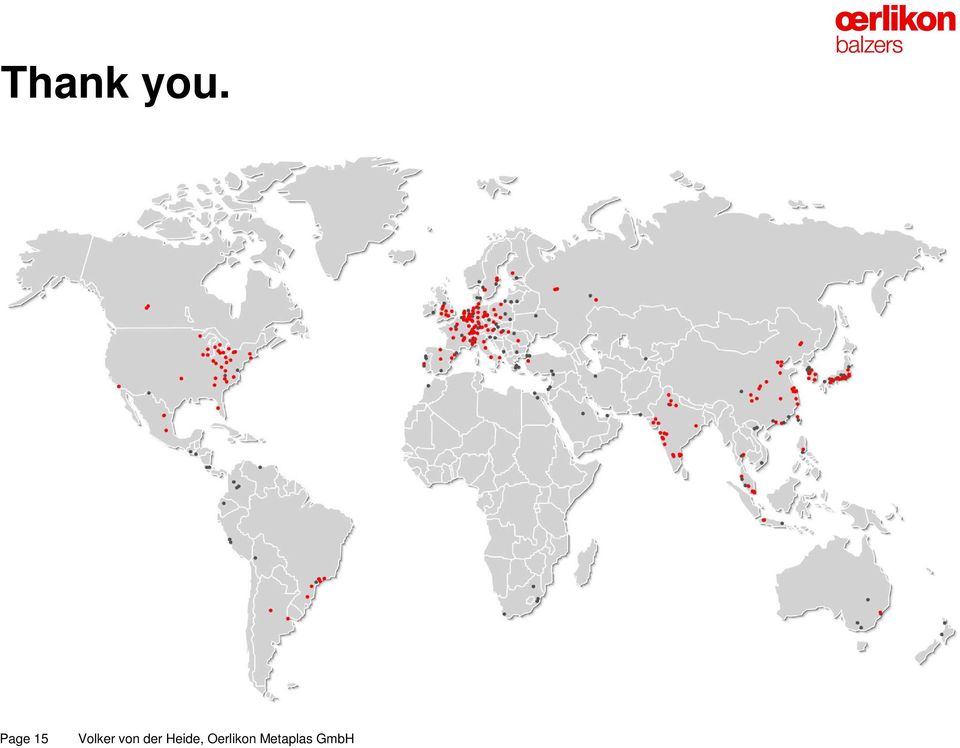
14 References 17 Oerlikon Metaplas PVD coating systems have been installed at mints worldwide: Royal Canadian Mint Casa de Moneda, Mexico Royal Thai Mint, Thailand Ukraine Mint Shenyang Mint, China Mint of Finland, Venezuela Mint Chengdu Mint, China Shanghai Mint, China Nanjing Mint, China Noida Mint, India Page 14

15 Thank you. Page 15
2. Deposition process
 Properties of optical thin films produced by reactive low voltage ion plating (RLVIP) Antje Hallbauer Thin Film Technology Institute of Ion Physics & Applied Physics University of Innsbruck Investigations
For Touch Panel and LCD Sputtering/PECVD/ Wet Processing
 production Systems For Touch Panel and LCD Sputtering/PECVD/ Wet Processing Pilot and Production Systems Process Solutions with over 20 Years of Know-how Process Technology at a Glance for Touch Panel,
Coating Technology: Evaporation Vs Sputtering
 Satisloh Italy S.r.l. Coating Technology: Evaporation Vs Sputtering Gianni Monaco, PhD R&D project manager, Satisloh Italy 04.04.2016 V1 The aim of this document is to provide basic technical information
Coating Solutions for Wind Energy
 Coating Solutions for Wind Energy Wind energy is deemed to be an especially eco-friendly and favorable energy source for power generation. Whether wind power plants work efficiently and economically strongly
How To Make A Pvd Coating
 Hard and Superhard Nanocomposite Coating deposited by PVD technology for industrial application Dott. Romagnoli Denis STS Service and Tools STS s.r.l. via Parini 12 40033 Casalecchio di Reno(Bo) Tel. 051-969882
Plasma Electronic is Partner of. Tailor-Made Surfaces by Plasma Technology
 Precision Fair 2013 Stand 171 Plasma Electronic is Partner of Tailor-Made Surfaces by Plasma Technology Dr. J. Geng, Plasma Electronic GmbH Modern Surface Technology in 1900 Overview A short introduction
THIN FILM MATERIALS TECHNOLOGY
 THIN FILM MATERIALS TECHNOLOGY Sputtering of Compound Materials by Kiyotaka Wasa Yokohama City University Yokohama, Japan Makoto Kitabatake Matsushita Electric Industrial Co., Ltd. Kyoto, Japan Hideaki
Tableting Punch Performance Can Be Improved With Precision Coatings
 Tableting Punch Performance Can Be Improved With Precision Coatings by Arnold H. Deutchman, Ph. D. Director of Research and Development (614) 873-4529 X 114 adeutchman@beamalloy.net Mr. Dale C. Natoli
Warranty. www.tissot.ch 1/5. Warranty
 Warranty Warranty Your TISSOT watch is warranted by TISSOT S.A. for a period of twenty-four (24) months from the date of purchase under the terms and conditions of this warranty. The international TISSOT
Grade Selection... Coated Grades / CVD... Coated Grades / PVD... Cermet... PCBN (T-CBN)... PCD (T-DIA)... Ceramics...
... PCD (T-DIA)... Ceramics...") Products Grade Selection... Coated / CVD... Coated / PVD... Cermet... PCBN (T-CBN)... PCD (T-DIA)... Ceramics... Uncoated Cemented Carbides... Ultra fine Grain Cemented Carbides... -2-4 -6-8 -0-2 - -4-5
Products Grade Selection... Coated / CVD... Coated / PVD... Cermet... PCBN (T-CBN)... PCD (T-DIA)... Ceramics... Uncoated Cemented Carbides... Ultra fine Grain Cemented Carbides... -2-4 -6-8 -0-2 - -4-5
Anodizing Reference Guide
 Anodizing Reference Guide Type Thickness Type II Conventional coatings produced 1.8µ-25.4µ from sulfuric acid bath Type I A Conventional coatings produced 0.5µ-7.6µ (microns) from chromic acid bath Type
Group. The precision company SURFACE TECHNOLOGIES INTERNATIONAL. Aeronautics. Surface solutions by STI Group. English
 Group SURFACE TECHNOLOGIES INTERNATIONAL The precision company Aeronautics English Surface solutions by STI Group AERONAUTIC INDUSTRY Highest Functionality and Safety High-end surface treatment technologies
HARD MILLING OPERATION OF AISI O2 COLD WORK TOOL STEEL BY CARBIDE TOOLS PROTECTED WITH DIFFERENT HARD COATINGS
 JESTECH, 15(1), 21-26, (2012) JESTECH HARD MILLING OPERATION OF AISI O2 COLD WORK TOOL STEEL BY CARBIDE TOOLS PROTECTED WITH DIFFERENT HARD COATINGS Halil Çalışkan *, Cahit Kurbanoğlu **, Davorin Kramar
Sputtering Targets and Sputtered Films: Technology and Markets
 A BCC Research Semiconductor Manufacturing Report and Sputtered Films: SMC037E Use this report to: Understand the most important advances in sputtering technology and target fabrication Identify the current
Neuere Entwicklungen zur Herstellung optischer Schichten durch reaktive. Wolfgang Hentsch, Dr. Reinhard Fendler. FHR Anlagenbau GmbH
 Neuere Entwicklungen zur Herstellung optischer Schichten durch reaktive Sputtertechnologien Wolfgang Hentsch, Dr. Reinhard Fendler FHR Anlagenbau GmbH Germany Contents: 1. FHR Anlagenbau GmbH in Brief
Sputtering Targets and Evaporation Materials for Wear Protection
 Sputtering Targets and Evaporation Materials for Wear Protection Contents About Materials for Wear Protection 3 Overview Sputtering Targets 4 Sputtering Targets 5 Evaporation Materials 7 Nickel Target
histaris Inline Sputtering Systems
 vistaris histaris Inline Sputtering Systems Inline Sputtering Systems with Vertical Substrate Transport Modular System for Different Applications VISTARIS Sputtering Systems The system with the brand name
Lecture 12. Physical Vapor Deposition: Evaporation and Sputtering Reading: Chapter 12. ECE 6450 - Dr. Alan Doolittle
 Lecture 12 Physical Vapor Deposition: Evaporation and Sputtering Reading: Chapter 12 Evaporation and Sputtering (Metalization) Evaporation For all devices, there is a need to go from semiconductor to metal.
Summary of Insert Grades. Insert Lineup Turning Milling Drilling Insert Selection Table Grade Properties PCD CBN. Ceramic. Cell Fiber. Cermet.
 1~15 Summary of Insert Lineup Milling Drilling Insert Selection Table Grade Properties PCD Ceramic Cell Fiber PVD Coated CVD Coated PVD Coated for PVD Coated for Milling and Drilling 2~7 2~3 4 5 5 6 7
IBS - Ion Beam Services
 IBS - Ion Beam Services Profile Technologies Devices & sensor fabricat ion Participation to R&D programs Researched partnership Présentation activité composant 1 Profile : Products and services Product
Sputtered AlN Thin Films on Si and Electrodes for MEMS Resonators: Relationship Between Surface Quality Microstructure and Film Properties
 Sputtered AlN Thin Films on and Electrodes for MEMS Resonators: Relationship Between Surface Quality Microstructure and Film Properties S. Mishin, D. R. Marx and B. Sylvia, Advanced Modular Sputtering,
Ion Beam Sputtering: Practical Applications to Electron Microscopy
 Ion Beam Sputtering: Practical Applications to Electron Microscopy Applications Laboratory Report Introduction Electron microscope specimens, both scanning (SEM) and transmission (TEM), often require a
A Remote Plasma Sputter Process for High Rate Web Coating of Low Temperature Plastic Film with High Quality Thin Film Metals and Insulators
 A Remote Plasma Sputter Process for High Rate Web Coating of Low Temperature Plastic Film with High Quality Thin Film Metals and Insulators Dr Peter Hockley and Professor Mike Thwaites, Plasma Quest Limited
Super Cool Sputter Coater
 Leica EM SCD050 Super Cool Sputter Coater Precious and Non-Precious Metal Sputtering and Carbon Evaporation Sputter Coating The sputter coating of samples inhibits charging, reduces thermal damage and
Decorative vacuum coating technologies 30.05.2014 Certottica Longarone. Thin Film Plasma Coating Technologies
 Dr. Stefan Schlichtherle Dr. Georg Strauss PhysTech Coating Technology GmbH Decorative vacuum coating technologies 30.05.2014 Certottica Longarone Thin Film Plasma Coating Technologies Content The fascination
Introduction to Thin Film Technology LOT. Chair of Surface and Materials Technology
 Introduction to Thin Film Introduction to Thin Film Verfahrenstechnik der Oberflächenmodifikationen Prof. Dr. Xin Jiang Lecture Institut für Werkstofftechnik der Uni-Siegen Sommersemester 2007 Introduction
OPTIMIZING OF THERMAL EVAPORATION PROCESS COMPARED TO MAGNETRON SPUTTERING FOR FABRICATION OF TITANIA QUANTUM DOTS
 OPTIMIZING OF THERMAL EVAPORATION PROCESS COMPARED TO MAGNETRON SPUTTERING FOR FABRICATION OF TITANIA QUANTUM DOTS Vojtěch SVATOŠ 1, Jana DRBOHLAVOVÁ 1, Marian MÁRIK 1, Jan PEKÁREK 1, Jana CHOMOCKÁ 1,
Dr Marcin Adamiak marcin.adamiak. www.imiib.polsl.pl/
 FP7 NMP/INCO Brokerage Event Warsaw, 17-18 September 2009 Dr Marcin Adamiak marcin.adamiak adamiak@polsl.pl http://www.imiib.polsl.pl www.imiib.polsl.pl/ Institute of Engineering Materials and Biomaterials
COATED CARBIDE. TiN. Al 2 O 3
 COATED CARBIDE GENERAL INFORMATION CVD = Chemical Vapour Deposition coated grades GC2015, GC2025, GC2135, GC235, GC3005, GC3015, GC3020, GC3025, GC3115, GC4015, GC4025, GC4035, S05F, and CD1810. PVD =
Technology & Cooperation
 Technology & Cooperation No. 23 April 2014 Hauzer for You 2 No. 23 April 2014 Hauzer for You Content 3 2004-2014 & Beyond 4 Making an Impact with Tribology 6 Microwave Technology, Tribological Progress
Optical Properties of Sputtered Tantalum Nitride Films Determined by Spectroscopic Ellipsometry
 Optical Properties of Sputtered Tantalum Nitride Films Determined by Spectroscopic Ellipsometry Thomas Waechtler a, Bernd Gruska b, Sven Zimmermann a, Stefan E. Schulz a, Thomas Gessner a a Chemnitz University
Solar Photovoltaic (PV) Cells
 Cells") Solar Photovoltaic (PV) Cells A supplement topic to: Mi ti l S Micro-optical Sensors - A MEMS for electric power generation Science of Silicon PV Cells Scientific base for solar PV electric power generation
Solar Photovoltaic (PV) Cells A supplement topic to: Mi ti l S Micro-optical Sensors - A MEMS for electric power generation Science of Silicon PV Cells Scientific base for solar PV electric power generation
Chapter 11 PVD and Metallization
 Chapter 11 PVD and Metallization 2006/5/23 1 Metallization Processes that deposit metal thin film on wafer surface. 2006/5/23 2 1 Metallization Definition Applications PVD vs. CVD Methods Vacuum Metals
Active Nanocomposite Materials
 Active Nanocomposite Materials Contact: Prof. Jorma Jokiniemi (jorma.jokiniemi@uef.fi) The aim of this project was to develop tailored functional nanocomposite materials for industrial applications. The
PVD coatingsin transmissions: case studies I rivestimenti PVD su componenti di trasmissioni: esempi
 PVD coatingsin transmissions: case studies I rivestimenti PVD su componenti di trasmissioni: esempi Paola Recanati Oerlikon Balzers Italy- Precision Components Product Manager Claudio Torrelli Oerlikon
EXPERIMENTAL STUDY OF STRUCTURAL ZONE MODEL FOR COMPOSITE THIN FILMS IN MAGNETIC RECORDING MEDIA APPLICATION
 EXPERIMENTAL STUDY OF STRUCTURAL ZONE MODEL FOR COMPOSITE THIN FILMS IN MAGNETIC RECORDING MEDIA APPLICATION Hua Yuan and David E. Laughlin Department of Materials Science and Engineering, Carnegie Mellon
ALD Atomic Layer Deposition
 Research - Services ALD Atomic Layer Deposition Atomic Layer Deposition is a deposition process for assembling of thin films on the nanometer scale. The self-limiting deposition of atomic monolayers occurs
Vacuum Evaporation Recap
 Sputtering Vacuum Evaporation Recap Use high temperatures at high vacuum to evaporate (eject) atoms or molecules off a material surface. Use ballistic flow to transport them to a substrate and deposit.
Lecture 9. Surface Treatment, Coating, Cleaning
 1 Lecture 9. Surface Treatment, Coating, Cleaning These processes are sometimes referred to as post-processing. They play a very important role in the appearance, function and life of the product. Broadly,
BIOACTIVE COATINGS ON 316L STAINLESS STEEL IMPLANTS
 Trends Biomater. Artif. Organs. Vol. 17(2) pp 43-47 (2004) http//www.sbaoi.org BIOACTIVE COATINGS ON 316L STAINLESS STEEL IMPLANTS N. Ramesh Babu*,+, Sushant Manwatkar*, K. Prasada Rao* and T. S. Sampath
High performance. Architectural glazings utilise thin. low-emissivity coating. Coating technology
 Coating technology High performance low-emissivity coating Growing concern with energy efficiency has sparked the development of double low-emissivity coatings in architectural glass. BOC Coating has designed
Functional Gradient Hardmetals: From Research To Application
 New Materials - B2B/B2R&B, 21.Nov.2011, Bratislava/SK Functional Gradient Hardmetals: From Research To Application Walter Lengauer Vienna University of Technology PHYSICAL METALLURGY GROUP Prof. W. Lengauer
SURFACE MODIFICATION OF METAL IMPLANTS WITH PLASMA SPRAYED LAYERS
 SURFACE MODIFICATION OF METAL IMPLANTS WITH PLASMA SPRAYED LAYERS Prof. János Takács Budapest University of Technology and Economics (BME) Ozsváth Péter MSc Budapest University of Technology and Economics
SS-EN ISO 9001 SS-EN ISO 14001
 This information is based on our present state of knowledge and is intended to provide general notes on our products and their uses. It should not therefore be construed as a warranty of specific properties
Coating Thickness and Composition Analysis by Micro-EDXRF
 Application Note: XRF Coating Thickness and Composition Analysis by Micro-EDXRF www.edax.com Coating Thickness and Composition Analysis by Micro-EDXRF Introduction: The use of coatings in the modern manufacturing
CENTRIFUGAL CASTING. Email: amitjoshi@iitb.ac.in amitjoshi1000@yahoo.ca
 CENTRIFUGAL CASTING Amit M Joshi (B.Engg. Mechanical, A.M.I.Prod.E, A.I.E) Dept. of Metallurgical Engg. & Material Science, Indian Institute of Technology Bombay, India. Email: amitjoshi@iitb.ac.in amitjoshi1000@yahoo.ca
The study of structural and optical properties of TiO 2 :Tb thin films
 Optica Applicata, Vol. XXXVII, No. 4, 2007 The study of structural and optical properties of TiO 2 :Tb thin films AGNIESZKA BORKOWSKA, JAROSLAW DOMARADZKI, DANUTA KACZMAREK, DAMIAN WOJCIESZAK Faculty of
ISTS2014. 25-27 Haziran/June 2014. 2. ULUSLARARASI YÜZEY İŞLEMLERİ SEMPOZYUMU 2nd INTERNATIONAL SURFACE TREATMENT SYMPOSIUM
 ISTS2014 2. ULUSLARARASI YÜZEY İŞLEMLERİ SEMPOZYUMU 2nd INTERNATIONAL SURFACE TREATMENT SYMPOSIUM 25-27 Haziran/June 2014 İstanbul Teknik Üniversitesi / Istanbul Technical University * 2nd Announcement
Dry Film Photoresist & Material Solutions for 3D/TSV
 Dry Film Photoresist & Material Solutions for 3D/TSV Agenda Digital Consumer Market Trends Components and Devices 3D Integration Approaches Examples of TSV Applications Image Sensor and Memory Via Last
Microstockage d énergie Les dernières avancées. S. Martin (CEA-LITEN / LCMS Grenoble)
") Microstockage d énergie Les dernières avancées S. Martin (CEA-LITEN / LCMS Grenoble) 1 Outline What is a microbattery? Microbatteries developped at CEA Description Performances Integration and Demonstrations
Microstockage d énergie Les dernières avancées S. Martin (CEA-LITEN / LCMS Grenoble) 1 Outline What is a microbattery? Microbatteries developped at CEA Description Performances Integration and Demonstrations
NANOINDENTATION TEST FOR DLC COATING ANALYSIS
 105 NANOINDENTATION TEST FOR DLC COATING ANALYSIS Daniel Tischler 1*, Zuzana Budinská 1, Petr Vlčák 1, Ivo Štěpánek 2 1 Department of Physics, Faculty of Mechanical Engineering, CTU in Prague, Technicka
AUSTENITIC STAINLESS DAMASCENE STEEL
 AUSTENITIC STAINLESS DAMASCENE STEEL Damasteel s austenitic stainless Damascene Steel is a mix between types 304L and 316L stainless steels which are variations of the 18 percent chromium 8 percent nickel
Introduction to VLSI Fabrication Technologies. Emanuele Baravelli
 Introduction to VLSI Fabrication Technologies Emanuele Baravelli 27/09/2005 Organization Materials Used in VLSI Fabrication VLSI Fabrication Technologies Overview of Fabrication Methods Device simulation
Heat Exchanger Thin Film Foul Release Applications Corrosion Resistant Protective Coatings Grit Blast Surface Prep of Tubular Equipment
 Heat Exchanger Thin Film Foul Release Applications Corrosion Resistant Protective Coatings Grit Blast Surface Prep of Tubular Equipment Non-Destructive Examination Heat Exchanger Mechanical Repair Services
Conductivity of silicon can be changed several orders of magnitude by introducing impurity atoms in silicon crystal lattice.
 CMOS Processing Technology Silicon: a semiconductor with resistance between that of conductor and an insulator. Conductivity of silicon can be changed several orders of magnitude by introducing impurity
Managed Recruitment. TÜV Rheinland Welding Training Centres: Faster. Better. Original. Look for welding specialists and find tailored solutions.
 TÜV Rheinland Academy TÜV Rheinland Welding Training Centres: Faster. Better. Original. Managed Recruitment. Look for welding specialists and find tailored solutions. www.tuv.com/welding We deliver staffing
High Rate Oxide Deposition onto Web by Reactive Sputtering from Rotatable Magnetrons
 High Rate Oxide Deposition onto Web by Reactive Sputtering from Rotatable Magnetrons D.Monaghan, V. Bellido-Gonzalez, M. Audronis. B. Daniel Gencoa, Physics Rd, Liverpool, L24 9HP, UK. www.gencoa.com,
Deposition of Silicon Oxide, Silicon Nitride and Silicon Carbide Thin Films by New Plasma Enhanced Chemical Vapor Deposition Source Technology
 General Plasma, Inc. 546 East 25th Street Tucson, Arizona 85713 tel. 520-882-5100 fax. 520-882-5165 and Silicon Carbide Thin Films by New Plasma Enhanced Chemical Vapor Deposition Source Technology M.
Vacuum Pumping of Large Vessels and Modelling of Extended UHV Systems
 Vacuum Pumping of Large Vessels and Modelling of Extended UHV Systems Georgy L. Saksaganski D.V. Efremov Institute, St Petersburg, Russia gruss@niiefa.spb.su An overview of the methods for reducing of
pst line Fully automated In-line 3D Sputtering Coating System The right choice
 pst line In-line 3D Sputtering Coating System Fully automated The right choice a new standard in sputtering technology pst line In-line 3D Sputtering Coating System loading & off-loading substrate cleaning
ECP Embedded Component Packaging Technology
 ECP Embedded Component Packaging Technology A.Kriechbaum, H.Stahr, M.Biribauer, N.Haslebner, M.Morianz AT&S Austria Technologie und Systemtechnik AG Abstract The packaging market has undergone tremendous
NANO SILICON DOTS EMBEDDED SIO 2 /SIO 2 MULTILAYERS FOR PV HIGH EFFICIENCY APPLICATION
 NANO SILICON DOTS EMBEDDED SIO 2 /SIO 2 MULTILAYERS FOR PV HIGH EFFICIENCY APPLICATION Olivier Palais, Damien Barakel, David Maestre, Fabrice Gourbilleau and Marcel Pasquinelli 1 Outline Photovoltaic today
NON DESTRUCTIVE TESTING & ASNT WELD INSPECTION & AWS
 NON DESTRUCTIVE TESTING & ASNT WELD INSPECTION & AWS What is ASNT? What is ASNT? The American Society for Nondestructive Testing, Inc. What is ASNT? ASNT is the world's largest technical society for nondestructive
Graduate Student Presentations
 Graduate Student Presentations Dang, Huong Chip packaging March 27 Call, Nathan Thin film transistors/ liquid crystal displays April 4 Feldman, Ari Optical computing April 11 Guerassio, Ian Self-assembly
Results Overview Wafer Edge Film Removal using Laser
 Results Overview Wafer Edge Film Removal using Laser LEC- 300: Laser Edge Cleaning Process Apex Beam Top Beam Exhaust Flow Top Beam Scanning Top & Top Bevel Apex Beam Scanning Top Bevel, Apex, & Bo+om
ISOTROPIC ETCHING OF THE SILICON NITRIDE AFTER FIELD OXIDATION.
 ISOTROPIC ETCHING OF THE SILICON NITRIDE AFTER FIELD OXIDATION. A.J. BALLONI - Fundação Centro Tecnológico para Informática/ Instituto de Microeletrônica Laboratório de Litografia C.P. 6162 - Campinas/S.P.
Reactive Sputtering Using a Dual-Anode Magnetron System
 Reactive Sputtering Using a Dual-Anode Magnetron System A. Belkind and Z. Zhao, Stevens Institute of Technology, Hoboken, NJ; and D. Carter, G. McDonough, G. Roche, and R. Scholl, Advanced Energy Industries,
Zero peel strength of acrylic pressure sensitive adhesive is at about 45 C (-50 F).
.") PRODUCT BULLETIN Aluminum Polyimide Acrylic (3M 966) PSA First Surface Aluminum Coated Polyimide Tape with Acrylic 3M 966 Adhesive TAPES Sheldahl Brand Materials first surface aluminized polyimide tape
PRODUCT BULLETIN Aluminum Polyimide Acrylic (3M 966) PSA First Surface Aluminum Coated Polyimide Tape with Acrylic 3M 966 Adhesive TAPES Sheldahl Brand Materials first surface aluminized polyimide tape
Thin film structures of diamond-like carbon prepared by pulsed plasma techniques 325. Publications
 PUBLICATIONS 324 Publications Thin film structures of diamond-like carbon prepared by pulsed plasma techniques 325 Publications The following list includes the published papers, attended conferences and
How To Make A Plasma Control System
 XXII. Erfahrungsaustausch Mühlleiten 2015 Plasmaanalyse und Prozessoptimierung mittels spektroskopischem Plasmamonitoring in industriellen Anwendungen Swen Marke,, Lichtenau Thomas Schütte, Plasus GmbH,
Sandia Agile MEMS Prototyping, Layout Tools, Education and Services Program
 Sandia Agile MEMS Prototyping, Layout Tools, Education and Services Program Heather Schriner, Brady Davies, Jeffry Sniegowski, M. Steven Rodgers, James Allen, Charlene Shepard Sandia National Laboratories
and LUMINOUS CHEMICAL VAPOR DEPOSITION INTERFACE ENGINEERING HirotsuguYasuda University of Missouri-Columbia Columbia, Missouri, U.S.A.
 LUMINOUS CHEMICAL VAPOR DEPOSITION and INTERFACE ENGINEERING HirotsuguYasuda University of Missouri-Columbia Columbia, Missouri, U.S.A. MARCEL MARCEL DEKKER. NEW YORK DEKKER Contents Preface iii Part I.
Material data sheet. EOS StainlessSteel GP1 for EOSINT M 270. Description, application
 EOS StainlessSteel GP1 for EOSINT M 270 A number of different materials are available for use with EOSINT M systems, offering a broad range of e-manufacturing applications. EOS StainlessSteel GP1 is a
WŝŽŶĞĞƌŝŶŐ > ĞdžƉĞƌŝĞŶĐĞ ƐŝŶĐĞ ϭϵϳϰ WŝĐŽƐƵŶ ^he > Ρ ZͲƐĞƌŝĞƐ > ƐLJƐƚĞŵƐ ƌŝěőŝŷő ƚśğ ŐĂƉ ďğƚǁğğŷ ƌğɛğăƌđś ĂŶĚ ƉƌŽĚƵĐƟŽŶ d, &hdhz K& d,/e &/>D /^, Z
 The ALD Powerhouse Picosun Defining the future of ALD Picosun s history and background date back to the very beginning of the field of atomic layer deposition. ALD was invented in Finland in 1974 by Dr.
Implementation Of High-k/Metal Gates In High-Volume Manufacturing
 White Paper Implementation Of High-k/Metal Gates In High-Volume Manufacturing INTRODUCTION There have been significant breakthroughs in IC technology in the past decade. The upper interconnect layers of
Optical Disc and Solar Annual Press/Analyst Conference - March 26, 2010
 SMART SOLUTIONS TO DRIVE THE FUTURE Optical Disc and Solar Annual Press/Analyst Conference - Dr. - Ing. Stefan Rinck AG Optical Disc & Solar - 2 - Optical Disc - Blu-ray Excellent starting position for
Laser Technology www.trio-oiltec-services.com
 Laser Technology www.trio-oiltec-services.com Wear protection specialists since 1995 Leading contractor Oil & Gas industry SERVICE 24 hours 7 days a week Trio OilTec Services was founded in 1999 and became
STI Surface Center Germany
 Group SURFACE TECHNOLOGIES INTERNATIONAL The precision company STI Surface Center Germany English Surface solutions by STI Group Functional surface solutions Your and your customers' components have to
Laser beam sintering of coatings and structures
 Laser beam sintering of coatings and structures Anne- Maria Reinecke, Peter Regenfuß, Maren Nieher, Sascha Klötzer, Robby Ebert, Horst Exner Laserinstitut Mittelsachsen e.v. an der Hochschule Mittweida,
NEW MATERIALS PROCESSES EXPERIENCES FOR TOOLING
 NEW MATERIALS PROCESSES EXPERIENCES FOR TOOLING u.* 1 Proceedings of the International European Conference on Tooling Materials, September 7-9, 1992 The conference was sponsored by Bohler Edelstahl GmbH,
This paper describes Digital Equipment Corporation Semiconductor Division s
 WHITEPAPER By Edd Hanson and Heather Benson-Woodward of Digital Semiconductor Michael Bonner of Advanced Energy Industries, Inc. This paper describes Digital Equipment Corporation Semiconductor Division
Approaches for Implementation of Virtual Metrology and Predictive Maintenance into Existing Fab Systems
 Workshop - Statistical methods applied in microelectronics 13. June 2011, Catholic University of Milan, Milan, Italy Approaches for Implementation of Virtual Metrology and Predictive Maintenance into Existing
SAND CAST CHILL CAST LM4 - TF
 1 This alloy conforms with British Standards 1490 and is similar to the obsolete specifications BS.L79 and D.T.D 424A. Castings may be in the cast (M) of fully heat treated (TF) conditions. CHEMICAL COMPOSITION
Uniting a diversified global player with one goal brand consistency. Cologne, May /2015
 Uniting a diversified global player with one goal brand consistency Cologne, May /2015 Agenda 1 Overview Oerlikon Group 2 Our Challenge Worldwide launch new Corporate Design 3 The Solution Oerlikon BrandNet
Package Trends for Mobile Device
 Package Trends for Mobile Device On-package EMI Shield At CTEA Symposium Feb-10, 2015 Tatsuya Kawamura Marketing, Director TEL NEXX, Inc. Love Thinner Mobile? http://www.apple.com/ iphone is registered
FRAUNHOFER INSTITUTe For
 FRAUNHOFER INSTITUTe For surface engineering and thin films MOCCA + PROCESS AUTOMATION & OPTICAL MONITORING MOCCA + Automate your thin film coating process In many thin film coating processes various factors
Deposition of Thin Metal Films " (on Polymer Substrates)!
!") Deposition of Thin Metal Films " (on Polymer Substrates)! Shefford P. Baker! Cornell University! Department of Materials Science and Engineering! Ithaca, New York, 14853! MS&E 5420 Flexible Electronics,
Deposition of Thin Metal Films " (on Polymer Substrates)! Shefford P. Baker! Cornell University! Department of Materials Science and Engineering! Ithaca, New York, 14853! MS&E 5420 Flexible Electronics,
Alodine EC 2 The Principle of Protection
 White Paper Alodine EC 2 The Principle of Protection Providing cost effective protection and improvement for aluminum parts used in extreme environments Contact American Trim, LLC 1005 W. Grand Ave. Lima,
2015-2016 Facility Rates & Expense Caps
 NANOFAB FEES / SERVICES Entry Fee $20.00/Day $32.10/Day Nanofab Training Fee $25.00/Hour $40.13/Hour Nanofab Process Development/Labor $50.00/Hour $80.25/Hour Model Shop $25.00/Month $40.13/Month Wafer
MICROPOSIT LOL 1000 AND 2000 LIFTOFF LAYERS For Microlithography Applications
 Technical Data Sheet MICROPOSIT LOL 1000 AND 2000 LIFTOFF LAYERS For Microlithography Applications Regional Product Availability Description Advantages North America Europe, Middle East and Africa Latin
] [ P. Eh. Hovsepian, A.P. Ehiasarian. Nanotechnology Centre for PVD Research, Sheffield Hallam University, UK
![] [ P. Eh. Hovsepian, A.P. Ehiasarian. Nanotechnology Centre for PVD Research, Sheffield Hallam University, UK](/thumbs/40/21090316.jpg "] [ P. Eh. Hovsepian, A.P. Ehiasarian. Nanotechnology Centre for PVD Research, Sheffield Hallam University, UK") [ Nanoscale Multilayer PVD Coatings Deposited by the Combined HIPIMS/UBM Technology for Applications in Aerospace, Automotive and Biomedical Industries. P. Eh. Hovsepian, A.P. Ehiasarian Nanotechnology
[ Nanoscale Multilayer PVD Coatings Deposited by the Combined HIPIMS/UBM Technology for Applications in Aerospace, Automotive and Biomedical Industries. P. Eh. Hovsepian, A.P. Ehiasarian Nanotechnology
Fabrication of (Mn,Co) 3 O 4 Surface Coatings onto Alloy Substrates
 3 O 4 Surface Coatings onto Alloy Substrates") PNNL-16470 Fabrication of (Mn,Co) 3 O 4 Surface Coatings onto Alloy Substrates ZG Yang GG Xia XS Li P Singh JW Stevenson March 2007 Prepared for the U.S. Department of Energy under Contract DE-AC05-76RL01830
PNNL-16470 Fabrication of (Mn,Co) 3 O 4 Surface Coatings onto Alloy Substrates ZG Yang GG Xia XS Li P Singh JW Stevenson March 2007 Prepared for the U.S. Department of Energy under Contract DE-AC05-76RL01830
White Paper. Moisture in Hermetic Packages By Craig Hillman, PhD
 White Paper Moisture in Hermetic Packages By Craig Hillman, PhD Moisture in Hermetic Packages Hermetic packaging of micro-electronic and opto-electronic devices is commonly utilized to protect the devices
Lezioni di Tecnologie e Materiali per l Elettronica
 Lezioni di Tecnologie e Materiali per l Elettronica Danilo Manstretta danilo.manstretta@unipv.it microlab.unipv.it Outline Passive components Resistors Capacitors Inductors Printed circuits technologies
Zelf-herstellende keramische oppervlakken Bijeenkomst: Falen of presteren van deklagen het slijtageproces 27 april 2011
 Zelf-herstellende keramische oppervlakken Bijeenkomst: Falen of presteren van deklagen het slijtageproces 27 april 2011 Matthijn de Rooij University of Twente Laboratory for Surface Technology and Tribology
Grad Student Presentation Topics PHGN/CHEN/MLGN 435/535: Interdisciplinary Silicon Processing Laboratory
 Grad Student Presentation Topics 1. Baranowski, Lauryn L. AFM nano-oxidation lithography 2. Braid, Jennifer L. Extreme UV lithography 3. Garlick, Jonathan P. 4. Lochner, Robert E. 5. Martinez, Aaron D.
Customer Services. More Value
 Customer Services More Value < Contents 3 Levels of Operations Machine Business GF AgieCharmilles 4-5 6-7 10-11 12-13 14 CUSTOMER SERVICES more VALUE OPERATIONS SUPPORT MACHINE SUPPORT BUSINESS SUPPORT
Crimp Tooling Where Form Meets Function
 Crimp Tooling Where Form Meets Function Quality, cost, and throughput are key attributes for any production process. The crimp termination process is no exception. Many variables contribute to the results.
Chapter 6 Metal Films and Filters
 Chapter 6 Metal Films and Filters 6.1 Mirrors The first films produced by vacuum deposition as we know it were aluminum films for mirrors made by John Strong in the 1930s; he coated mirrors for astronomical
Nickel Free Room Temperature Seal: an innovative and ecological process
 Nickel Free Room Temperature Seal: an innovative and ecological process 2015 ANODIZING CONFERENCE San Diego, California Prepared by: Marcello Rossi Italtecno Srl Italy NICKEL FREE ROOM TEMPERATURE SEAL: