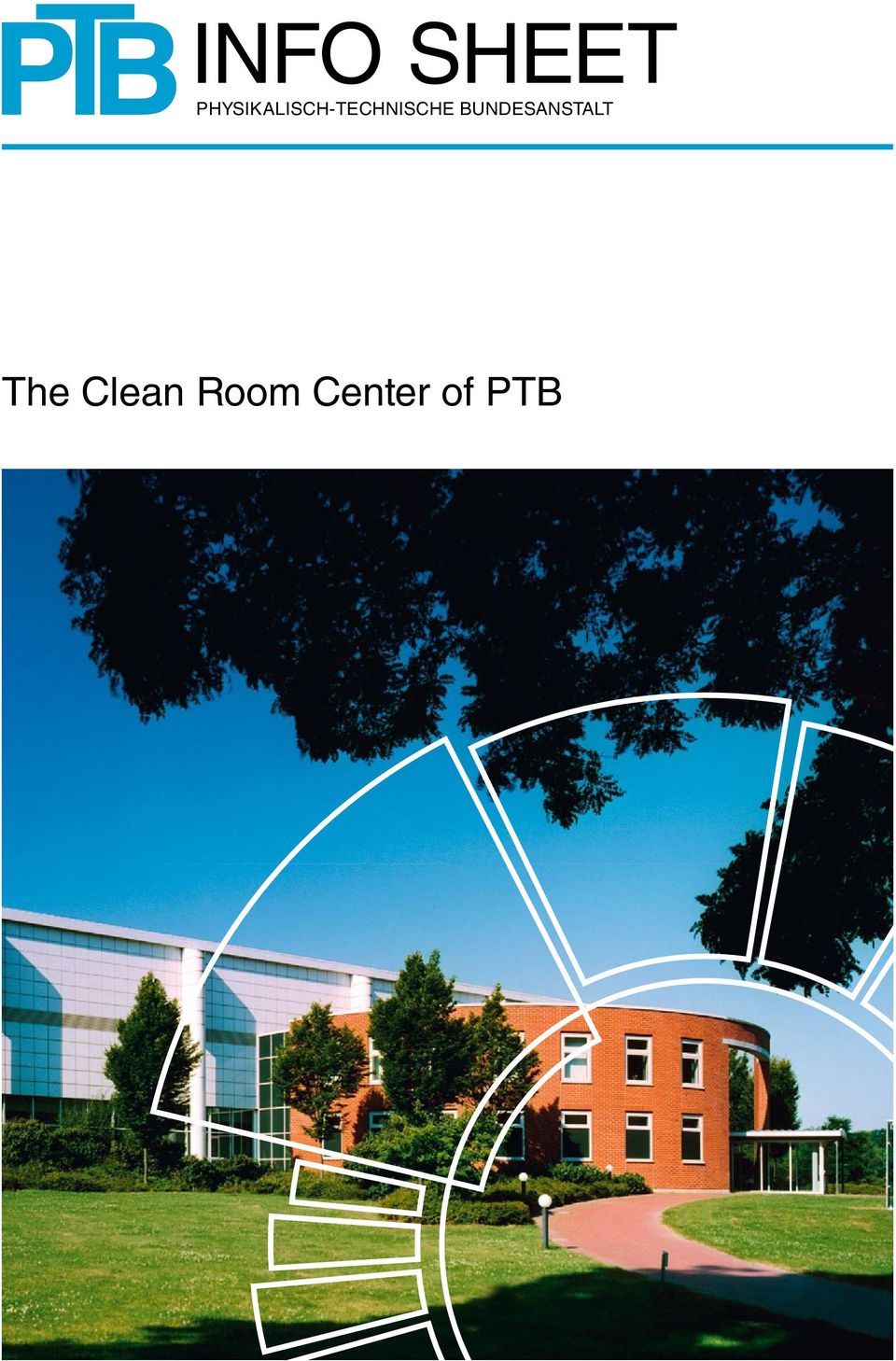
PHYSIKALISCH-TECHNISCHE BUNDESANSTALT. The Clean Room Center of PTB
|
|
|
- Maude Walsh
- 7 years ago
- Views:
Transcription
1 info sheet PHYSIKALISCH-TECHNISCHE BUNDESANSTALT The Clean Room Center of PTB
2 Clean Room Center The Clean Room Center of PTB is used to fabricate micro- and nanoelectronic circuits for electrical quantum metrology, to advance microand nanometrology, to perform ultra-precise angle and coordinate measurements, and to push the limits of optical metrology. Electrical precision measurements increasingly rely on the use of quantum standards whose precision is not limited by fabrication tolerances. Using quantum standards, electric units can be traced to the fundamental constants of nature, which are independent of time and space. Thus, quantum standards are universal gauges. Already today, the national metrology institutes use electrical quantum standards routinely to reproduce the units of voltage and resistance. Currently, quantum voltage and resistance standards are also being developed for industrial use. Quantum standards of the electric current are intensively investigated, driven by the intention of the Meter Convention to redefine the SI base unit ampere by linking it to the elementary charge. Quantum sensors, such as single-charge detectors and SQUIDs, are important measuring instruments due to their high sensitivity. The basis for all these metrological applications is laid by state-ofthe-art clean-room technology required for the fabrication of the micro- and nanoelectronic circuits that underpin today s electrical metrology. n Highly integrated Josephson Voltage Standards The Josephson voltage standard is the quantum standard for the representation of the volt. It consists of a series circuit of Josephson tunneling junctions which are fabricated by the deposition and patterning of superconducting thin films in the Clean Room Center. If a microwave is coupled into the Josephson junctions at low temperatures, quantized voltage steps are generated with values that only depend on fundamental constants and the frequency of the microwave. The quantized voltages have a relative uncertainty smaller than Series circuits with junctions for the generation of voltages of up to 10 V can be fabricated in the Clean Room Center. n Programmable Josephson voltage standard with junctions fabricated using SNS technology. The circuit generates an output voltage of 10 V. Quantum Hall Devices Quantum Hall devices are used to reproduce the unit of electrical resistance. The devices consist of a semiconductor hetero-structure fabricated by molecular beam epitaxy in the clean room centre. The two-dimensional electron gas in these structures shows quantized resistance values h / (ie 2 ) in high magnetic fields and at low temperatures (h Planck s constant, e elementary charge, i integer number). Resistance values can be reproduced with an uncertainty of approx in direct currents measurements. Moreover, if appropriate shielding is implemented, quantum Hall devices can also be used for highly precise ac measurements. Combined with optimized impedance bridges the unit of capacitance can be reproduced with an uncertainty below 10 8 using shielded quantum Hall devices. n Quantum Hall device.

3 Single-electron circuit with superconducting (S) leads and a normal conducting (N) charge island. Metallic single-electron Circuits The electric current can be linked to the elementary charge if single electrons are moved through a conductor in a controlled way. In the Clean Room Center, very small metallic tunneling junctions can be fabricated having sizes below 100 nm. At extremely low temperatures in the mk range, such structures exhibit the Coulomb blockade effect, which allows single electrons to be transferred at a selected frequency. By combining normal conductors and superconductors, unwanted transport processes can be suppressed to reduce the transfer error rate. n Semiconductor single-electron Pumps Semiconductor quantum circuits can be fabricated using molecular beam epitaxy and nanopatterning. Such circuits can be operated as single-electron pumps, in which an integer number of electrons is transferred in each cycle of a radiofrequency drive signal. Pumping operation can be realized at GHz frequencies generating comparatively large quantized currents in the na range. Semiconductor single-electron pumping is a promising concept for a scalable quantum standard of current. n Electron microscope image of a semiconductor single-electron pump: transport channel (colored green), gate electrodes (violet, yellow). Integrated Quantum Circuits Conventional measuring techniques are not able to determine the precision of single-electron transport in quantum circuits. Therefore, quantum sensors are used, which need to be integrated with single-electron sources on the same chip. If several single-electron sources are connected in series, the source of possible transfer errors can be identified. With the nanotechnology available in the Clean Room Center, integrated quantum circuits with several semiconductor single-electron pumps and metallic single-electron detectors can be fabricated. In order to increase the current, parallel circuits of singleelectron sources can be assembled. n Four semiconductor single-electron pumps connected in series. The charge transport is monitored by three single-electron detectors.

4 Reference Masks for Lithography The continuous miniaturization and increasing complexity of structures in the lithographical production process of highly integrated electronic components is a demanding challenge for the traceability of the dimensional measurements of such structures. This is particularly true for the characterization of structures on lithography masks. Calibrations of the widths and coordinates of structures on the masks require uncertainties in the nanometer range. With the help of PTB s electron optical metrology system (EOMS), e. g. calibrations of linewidth standards are performed for the mask industry. These measurements are refined by additional optical and scanning probe microscopy as well as by Monte Carlo simulations of the contrast of the EOMS signal at the line edges. n Optical Measurement Methods The ongoing quest for miniaturization in electronics, optics and mechanics requires an adequate measurement technology that is able to cope with the increasing challenges. Optical techniques for the dimensional measurement of structural parameters, e. g., width and pitch, have basic advantages because they are fast, contact-free and nondestructive. In the Clean Room Center, different optical measuring devices are provided, e. g., a UV microscope and an optical diffractometer, capable of performing dimensional measurements in the micrometer and submicrometer regimes. The sensitivity to contamination of the delicate samples requires the measurements to be performed in a clean room. n Layer Thickness and Surface Texture Metrology Surfaces of diamond-turned or super-polished metals, semiconductors and glass ceramics of, e. g., laser mirrors, wafer substrates and X-ray optics can be produced with nanometer surface roughness values. The measurement of such surfaces requires the application of three-dimensional measurement methods with improved lateral (area-based) and vertical resolution. In addition to standard interference microscopes, which allow the traceability to be realized to the unit of length, scanning-probe-based measurement methods and light-scatteringbased methods are applied. Furthermore, a spectroscopic ellipsometer with variable angle range is used for the calibration of layer thickness standards. For these calibrations, customers often require the work to be done under clean-room conditions. n Calibration of Micro- and Nanostructures Scanning probe microscopes have been established as important tools in different areas of nanotechnology. To use these instruments for purposes that go beyond mere imaging, i. e. as quantitative measurement instruments, a calibration of their scanning axes as well as exact knowledge of the effective interaction forces between the probe tip and the sample is necessary. In this context, different metrological scanning probe microscopes and special probe tips were developed which are operated in the Clean Room Center. Instruments of different designs and with different probing methods (contact and non-contact mode, probes for 2.5D and 3D probing) and scanning ranges are available. These measuring instruments are also increasingly applied for the calibration of standards which are necessary for quality control in production processes in micro- and nano-technology. On standards with high quality, uncertainties of U (k = 2) < 1 nm for step height calibrations for h = 2 µm and U (k = 2) < 10 pm for pitch calibrations can be obtained. n UV microscope for measurement of the structures on photo masks.

5 Coordinate Metrology For calibrations of the dimensions and form deviations of precision engineering components like, e. g., parts from fuel injection pumps, a high temperature stability and a close realization of the reference temperature for length measurements at 20 C is necessary. These conditions are available in the Clean Room Center. The reference standards are calibrated with small uncertainties and, in this way, make quality improvements in automobile supply industries feasible. Indirectly, they thus also contribute to a reduction of the CO 2 emissions in road traffic. Another important field of application is the dimensional calibration of primary standards like, e. g., piston-cylinder pressure standards. Dimensional measurements on prismatic and cylindrical standards can be realized with the measuring instruments operated in the Clean Room Center with the required measurement uncertainties. Many important standards are made of non-conducting and, thus, electrostatically sensitive materials. Measurements on these materials benefit in particular from the clean-room environment. n Precision Measurement of Optical Radiation In photometry and applied radiometry, one of the most urgent requests from customers is the simultaneous determination of the very different sensitivities of single-element and matrix detectors. This has to be accomplished by laser-based methods. The dust-free atmosphere of the Clean Room Center guarantees a perturbation-free, stable propagation of laser beams inside and outside of optical resonators, windows, lenses or the micrometer-sized surfaces of optical fibers used as lightguiding elements. The superb conditions are prerequisites for precision measurements of the optical radiative power and the generation of power-stabilized laser radiation fields. n Wavelength-tunable Ti:Sa laser with frequency doubling unit in the TULIP facility for the calibration of the irradiance-based sensitivity of photometers and radiometers in the short and long wavelength spectral region. Comparator MFU 110 for the precise determination of dimensional measurands on cylindrical standards. Angle Metrology For measurement and positioning tasks in precision manufacturing and in precision engineering, the reduction of the uncertainty for the determination of the plane angle is of increasing importance. Incremental angle measuring systems are the most accurate measuring systems applied for this purpose in industry. These systems, as well as the calibration of high-resolution electronic autocollimators, require measurements with highest accuracy. The precision angle comparator WMT 220 was installed for these tasks in the Clean Room Center and is applied for challenging calibration tasks, industrial cooperation projects and also for international comparison measurements. The comparator performance benefits from the very good temperature stability in the Clean Room Center and allows calibrations of arbitrary plane angles to be realized in the range up to 360 with uncertainties of only n Chip-scale Traps for Quantum Information and quantum-optical Precision Measurements Miniaturized traps for neutral atoms and single ions have found widespread application in the past few years, e. g. for quantum information processing, atom interferometry and for the investigation of novel quantum many-particle systems. In the framework of the Cluster of Excellence QUEST, chip scale traps are produced in the Clean Room Center which are used in the QUEST Institute at PTB and at the Leibniz Universität Hannover for the quantum information processing with single trapped ions. The metallic structures produced by means of optical lithography are distinguished by the integration of microwave conductive structures for the realization of novel control mechanisms for trapped ions. With the same technology, neutral atom chips are developed for atom-interferometric experiments at QUEST. n Test sample of an ion trap structure produced in the Clean Room Center. This structure has been devised by C. Ospelkaus at the National Institute of Science and Technology (NIST), USA, and is used here to characterize the fabrication process.

6 The Building Infrastructure and Contacts The Clean Room Center of PTB provides a well-suited environment with clean-room conditions, reduced mechanical vibrations, and a low audio noise level. The temperature and humidity are kept stable. The central clean room, 800 m 2 in size, can be divided in ten segments with different clean-room classes and environmental conditions. Central facilities have been established for the fabrication of micro- and nanostructures. Various electron beam and optical lithography systems exist, which allow direct writing of ultra-small structures and the writing of masks with feature sizes as small as 10 nm. Metal, semiconductor, and insulator thin films can be deposited, e. g., using a molecular beam epitaxy machine that allows the growth of ultra-clean semiconductor heterostructures. Lateral patterning is performed using various etching techniques. For the analysis of the micro- and nanostructures, high-resolution scanning electron and scanning force microscopes are available. The work in the Clean Room Center is performed in collaboration with universities, research institutes, other national metrology institutes, and industry partners located across Europe and around the globe. The joint work is funded by the European Union, the German federal government, the German National Science Foundation, the Volkswagen Foundation, and other national and international research funding organizations. The Clean Room Center is intensively used to carry out projects of the European Metrology Research Programme, in which national metrology institutes from Europe have joined forces to address the metrology needs of Europe in a coordinated effort. In the frame of PTB s mission, the Clean Room Center with its state-of-the-art technical infrastructure is available for joint work with external partners now and in the future. n Technical Infrastructure, basic Facts n Clean-room size 48 m x 17 m n Clean-room class 100 und 1000 n Air circulation 200/h n Average air velocity 20 cm/s n Temperature stability 0.1 K n Available temperature range 20 C to 23 C n Relative humidity 40 % to 55 % n Audio noise level < 45 db(a) n Oscillation amplitude of the clean-room floor < 0.3 μm for > 2 Hz < 0.5 μm for > 100 Hz Central Utilities n Ultra-clean water n Cooling water n Dust collection system n Handling vacuum n Ultra-clean gases n Ultra-clean aceton n Liquid nitrogen n Pressurized nitrogen n Ultra-clean pressurized air n Helium recovery n Emergency power supply Division 2: Electricity Head of Division: Dr. Uwe Siegner Phone: uwe.siegner@ptb.de Division 4: Optics Head of Division: Dr. Fritz Riehle Phone: fritz.riehle@ptb.de Division 5: Precision Engineering Head of Division: Dr. Harald Bosse Phone: harald.bosse@ptb.de Physikalisch-Technische Bundesanstalt Press and Information Office Bundesallee Braunschweig As of: March 2012

Physics 441/2: Transmission Electron Microscope
 Physics 441/2: Transmission Electron Microscope Introduction In this experiment we will explore the use of transmission electron microscopy (TEM) to take us into the world of ultrasmall structures. This
Quantum Computing for Beginners: Building Qubits
 Quantum Computing for Beginners: Building Qubits Suzanne Gildert Condensed Matter Physics Research (Quantum Devices Group) University of Birmingham 28/03/2007 Overview of this presentation What is a Qubit?
Calibration of AFM with virtual standards; robust, versatile and accurate. Richard Koops VSL Dutch Metrology Institute Delft
 Calibration of AFM with virtual standards; robust, versatile and accurate Richard Koops VSL Dutch Metrology Institute Delft 19-11-2015 VSL Dutch Metrology Institute VSL is the national metrology institute
3D TOPOGRAPHY & IMAGE OVERLAY OF PRINTED CIRCUIT BOARD ASSEMBLY
 3D TOPOGRAPHY & IMAGE OVERLAY OF PRINTED CIRCUIT BOARD ASSEMBLY Prepared by Duanjie Li, PhD & Andrea Novitsky 6 Morgan, Ste156, Irvine CA 92618 P: 949.461.9292 F: 949.461.9232 nanovea.com Today's standard
Quantum Metrology Closing the Quantum Triangle
 Quantum Metrology Closing the Quantum Triangle Quantum Triangle Heikki Seppä VTT Information Technology From Quantum Metrology into the Practical Applications MEG Printable Electronics Quantum Metrology
Nanometer-scale imaging and metrology, nano-fabrication with the Orion Helium Ion Microscope
 andras@nist.gov Nanometer-scale imaging and metrology, nano-fabrication with the Orion Helium Ion Microscope Bin Ming, András E. Vladár and Michael T. Postek National Institute of Standards and Technology
We know how to write nanometer. extreme lithography. extreme lithography. xlith Gesellschaft für Hochauflösende Lithografie Support & Consulting mbh
 extreme lithography extreme lithography xlith Gesellschaft für Hochauflösende Lithografie Support & Consulting mbh Wilhelm-Runge-Str. 11 89081 Ulm Germany phone +49 731 505 59 00 fax +49 731 505 59 05
Nanoscience Course Descriptions
 Nanoscience Course Descriptions NANO*1000 Introduction to Nanoscience This course introduces students to the emerging field of nanoscience. Its representation in popular culture and journalism will be
Experiment 5. Lasers and laser mode structure
 Northeastern University, PHYS5318 Spring 2014, 1 1. Introduction Experiment 5. Lasers and laser mode structure The laser is a very important optical tool that has found widespread use in science and industry,
Scanning Probe Microscopy
 Ernst Meyer Hans Josef Hug Roland Bennewitz Scanning Probe Microscopy The Lab on a Tip With 117 Figures Mß Springer Contents 1 Introduction to Scanning Probe Microscopy f f.1 Overview 2 f.2 Basic Concepts
Technology White Papers nr. 13 Paul Holister Cristina Román Vas Tim Harper
 QUANTUM DOTS Technology White Papers nr. 13 Paul Holister Cristina Román Vas Tim Harper QUANTUM DOTS Technology White Papers nr. 13 Release Date: Published by Científica Científica, Ltd. www.cientifica.com
UNIT I: INTRFERENCE & DIFFRACTION Div. B Div. D Div. F INTRFERENCE
 107002: EngineeringPhysics Teaching Scheme: Lectures: 4 Hrs/week Practicals-2 Hrs./week T.W.-25 marks Examination Scheme: Paper-50 marks (2 hrs) Online -50marks Prerequisite: Basics till 12 th Standard
MEMS mirror for low cost laser scanners. Ulrich Hofmann
 MEMS mirror for low cost laser scanners Ulrich Hofmann Outline Introduction Optical concept of the LIDAR laser scanner MEMS mirror requirements MEMS mirror concept, simulation and design fabrication process
The photoionization detector (PID) utilizes ultraviolet
 utilizes ultraviolet") Chapter 6 Photoionization Detectors The photoionization detector (PID) utilizes ultraviolet light to ionize gas molecules, and is commonly employed in the detection of volatile organic compounds (VOCs).
Chapter 6 Photoionization Detectors The photoionization detector (PID) utilizes ultraviolet light to ionize gas molecules, and is commonly employed in the detection of volatile organic compounds (VOCs).
Angle metrology at the PTB: current status and developments
 Angle metrology at the PTB: current status and developments M. Krause, A. Just, R. D. Geckeler, H. Bosse Physikalisch-Technische Bundesanstalt, Braunschweig und Berlin Bundesallee 100, D-38116 Braunschweig,
How to measure absolute pressure using piezoresistive sensing elements
 In sensor technology several different methods are used to measure pressure. It is usually differentiated between the measurement of relative, differential, and absolute pressure. The following article
Spectroscopy. Biogeochemical Methods OCN 633. Rebecca Briggs
 Spectroscopy Biogeochemical Methods OCN 633 Rebecca Briggs Definitions of Spectrometry Defined by the method used to prepare the sample 1. Optical spectrometry Elements are converted to gaseous atoms or
NUCLEAR MAGNETIC RESONANCE. Advanced Laboratory, Physics 407, University of Wisconsin Madison, Wisconsin 53706
 (revised 4/21/03) NUCLEAR MAGNETIC RESONANCE Advanced Laboratory, Physics 407, University of Wisconsin Madison, Wisconsin 53706 Abstract This experiment studies the Nuclear Magnetic Resonance of protons
Robert G. Hunsperger. Integrated Optics. Theory and Technology. Fourth Edition. With 195 Figures and 17 Tables. Springer
 Robert G. Hunsperger Integrated Optics Theory and Technology Fourth Edition With 195 Figures and 17 Tables Springer Contents 1. Introduction 1 1.1 Advantages of Integrated Optics 2 1.1.1 Comparison of
APPLICATION NOTE ULTRASONIC CERAMIC TRANSDUCERS
 APPLICATION NOTE ULTRASONIC CERAMIC TRANSDUCERS Selection and use of Ultrasonic Ceramic Transducers The purpose of this application note is to aid the user in the selection and application of the Ultrasonic
Encoders for Linear Motors in the Electronics Industry
 Technical Information Encoders for Linear Motors in the Electronics Industry The semiconductor industry and automation technology increasingly require more precise and faster machines in order to satisfy
Silicon-On-Glass MEMS. Design. Handbook
 Silicon-On-Glass MEMS Design Handbook A Process Module for a Multi-User Service Program A Michigan Nanofabrication Facility process at the University of Michigan March 2007 TABLE OF CONTENTS Chapter 1...
Development of New Inkjet Head Applying MEMS Technology and Thin Film Actuator
 Development of New Inkjet Head Applying MEMS Technology and Thin Film Actuator Kenji MAWATARI, Koich SAMESHIMA, Mitsuyoshi MIYAI, Shinya MATSUDA Abstract We developed a new inkjet head by applying MEMS
Near-field scanning optical microscopy (SNOM)
") Adviser: dr. Maja Remškar Institut Jožef Stefan January 2010 1 2 3 4 5 6 Fluorescence Raman and surface enhanced Raman 7 Conventional optical microscopy-limited resolution Two broad classes of techniques
Adviser: dr. Maja Remškar Institut Jožef Stefan January 2010 1 2 3 4 5 6 Fluorescence Raman and surface enhanced Raman 7 Conventional optical microscopy-limited resolution Two broad classes of techniques
1. INTRODUCTION ABSTRACT
 MultiWave Hybrid Laser Processing of Micrometer Scale Features for Flexible Electronics Applications J. Hillman, Y. Sukhman, D. Miller, M. Oropeza and C. Risser Universal Laser Systems, 7845 E. Paradise
MACHINE VISION FOR SMARTPHONES. Essential machine vision camera requirements to fulfill the needs of our society
 MACHINE VISION FOR SMARTPHONES Essential machine vision camera requirements to fulfill the needs of our society INTRODUCTION With changes in our society, there is an increased demand in stateof-the art
Development of certified reference material of thin film for thermal diffusivity
 Development of certified reference material of thin film for thermal diffusivity Takashi Yagi, Thermophysical properties section, NMIJ/AIST Joshua Martin MML, National Institute of Standards and Technology
Fiber Optics: Engineering from Global to Nanometer Dimensions
 Fiber Optics: Engineering from Global to Nanometer Dimensions Prof. Craig Armiento Fall 2003 1 Optical Fiber Communications What is it? Transmission of information using light over an optical fiber Why
Cross-beam scanning system to detect slim objects. 100 mm 3.937 in
 891 Object Area Sensor General terms and conditions... F-17 Related Information Glossary of terms... P.1359~ Sensor selection guide...p.831~ General precautions... P.1405 PHOTO PHOTO Conforming to EMC
ATOMIC SPECTRA. Apparatus: Optical spectrometer, spectral tubes, power supply, incandescent lamp, bottles of dyed water, elevating jack or block.
 1 ATOMIC SPECTRA Objective: To measure the wavelengths of visible light emitted by atomic hydrogen and verify the measured wavelengths against those predicted by quantum theory. To identify an unknown
1 Introduction. 1.1 Historical Perspective
 j1 1 Introduction 1.1 Historical Perspective The invention of scanning probe microscopy is considered one of the major advances in materials science since 1950 [1, 2]. Scanning probe microscopy includes
ENGINEERING METROLOGY
 ENGINEERING METROLOGY ACADEMIC YEAR 92-93, SEMESTER ONE COORDINATE MEASURING MACHINES OPTICAL MEASUREMENT SYSTEMS; DEPARTMENT OF MECHANICAL ENGINEERING ISFAHAN UNIVERSITY OF TECHNOLOGY Coordinate Measuring
Laboratory #3 Guide: Optical and Electrical Properties of Transparent Conductors -- September 23, 2014
 Laboratory #3 Guide: Optical and Electrical Properties of Transparent Conductors -- September 23, 2014 Introduction Following our previous lab exercises, you now have the skills and understanding to control
Lapping and Polishing Basics
 Lapping and Polishing Basics Applications Laboratory Report 54 Lapping and Polishing 1.0: Introduction Lapping and polishing is a process by which material is precisely removed from a workpiece (or specimen)
Acoustic GHz-Microscopy: Potential, Challenges and Applications
 Acoustic GHz-Microscopy: Potential, Challenges and Applications A Joint Development of PVA TePLa Analytical Systems GmbH and Fraunhofer IWM-Halle Dr. Sebastian Brand (Ph.D.) Fraunhofer CAM Fraunhofer Institute
Zero Width Glass Cutting with CO 2 Laser
 Zero Width Glass Cutting with CO 2 Laser Mohammed Naeem GSI Group, Laser Division Cosford Lane, Swift Valley Rugby mnaeem@gsig.com Introduction Laser cutting of glass in not a novel technique, excellent
Physical Science Study Guide Unit 7 Wave properties and behaviors, electromagnetic spectrum, Doppler Effect
 Objectives: PS-7.1 Physical Science Study Guide Unit 7 Wave properties and behaviors, electromagnetic spectrum, Doppler Effect Illustrate ways that the energy of waves is transferred by interaction with
Calibrating DC Shunts: Techniques and Uncertainties
 Calibrating DC Shunts: Techniques and Uncertainties Jay Klevens Ohm-Labs, Inc. 611 E. Carson St., Pittsburgh, PA 15203 (412) 431-0640 jklevens@ohm-labs.com Abstract Accurate electrical current measurement
Conductivity of silicon can be changed several orders of magnitude by introducing impurity atoms in silicon crystal lattice.
 CMOS Processing Technology Silicon: a semiconductor with resistance between that of conductor and an insulator. Conductivity of silicon can be changed several orders of magnitude by introducing impurity
Introduction to VLSI Fabrication Technologies. Emanuele Baravelli
 Introduction to VLSI Fabrication Technologies Emanuele Baravelli 27/09/2005 Organization Materials Used in VLSI Fabrication VLSI Fabrication Technologies Overview of Fabrication Methods Device simulation
METHODS FOR THE CALIBRATION OF ELECTROSTATIC MEASURING INSTRUMENTS
 METHODS FOR THE CALIBRATION OF ELECTROSTATIC MEASURING INSTRUMENTS Contents Foreword --------------------------------------------------------------------------------------------------------------------
SUPERCONDUCTIVITY. PH 318- Introduction to superconductors 1
 SUPERCONDUCTIVITY property of complete disappearance of electrical resistance in solids when they are cooled below a characteristic temperature. This temperature is called transition temperature or critical
Scanning Near Field Optical Microscopy: Principle, Instrumentation and Applications
 Scanning Near Field Optical Microscopy: Principle, Instrumentation and Applications Saulius Marcinkevičius Optics, ICT, KTH 1 Outline Optical near field. Principle of scanning near field optical microscope
PIEZOELECTRIC FILMS TECHNICAL INFORMATION
 PIEZOELECTRIC FILMS TECHNICAL INFORMATION 1 Table of Contents 1. PIEZOELECTRIC AND PYROELECTRIC EFFECTS 3 2. PIEZOELECTRIC FILMS 3 3. CHARACTERISTICS PROPERTIES OF PIEZOELECTRIC FILMS 3 4. PROPERTIES OF
Types of Epitaxy. Homoepitaxy. Heteroepitaxy
 Epitaxy Epitaxial Growth Epitaxy means the growth of a single crystal film on top of a crystalline substrate. For most thin film applications (hard and soft coatings, optical coatings, protective coatings)
High Voltage Power Supplies for Analytical Instrumentation
 ABSTRACT High Voltage Power Supplies for Analytical Instrumentation by Cliff Scapellati Power supply requirements for Analytical Instrumentation are as varied as the applications themselves. Power supply
Dew-Point Measurement Solutions
 Dew-Point Measurement Solutions www.michell.com Dew-Point Measurement Solutions Special Features No downtime Michell Instruments offers a unique sensor exchange programme, which means that you will never
Development of Ultra-Multilayer. printed circuit board
 Development of Ultra-Multilayer Printed Circuit Board Yasuyuki Shinbo Using the multilayer and characteristic impedance control technologies cultivated in the field of telecommunications, OKI Printed Circuits
ECP Embedded Component Packaging Technology
 ECP Embedded Component Packaging Technology A.Kriechbaum, H.Stahr, M.Biribauer, N.Haslebner, M.Morianz AT&S Austria Technologie und Systemtechnik AG Abstract The packaging market has undergone tremendous
CHAPTER - 1. Chapter ONE: WAVES CHAPTER - 2. Chapter TWO: RAY OPTICS AND OPTICAL INSTRUMENTS. CHAPTER - 3 Chapter THREE: WAVE OPTICS PERIODS PERIODS
 BOARD OF INTERMEDIATE EDUCATION, A.P., HYDERABAD REVISION OF SYLLABUS Subject PHYSICS-II (w.e.f 2013-14) Chapter ONE: WAVES CHAPTER - 1 1.1 INTRODUCTION 1.2 Transverse and longitudinal waves 1.3 Displacement
Welcome to this presentation on LED System Design, part of OSRAM Opto Semiconductors LED 101 series.
 Welcome to this presentation on LED System Design, part of OSRAM Opto Semiconductors LED 101 series. 1 To discuss the design challenges of LED systems we look at the individual system components. A basic
Injection moulding and modelling on a micro scale
 Injection moulding and modelling on a micro scale Technology Update Injection moulding and welding of plastics 11 November 2014 Research Projects (National / European) Micro/Nano/Multimaterial Manufacturing
Coating Thickness and Composition Analysis by Micro-EDXRF
 Application Note: XRF Coating Thickness and Composition Analysis by Micro-EDXRF www.edax.com Coating Thickness and Composition Analysis by Micro-EDXRF Introduction: The use of coatings in the modern manufacturing
Hello and Welcome to this presentation on LED Basics. In this presentation we will look at a few topics in semiconductor lighting such as light
 Hello and Welcome to this presentation on LED Basics. In this presentation we will look at a few topics in semiconductor lighting such as light generation from a semiconductor material, LED chip technology,
Nanoscale Resolution Options for Optical Localization Techniques. C. Boit TU Berlin Chair of Semiconductor Devices
 berlin Nanoscale Resolution Options for Optical Localization Techniques C. Boit TU Berlin Chair of Semiconductor Devices EUFANET Workshop on Optical Localization Techniques Toulouse, Jan 26, 2009 Jan 26,
It has long been a goal to achieve higher spatial resolution in optical imaging and
 Nano-optical Imaging using Scattering Scanning Near-field Optical Microscopy Fehmi Yasin, Advisor: Dr. Markus Raschke, Post-doc: Dr. Gregory Andreev, Graduate Student: Benjamin Pollard Department of Physics,
Metrology Standards for Semiconductor Manufacturing Yu Guan and Marco Tortonese VLSI Standards, Inc., 3087 North First Street, San Jose, CA 95134, USA
 Metrology Standards for Semiconductor Manufacturing Yu Guan and Marco Tortonese VLSI Standards, Inc., 3087 North First Street, San Jose, CA 95134, USA Abstract In semiconductor manufacturing, the performance
A METHOD OF PRECISE CALIBRATION FOR PIEZOELECTRICAL ACTUATORS
 Uludağ Üniversitesi Mühendislik-Mimarlık Fakültesi Dergisi, Cilt 9, Sayı, 24 A METHOD OF PRECISE CALIBRATION FOR PIEZOELECTRICAL ACTUATORS Timur CANEL * Yüksel BEKTÖRE ** Abstract: Piezoelectrical actuators
Coating Technology: Evaporation Vs Sputtering
 Satisloh Italy S.r.l. Coating Technology: Evaporation Vs Sputtering Gianni Monaco, PhD R&D project manager, Satisloh Italy 04.04.2016 V1 The aim of this document is to provide basic technical information
SpeedLight 2D. for efficient production of printed circuit boards
 laser direct imaging SpeedLight 2D laser direct imaging platform for efficient production of printed circuit boards MANZ AG /// Manz SpeedLight 2D /// 2 History of the development of Manz SpeedLight 2D
Plastic Film Texture Measurement With 3D Profilometry
 Plastic Film Texture Measurement With 3D Profilometry Prepared by Jorge Ramirez 6 Morgan, Ste156, Irvine CA 92618 P: 949.461.9292 F: 949.461.9232 nanovea.com Today's standard for tomorrow's materials.
ME 472 Engineering Metrology
 ME 472 Engineering Metrology and Quality Control Chp 6 - Advanced Measurement Systems Mechanical Engineering University of Gaziantep Dr. A. Tolga Bozdana Assistant Professor Coordinate Measuring Machines
14.5GHZ 2.2KW CW GENERATOR. GKP 22KP 14.5GHz WR62 3x400V
 14.5GHZ 2.2KW CW GENERATOR GKP 22KP 14.5GHz WR62 3x400V UTILIZATION OF GKP 22KP GENERATOR With its characteristics of power stability whatever the load, very fast response time at a pulse, low ripple,
Temperature. LumaSense Technologies, Inc. supplies a unique selection of very precise calibration
 Temperature Calibration Sources Highly accurate calibration equipment for pyrometers, thermal imaging cameras, radiometers, heatflux and spectrographic measurement sytems. Calibration sources are infrared
Usage of Carbon Nanotubes in Scanning Probe Microscopes as Probe. Keywords: Carbon Nanotube, Scanning Probe Microscope
 International Journal of Arts and Sciences 3(1): 18-26 (2009) CD-ROM. ISSN: 1944-6934 InternationalJournal.org Usage of Carbon Nanotubes in Scanning Probe Microscopes as Probe Bedri Onur Kucukyildirim,
Micro-CT for SEM Non-destructive Measurement and Volume Visualization of Specimens Internal Microstructure in SEM Micro-CT Innovation with Integrity
 Micro-CT for SEM Non-destructive Measurement and Volume Visualization of Specimens Internal Microstructure in SEM Innovation with Integrity Micro-CT 3D Microscopy Using Micro-CT for SEM Micro-CT for SEM
A receiver TDC chip set for accurate pulsed time-of-flight laser ranging
 A receiver TDC chip set for accurate pulsed time-of-flight laser ranging Juha Kostamovaara, Sami Kurtti, Jussi-Pekka Jansson University of Oulu, Department of Electrical Engineering, Electronics Laboratory,
Introduction to Fourier Transform Infrared Spectrometry
 Introduction to Fourier Transform Infrared Spectrometry What is FT-IR? I N T R O D U C T I O N FT-IR stands for Fourier Transform InfraRed, the preferred method of infrared spectroscopy. In infrared spectroscopy,
Optical Methods of Surface Measurement
 Optical Methods of Surface Measurement Ted Vorburger, Guest Researcher National Institute of Standards and Technology (NIST) Measurement Science and Standards in Forensic Firearms Analysis 2012 NIST, Gaithersburg,
PHYSICS PAPER 1 (THEORY)
") PHYSICS PAPER 1 (THEORY) (Three hours) (Candidates are allowed additional 15 minutes for only reading the paper. They must NOT start writing during this time.) ---------------------------------------------------------------------------------------------------------------------
PHYSICS PAPER 1 (THEORY) (Three hours) (Candidates are allowed additional 15 minutes for only reading the paper. They must NOT start writing during this time.) ---------------------------------------------------------------------------------------------------------------------
Nano-Spectroscopy. Solutions AFM-Raman, TERS, NSOM Chemical imaging at the nanoscale
 Nano-Spectroscopy Solutions AFM-Raman, TERS, NSOM Chemical imaging at the nanoscale Since its introduction in the early 80 s, Scanning Probe Microscopy (SPM) has quickly made nanoscale imaging an affordable
MICRO DROPLET GENERATION TECHNOLOGY
 MICRO DROPLET GENERATION TECHNOLOGY Micro-droplet Generation Technology Micro-droplet Generation System Semiconductor Wafer Cleaning Precision Coating Emulsion Twin-Fluid Nozzle System www.hshi-tech.co.kr
EMI in Electric Vehicles
 EMI in Electric Vehicles S. Guttowski, S. Weber, E. Hoene, W. John, H. Reichl Fraunhofer Institute for Reliability and Microintegration Gustav-Meyer-Allee 25, 13355 Berlin, Germany Phone: ++49(0)3046403144,
Micro-Power Generation
 Micro-Power Generation Elizabeth K. Reilly February 21, 2007 TAC-meeting 1 Energy Scavenging for Wireless Sensors Enabling Wireless Sensor Networks: Ambient energy source Piezoelectric transducer technology
Advanced VLSI Design CMOS Processing Technology
 Isolation of transistors, i.e., their source and drains, from other transistors is needed to reduce electrical interactions between them. For technologies
Nano Optics: Overview of Research Activities. Sergey I. Bozhevolnyi SENSE, University of Southern Denmark, Odense, DENMARK
 Nano Optics: Overview of Research Activities SENSE, University of Southern Denmark, Odense, DENMARK Optical characterization techniques: Leakage Radiation Microscopy Scanning Near-Field Optical Microscopy
5. Scanning Near-Field Optical Microscopy 5.1. Resolution of conventional optical microscopy
 5. Scanning Near-Field Optical Microscopy 5.1. Resolution of conventional optical microscopy Resolution of optical microscope is limited by diffraction. Light going through an aperture makes diffraction
Miniaturizing Flexible Circuits for use in Medical Electronics. Nate Kreutter 3M
 Miniaturizing Flexible Circuits for use in Medical Electronics Nate Kreutter 3M Drivers for Medical Miniaturization Market Drivers for Increased use of Medical Electronics Aging Population Early Detection
Final Publishable JRP Summary Report for JRP ENG06 Power Plants Metrology for improved power plant efficiency
 Final Report for JRP Metrology for improved power plant efficiency Overview: Large scale power plants based on nuclear or conventional fuel provide about 80 % of generated electricity in the EU and nearly
ALD Atomic Layer Deposition
 Research - Services ALD Atomic Layer Deposition Atomic Layer Deposition is a deposition process for assembling of thin films on the nanometer scale. The self-limiting deposition of atomic monolayers occurs
Fiber optic communication
 Fiber optic communication Fiber optic communication Outline Introduction Properties of single- and multi-mode fiber Optical fiber manufacture Optical network concepts Robert R. McLeod, University of Colorado
Lecture 4 Scanning Probe Microscopy (SPM)
") Lecture 4 Scanning Probe Microscopy (SPM) General components of SPM; Tip --- the probe; Cantilever --- the indicator of the tip; Tip-sample interaction --- the feedback system; Scanner --- piezoelectric
Lecture 4 Scanning Probe Microscopy (SPM) General components of SPM; Tip --- the probe; Cantilever --- the indicator of the tip; Tip-sample interaction --- the feedback system; Scanner --- piezoelectric
Demonstration of sub-4 nm nanoimprint lithography using a template fabricated by helium ion beam lithography
 Demonstration of sub-4 nm nanoimprint lithography using a template fabricated by helium ion beam lithography Wen-Di Li*, Wei Wu** and R. Stanley Williams Hewlett-Packard Labs *Current address: University
Connectivity in a Wireless World. Cables Connectors 2014. A Special Supplement to
 Connectivity in a Wireless World Cables Connectors 204 A Special Supplement to Signal Launch Methods for RF/Microwave PCBs John Coonrod Rogers Corp., Chandler, AZ COAX CABLE MICROSTRIP TRANSMISSION LINE
BARE PCB INSPECTION BY MEAN OF ECT TECHNIQUE WITH SPIN-VALVE GMR SENSOR
 BARE PCB INSPECTION BY MEAN OF ECT TECHNIQUE WITH SPIN-VALVE GMR SENSOR K. Chomsuwan 1, S. Yamada 1, M. Iwahara 1, H. Wakiwaka 2, T. Taniguchi 3, and S. Shoji 4 1 Kanazawa University, Kanazawa, Japan;
E. K. A. ADVANCED PHYSICS LABORATORY PHYSICS 3081, 4051 NUCLEAR MAGNETIC RESONANCE
 E. K. A. ADVANCED PHYSICS LABORATORY PHYSICS 3081, 4051 NUCLEAR MAGNETIC RESONANCE References for Nuclear Magnetic Resonance 1. Slichter, Principles of Magnetic Resonance, Harper and Row, 1963. chapter
Nano Meter Stepping Drive of Surface Acoustic Wave Motor
 Proc. of 1st IEEE Conf. on Nanotechnology, Oct. 28-3, pp. 495-5, (21) Maui, Hawaii Nano Meter Stepping Drive of Surface Acoustic Wave Motor Takashi Shigematsu*, Minoru Kuribayashi Kurosawa*, and Katsuhiko
Synthetic Sensing: Proximity / Distance Sensors
 Synthetic Sensing: Proximity / Distance Sensors MediaRobotics Lab, February 2010 Proximity detection is dependent on the object of interest. One size does not fit all For non-contact distance measurement,
ELECTRIC FIELD LINES AND EQUIPOTENTIAL SURFACES
 ELECTRIC FIELD LINES AND EQUIPOTENTIAL SURFACES The purpose of this lab session is to experimentally investigate the relation between electric field lines of force and equipotential surfaces in two dimensions.
ELECTRON SPIN RESONANCE Last Revised: July 2007
 QUESTION TO BE INVESTIGATED ELECTRON SPIN RESONANCE Last Revised: July 2007 How can we measure the Landé g factor for the free electron in DPPH as predicted by quantum mechanics? INTRODUCTION Electron
EASIDEW PORTABLE HYGROMETER INSTALLATION, OPERATION AND MAINTENANCE MANUAL
 EASIDEW PORTABLE HYGROMETER INSTALLATION, OPERATION AND MAINTENANCE MANUAL Issue February 2004 2 TABLE OF CONTENTS SECTION PAGE 1. INTRODUCTION 3 1.1 General 3 1.2 Ceramic Sensing Element 3 1.3 Calibration
Neuere Entwicklungen zur Herstellung optischer Schichten durch reaktive. Wolfgang Hentsch, Dr. Reinhard Fendler. FHR Anlagenbau GmbH
 Neuere Entwicklungen zur Herstellung optischer Schichten durch reaktive Sputtertechnologien Wolfgang Hentsch, Dr. Reinhard Fendler FHR Anlagenbau GmbH Germany Contents: 1. FHR Anlagenbau GmbH in Brief
Applications and Benefits of Multi-Walled Carbon Nanotubes (MWCNT)
") I Applications and Benefits of Multi-Walled Carbon Nanotubes (MWCNT) Table of Content 1 Introduction...1 2 Improved Properties...1 3 Potential Applications...1 3.1 Current / short-term applications...3
I Applications and Benefits of Multi-Walled Carbon Nanotubes (MWCNT) Table of Content 1 Introduction...1 2 Improved Properties...1 3 Potential Applications...1 3.1 Current / short-term applications...3
EMC STANDARDS STANDARDS AND STANDARD MAKING BODIES. International. International Electrotechnical Commission (IEC) http://www.iec.
 http://www.iec.") EMC STANDARDS The EMC standards that a particular electronic product must meet depend on the product application (commercial or military) and the country in which the product is to be used. These EMC regulatory
EMC STANDARDS The EMC standards that a particular electronic product must meet depend on the product application (commercial or military) and the country in which the product is to be used. These EMC regulatory
Advancements in High Frequency, High Resolution Acoustic Micro Imaging for Thin Silicon Applications
 Advancements in High Frequency, High Resolution Acoustic Micro Imaging for Thin Silicon Applications Janet E. Semmens Sonoscan, Inc. 2149 E. Pratt Boulevard Elk Grove Village, IL 60007 USA Phone: (847)
CREOL, College of Optics & Photonics, University of Central Florida
 OSE6650 - Optical Properties of Nanostructured Materials Optical Properties of Nanostructured Materials Fall 2013 Class 3 slide 1 Challenge: excite and detect the near field Thus far: Nanostructured materials
Spectral Measurement Solutions for Industry and Research
 Spectral Measurement Solutions for Industry and Research Hamamatsu Photonics offers a comprehensive range of products for spectroscopic applications, covering the, Visible and Infrared regions for Industrial,
h e l p s y o u C O N T R O L
 contamination analysis for compound semiconductors ANALYTICAL SERVICES B u r i e d d e f e c t s, E v a n s A n a l y t i c a l g r o u p h e l p s y o u C O N T R O L C O N T A M I N A T I O N Contamination
High Rate Oxide Deposition onto Web by Reactive Sputtering from Rotatable Magnetrons
 High Rate Oxide Deposition onto Web by Reactive Sputtering from Rotatable Magnetrons D.Monaghan, V. Bellido-Gonzalez, M. Audronis. B. Daniel Gencoa, Physics Rd, Liverpool, L24 9HP, UK. www.gencoa.com,
Tube Control Measurement, Sorting Modular System for Glass Tube
 Tube Control Measurement, Sorting Modular System for Glass Tube Tube Control is a modular designed system of settled instruments and modules. It comprises measuring instruments for the tube dimensions,