AUDIO DIFFERENTIAL LINE RECEIVER. 0dB (G = 1)
|
|
|
- Marcia Jacobs
- 7 years ago
- Views:
Transcription
1 INA4 INA4 INA4 INA4 INA4 INA4 AUDIO DIFFERENTIAL LINE RECEIVERS db (G = ) FEATURES SINGLE AND DUAL VERSIONS LOW DISTORTION:.% at f = khz HIGH SLEW RATE: 4V/µs FAST SETTLING TIME: µs to.% WIDE SUPPLY RANGE: ±4V to ±8V LOW QUIESCENT CURRENT:.9mA max HIGH CMRR: 9dB FIXED GAIN = db (V/V) PACKAGES SINGLE: 8-PIN DIP, SO-8 DESCRIPTION DUAL: 4-PIN DIP, SO-4 The INA4 and INA4 are differential line receivers consisting of high performance op amps with onchip precision resistors. They are fully specified for high performance audio applications and have excellent ac specifications, including low distortion (.% at khz) and high slew rate (4V/µs), assuring good dynamic response. In addition, wide output voltage swing and high output drive capability allow use in a wide variety of demanding applications. The dual version features completely independent circuitry for lowest crosstalk and freedom from interaction, even when overdriven or overloaded. The INA4 and INA4 on-chip resistors are laser trimmed for accurate gain and optimum common-mode rejection. Furthermore, excellent TCR tracking of the resistors maintains gain accuracy and common-mode rejection over temperature. Operation is guaranteed from ±4V to ±8V (8V to V total supply). The INA4 is available in 8-pin DIP and SO-8 surface-mount packages. The INA4 comes in 4-pin DIP and SO-4 surface-mount packages. Both are specified for operation over the extended industrial temperature range, 4 C to +8 C. APPLICATIONS AUDIO DIFFERENTIAL LINE RECEIVER SUMMING AMPLIFIER UNITY-GAIN INVERTING AMPLIFIER PSUEDOGROUND GENERATOR INSTRUMENTATION BUILDING BLOCK CURRENT SHUNT MONITOR VOLTAGE-CONTROLLED CURRENT SOURCE GROUND LOOP ELIMINATOR In +In 7 4 V+ V INA4 In A +In A In B +In B Sense Output Ref 4 V+ A B INA Sense A Out A Ref A Sense B Out B Ref B International Airport Industrial Park Mailing Address: PO Box 4, Tucson, AZ 874 Street Address: 7 S. Tucson Blvd., Tucson, AZ 87 Tel: () 74- Twx: 9-9- Internet: FAXLine: (8) 48- (US/Canada Only) Cable: BBRCORP Telex: -49 FAX: () 889- Immediate Product Info: (8) 48- V SBOS7 997 Burr-Brown Corporation PDS-9A Printed in U.S.A. July, 997

2 SPECIFICATIONS: V S = ±8V At T A = + C, V S = ±8V, R L = kω, and Ref Pin connected to Ground, unless otherwise noted. INA4PA, UA INA4PA, UA PARAMETER CONDITIONS MIN TYP MAX UNITS AUDIO PERFORMANCE Total Harmonic Distortion + Noise, f = khz V IN = Vrms. % Noise Floor () khz BW dbu Headroom () THD+N < % + dbu FREQUENCY RESPONSE Small-Signal Bandwidth. MHz Slew Rate 4 V/µs Settling Time:.% V Step, C L = pf µs.% V Step, C L = pf µs Overload Recovery Time % Overdrive µs Channel Separation (dual), f = khz 7 db OUTPUT NOISE VOLTAGE () f = Hz to khz 7 µvrms f = khz nv/ HZ OFFSET VOLTAGE () Input Offset Voltage V CM = V ± ± µv vs Temperature Specified Temperature Range ± µv/ C vs Power Supply V S = ±4V to ±8V ± ± µv/v INPUT Common-Mode Voltage Range: Positive V O = V (V+) (V+) 4 V Negative V O = V (V )+ (V )+ V Differential Voltage Range See Typical Curve Common-Mode Rejection V CM = ±V, R S = Ω 74 9 db Impedance (4) Differential kω Common-Mode kω GAIN Initial V/V Error V O = V to V ±. ±. % vs Temperature ± ± ppm/ C Nonlinearity V O = V to V. % OUTPUT Voltage Output, Positive (V+) (V+).8 V Negative (V )+ (V )+. V Current Limit, Continuous to Common ± ma Capacitive Load (Stable Operation) pf POWER SUPPLY Rated Voltage ±8 V Voltage Range ±4 ±8 V Quiescent Current (per Amplifier) I O = ±.4 ±.9 ma TEMPERATURE RANGE Specification Range 4 8 C Operation Range C Storage Range C Thermal Resistance, θ JA 8-Pin DIP C/W SO-8 Surface-Mount C/W 4-Pin DIP 8 C/W SO-4 Surface-Mount C/W NOTES: () dbu = log (Vrms/.774). () Includes effects of amplifier s input current noise and thermal noise contribution of resistor network. () Includes effects of amplifier s input bias and offset currents. (4) resistors are ratio matched but have ±% absolute value. The information provided herein is believed to be reliable; however, BURR-BROWN assumes no responsibility for inaccuracies or omissions. BURR-BROWN assumes no responsibility for the use of this information, and all use of such information shall be entirely at the user s own risk. Prices and specifications are subject to change without notice. No patent rights or licenses to any of the circuits described herein are implied or granted to any third party. BURR-BROWN does not authorize or warrant any BURR-BROWN product for use in life support devices and/or systems. INA4/4
, f = khz 7 db OUTPUT NOISE VOLTAGE () f = Hz to khz 7 µvrms f = khz nv/ HZ OFFSET VOLTAGE () Input Offset Voltage")
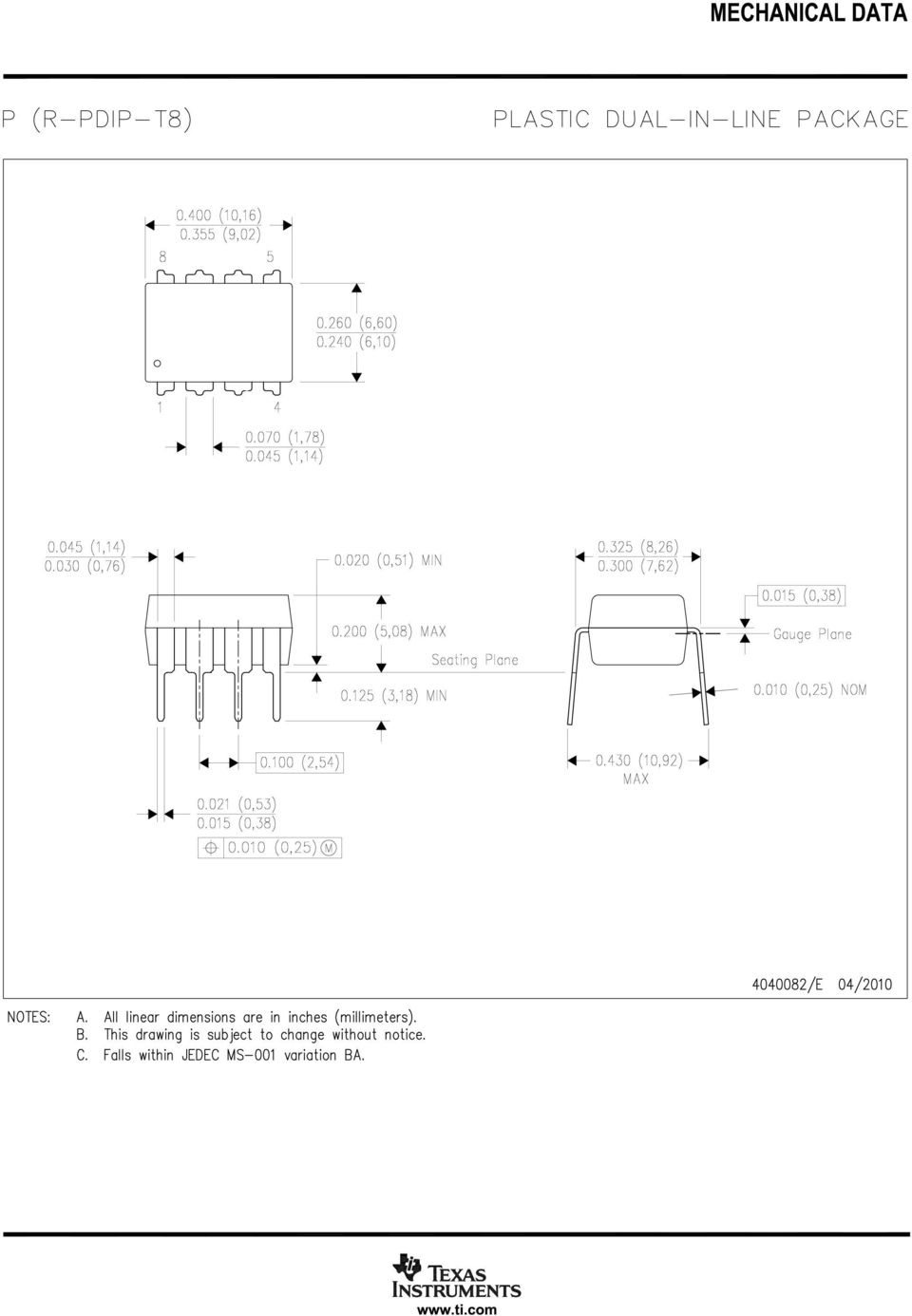
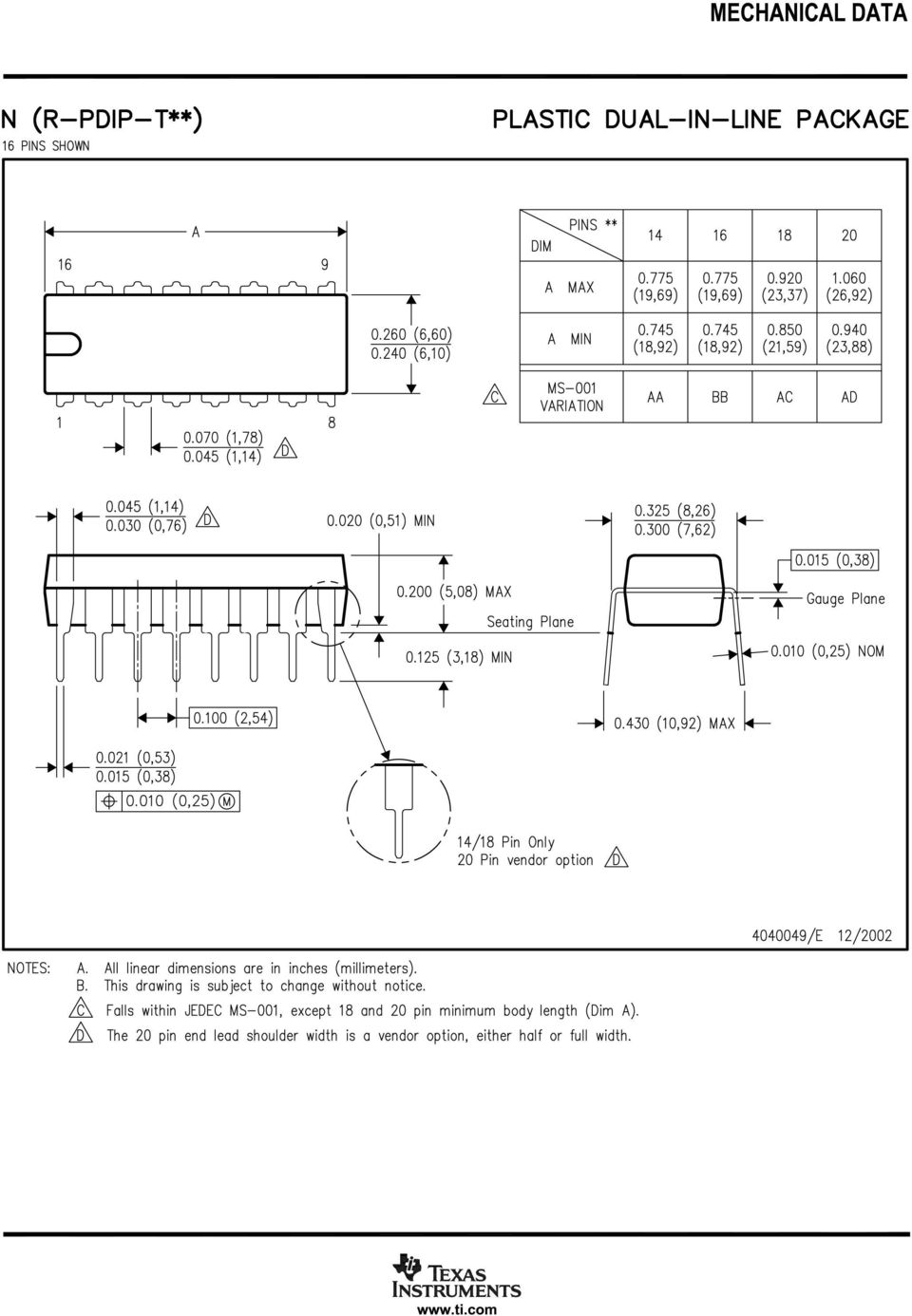
3 PIN CONFIGURATIONS Top View 8-Pin DIP/SO-8 Top View 4-Pin DIP/SO-4 Ref 8 NC NC 4 Ref A In 7 V+ In A A Out A +In Output +In A Sense A V 4 Sense V 4 V+ NC = No Connection +In B B Sense B In B 9 Out B ABSOLUTE MAXIMUM RATINGS () NC 7 8 Ref B Supply Voltage, V+ to V... 4V Input Voltage Range... ±8V Output Short-Circuit (to ground) ()... Continuous Operating Temperature... C to + C Storage Temperature... C to + C Junction Temperature... + C Lead Temperature (soldering, s)... + C NOTE: () Stresses above these ratings may cause permanent damage. () One channel per package. PACKAGE/ORDERING INFORMATION PACKAGE SPECIFICATION DRAWING TEMPERATURE PRODUCT PACKAGE NUMBER () RANGE Single INA4PA 8-Pin DIP 4 C to +8 C INA4UA SO-8 Surface-Mount 8 4 C to +8 C Dual INA4PA 4-Pin DIP 4 C to +8 C INA4UA SO-4 Surface-Mount 4 C to +8 C NOTE: () For detailed drawing and dimension table, please see end of data sheet, or Appendix C of Burr-Brown IC Data Book. NC = No Connection ELECTROSTATIC DISCHARGE SENSITIVITY This integrated circuit can be damaged by ESD. Burr-Brown recommends that all integrated circuits be handled with appropriate precautions. Failure to observe proper handling and installation procedures can cause damage. ESD damage can range from subtle performance degradation to complete device failure. Precision integrated circuits may be more susceptible to damage because very small parametric changes could cause the device not to meet its published specifications. INA4/4
 RANGE Single INA4PA 8-Pin DIP 4 C to +8 C INA4UA SO-8 Surface-Mount 8 4 C to +8 C Dual INA4PA 4-Pin")
4 TYPICAL PERFORMANCE CURVES At T A = + C, V S = ±8V, unless otherwise noted. TOTAL HARMONIC DISTORTION+NOISE vs FREQUENCY V O = Vrms DIM INTERMODULATION DISTORTION vs OUTPUT AMPLITUDE BW = khz. THD+Noise (%).. R L = kω R L = kω DIM (%).. R L = kω, Ω R L = Ω. k k k Frequency (Hz). Output Amplitude (dbu) HEADROOM - TOTAL HARMONIC DISTORTION+NOISE vs OUTPUT AMPLITUDE. HARMONIC DISTORTION PRODUCTS vs FREQUENCY THD+Noise (%)... f = khz R L = Ω Output Amplitude (dbu) R L = kω, kω. Amplitude (% of Fundamental)... R L = Ω, nd Harmonic R L = kω, rd Harmonic R L = kω, nd Harmonic V O = Vrms. k k k Frequency (Hz) R L = Ω, rd Harmonic ( noise limited) k OUTPUT VOLTAGE NOISE SPECTRAL DENSITY vs FREQUENCY OUTPUT NOISE VOLTAGE vs NOISE BANDWIDTH Voltage Noise (nv/ Hz) k Noise Voltage (µvrms) k k k M Frequency (Hz). k k k Frequency (Hz) INA4/4 4

5 TYPICAL PERFORMANCE CURVES (CONT) At T A = + C, V S = ±8V, unless otherwise noted. GAIN vs FREQUENCY COMMON-MODE REJECTION vs FREQUENCY Voltage Gain (db) Common-Mode Rejection (db) 8 4 k k k M M Frequency (Hz) k k k M Frequency (Hz) POWER SUPPLY REJECTION vs FREQUENCY CHANNEL SEPARATION vs FREQUENCY Power Supply Rejection (db) 8 4 +PSR PSR Channel Separation (db) R L = kω R L = kω k k k M Frequency (Hz) 9 k k k Frequency (Hz) Output Voltage (Vp-p) MAXIMUM OUTPUT VOLTAGE vs FREQUENCY 4 k k k M M Frequency (Hz) Common-Mode Voltage (V) 4 INPUT COMMON-MODE VOLTAGE RANGE vs OUTPUT VOLTAGE V 4 REF = V R L = kω Output Voltage (V) V S = ±8V INA4/4
 9 k k k Frequency (Hz) Output Voltage (Vp-p) MAXIMUM OUTPUT VOLTAGE vs FREQUENCY 4 k k k M M Frequency (Hz) Common-Mode Voltage (V) 4 INPUT")
6 TYPICAL PERFORMANCE CURVES (CONT) At T A = + C, V S = ±8V, unless otherwise noted. 4 QUIESCENT CURRENT vs TEMPERATURE SLEW RATE vs TEMPERATURE Quiescent Current (ma) Slew Rate (V/µs) 4 SR +SR 7 7 Temperature ( C) Temperature ( C) 8 SHORT-CIRCUIT CURRENT vs TEMPERATURE QUIESCENT CURRENT vs SUPPLY VOLTAGE Short-Circuit Current (ma) 4 4 I SC +I SC Quiescent Current (ma) Temperature ( C) ±4 ± ±8 ± ± ±4 ± ±8 Supply Voltage (V) Percent of Amplifiers (%) Typical Production Distribution of Packaged Units. OFFSET VOLTAGE PRODUCTION DISTRIBUTION Percent of Amplifiers (%) OFFSET VOLTAGE DRIFT PRODUCTION DISTRIBUTION Typical Production Distribution of Packaged Units Offset Voltage (µv) Offset Voltage Drift (µv/ C) INA4/4

7 TYPICAL PERFORMANCE CURVES (CONT) At T A = + C, V S = ±8V, unless otherwise noted. Output Voltage Swing (V) OUTPUT VOLTAGE SWING vs OUTPUT CURRENT 7 C 4 C C 8 C 4 C 8 C C C 7 ± ±4 ± ±8 ± Output Current (ma) Overshoot (%) 7 4 SMALL-SIGNAL OVERSHOOT vs LOAD CAPACITANCE 4 8 Load Capacitance (pf) R L = kω mv Step SMALL-SIGNAL STEP RESPONSE LARGE-SIGNAL STEP RESPONSE C L = pf C L = pf mv/div V/div C L = pf µs/div µs/div 7 INA4/4

8 APPLICATIONS INFORMATION Figure shows the basic connections required for operation of the INA4. Decoupling capacitors are strongly recommended in applications with noisy or high impedance power supplies. The capacitors should be placed close to the device pins as shown in Figure. All circuitry is completely independent in the dual version assuring lowest crosstalk and normal behavior when one amplifier is overdriven or short-circuited. As shown in Figure, the differential input signal is connected to pins and. The source impedances connected to the inputs must be nearly equal to assure good commonmode rejection. A Ω mismatch in source impedance will degrade the common-mode rejection of a typical device to approximately 74dB. If the source has a known impedance mismatch, an additional resistor in series with the opposite input can be used to preserve good common-mode rejection. Do not interchange pins and or pins and, even though nominal resistor values are equal. These resistors are laser trimmed for precise resistor ratios to achieve accurate gain and highest CMR. Interchanging these pins would not provide specified performance. V In V +In µf V 4 R R INA4 R R 4 V+ 7 µf V OUT = V V FIGURE. Precision Difference Amplifier (Basic Power Supply and Signal Connections). AUDIO PERFORMANCE The INA4 and INA4 were designed for enhanced ac performance. Very low distortion, low noise, and wide bandwidth provide superior performance in high quality audio applications. Laser-trimmed matched resistors provide optimum common-mode rejection (typically 9dB), especially when compared to circuits implemented with an op amp and discrete precision resistors. In addition, high slew rate (4V/µs) and fast settling time (µs to.%) ensure good dynamic performance. The INA4 and INA4 have excellent distortion characteristics. THD+Noise is below.% throughout the audio frequency range. Up to approximately khz distortion is below the measurement limit of commonly used test equipment. Furthermore, distortion remains relatively flat over its wide output voltage swing range (approximately.7v from either supply). V V Ω V O = V V Offset Adjustment Range = ±µv INA4 R R R R 4 499kΩ Ω V O +V kω V OFFSET VOLTAGE TRIM The INA4 and INA4 are laser trimmed for low offset voltage and drift. Most applications require no external offset adjustment. Figure shows an optional circuit for trimming the output offset voltage. The output is referred to the output reference terminal (pin ), which is normally grounded. A voltage applied to the Ref terminal will be summed with the output signal. This can be used to null offset voltage as shown in Figure. The source impedance of a signal applied to the Ref terminal should be less than Ω to maintain good common-mode rejection. FIGURE. Offset Adjustment. INA4/4 8

9 INA4 INA4 V V = V + V V In / OPA4 R V FIGURE. Precision Summing Amplifier. R R V utput V / OPA4 INA4 +In In V O = ( + R /R ) (V V ) BUF4 V O +In FIGURE. High Input Impedance Instrumentation Amplifier. FIGURE 4. Boosting Output Current. The difference amplifier is a highly versatile building block that is useful in a wide variety of applications. See the INA data sheet for additional applications ideas, including: Current Receiver with Compliance to Rails Precision Unity-Gain Inverting Amplifier ±V Precision Voltage Reference ±V Precision Voltage Reference Precision Unity-Gain Buffer Precision Average Value Amplifier Precision G = Amplifier Precision Summing Amplifier Precision G = / Amplifier Precision Bipolar Offsetting Precision Summing Amplifier with Gain Instrumentation Amplifier Guard Drive Generator Precision Summing Instrumentation Amplifier Precision Absolute Value Buffer Precision Voltage-to-Current Converter with Differential Inputs Differential Input Voltage-to-Current Converter for Low I OUT Isolating Current Source Differential Output Difference Amplifier Isolating Current Source with Buffering Amplifier for Greater Accuracy Window Comparator with Window Span and Window Center Inputs Precision Voltage-Controlled Current Source with Buffered Differential Inputs and Gain Digitally Controlled Gain of ± Amplifier 9 INA4/4

10 PACKAGE OPTION ADDENDUM 8-Nov-4 PACKAGING INFORMATION Orderable Device Status () Package Type Package Drawing Pins Package Qty Eco Plan INA4PA ACTIVE PDIP P 8 Green (RoHS INA4PAG4 ACTIVE PDIP P 8 Green (RoHS INA4UA ACTIVE SOIC D 8 7 Green (RoHS INA4UA/K ACTIVE SOIC D 8 Green (RoHS INA4UA/KE4 ACTIVE SOIC D 8 Green (RoHS INA4UAE4 ACTIVE SOIC D 8 7 Green (RoHS INA4UAG4 ACTIVE SOIC D 8 7 Green (RoHS INA4PA ACTIVE PDIP N 4 Green (RoHS INA4PAG4 ACTIVE PDIP N 4 Green (RoHS INA4UA ACTIVE SOIC D 4 Green (RoHS INA4UA/K ACTIVE SOIC D 4 Green (RoHS INA4UA/KE4 ACTIVE SOIC D 4 Green (RoHS INA4UA/KG4 ACTIVE SOIC D 4 Green (RoHS INA4UAE4 ACTIVE SOIC D 4 Green (RoHS () Lead/Ball Finish () MSL Peak Temp () Op Temp ( C) CU NIPDAU N / A for Pkg Type INA4PA CU NIPDAU N / A for Pkg Type INA4PA CU NIPDAU Level--C-8 HR -4 to 8 INA 4UA CU NIPDAU Level--C-8 HR -4 to 8 INA 4UA CU NIPDAU Level--C-8 HR -4 to 8 INA 4UA CU NIPDAU Level--C-8 HR -4 to 8 INA 4UA CU NIPDAU Level--C-8 HR -4 to 8 INA 4UA CU NIPDAU N / A for Pkg Type INA4PA CU NIPDAU N / A for Pkg Type INA4PA CU NIPDAU Level--C-8 HR -4 to 8 INA4UA CU NIPDAU Level--C-8 HR -4 to 8 INA4UA CU NIPDAU Level--C-8 HR -4 to 8 INA4UA CU NIPDAU Level--C-8 HR -4 to 8 INA4UA CU NIPDAU Level--C-8 HR -4 to 8 INA4UA Device Marking (4/) Samples () The marketing status values are defined as follows: ACTIVE: Product device recommended for new designs. LIFEBUY: TI has announced that the device will be discontinued, and a lifetime-buy period is in effect. NRND: Not recommended for new designs. Device is in production to support existing customers, but TI does not recommend using this part in a new design. PREVIEW: Device has been announced but is not in production. Samples may or may not be available. OBSOLETE: TI has discontinued the production of the device. Addendum-Page

11 PACKAGE OPTION ADDENDUM 8-Nov-4 () Eco Plan - The planned eco-friendly classification: Pb-Free (RoHS), Pb-Free (RoHS Exempt), or Green (RoHS - please check for the latest availability information and additional product content details. TBD: The Pb-Free/Green conversion plan has not been defined. Pb-Free (RoHS): TI's terms "Lead-Free" or "Pb-Free" mean semiconductor products that are compatible with the current RoHS requirements for all substances, including the requirement that lead not exceed.% by weight in homogeneous materials. Where designed to be soldered at high temperatures, TI Pb-Free products are suitable for use in specified lead-free processes. Pb-Free (RoHS Exempt): This component has a RoHS exemption for either ) lead-based flip-chip solder bumps used between the die and package, or ) lead-based die adhesive used between the die and leadframe. The component is otherwise considered Pb-Free (RoHS compatible) as defined above. Green (RoHS : TI defines "Green" to mean Pb-Free (RoHS compatible), and free of Bromine (Br) and Antimony (Sb) based flame retardants (Br or Sb do not exceed.% by weight in homogeneous material) () MSL, Peak Temp. - The Moisture Sensitivity Level rating according to the JEDEC industry standard classifications, and peak solder temperature. (4) There may be additional marking, which relates to the logo, the lot trace code information, or the environmental category on the device. () Multiple Device Markings will be inside parentheses. Only one Device Marking contained in parentheses and separated by a "~" will appear on a device. If a line is indented then it is a continuation of the previous line and the two combined represent the entire Device Marking for that device. () Lead/Ball Finish - Orderable Devices may have multiple material finish options. Finish options are separated by a vertical ruled line. Lead/Ball Finish values may wrap to two lines if the finish value exceeds the maximum column width. Important Information and Disclaimer:The information provided on this page represents TI's knowledge and belief as of the date that it is provided. TI bases its knowledge and belief on information provided by third parties, and makes no representation or warranty as to the accuracy of such information. Efforts are underway to better integrate information from third parties. TI has taken and continues to take reasonable steps to provide representative and accurate information but may not have conducted destructive testing or chemical analysis on incoming materials and chemicals. TI and TI suppliers consider certain information to be proprietary, and thus CAS numbers and other limited information may not be available for release. In no event shall TI's liability arising out of such information exceed the total purchase price of the TI part(s) at issue in this document sold by TI to Customer on an annual basis. OTHER QUALIFIED VERSIONS OF INA4 : Enhanced Product: INA4-EP NOTE: Qualified Version Definitions: Enhanced Product - Supports Defense, Aerospace and Medical Applications Addendum-Page

12 PACKAGE MATERIALS INFORMATION 4-Jul- TAPE AND REEL INFORMATION *All dimensions are nominal Device Package Type Package Drawing Pins SPQ Reel Diameter (mm) Reel Width W (mm) A (mm) B (mm) K (mm) P (mm) W (mm) Pin Quadrant INA4UA/K SOIC D Q INA4UA/K SOIC D Q Pack Materials-Page
 B (mm) K (mm) P (mm) W (mm) Pin Quadrant INA4UA/K SOIC D 8.")
13 PACKAGE MATERIALS INFORMATION 4-Jul- *All dimensions are nominal Device Package Type Package Drawing Pins SPQ Length (mm) Width (mm) Height (mm) INA4UA/K SOIC D INA4UA/K SOIC D Pack Materials-Page
 INA4UA/K SOIC D 8 7. 7.. INA4UA/K SOIC D 4 7.")
14
15
16
17

18
19

20 IMPORTANT NOTICE Texas Instruments Incorporated and its subsidiaries (TI) reserve the right to make corrections, enhancements, improvements and other changes to its semiconductor products and services per JESD4, latest issue, and to discontinue any product or service per JESD48, latest issue. Buyers should obtain the latest relevant information before placing orders and should verify that such information is current and complete. All semiconductor products (also referred to herein as components ) are sold subject to TI s terms and conditions of sale supplied at the time of order acknowledgment. TI warrants performance of its components to the specifications applicable at the time of sale, in accordance with the warranty in TI s terms and conditions of sale of semiconductor products. Testing and other quality control techniques are used to the extent TI deems necessary to support this warranty. Except where mandated by applicable law, testing of all parameters of each component is not necessarily performed. TI assumes no liability for applications assistance or the design of Buyers products. Buyers are responsible for their products and applications using TI components. To minimize the risks associated with Buyers products and applications, Buyers should provide adequate design and operating safeguards. TI does not warrant or represent that any license, either express or implied, is granted under any patent right, copyright, mask work right, or other intellectual property right relating to any combination, machine, or process in which TI components or services are used. Information published by TI regarding third-party products or services does not constitute a license to use such products or services or a warranty or endorsement thereof. Use of such information may require a license from a third party under the patents or other intellectual property of the third party, or a license from TI under the patents or other intellectual property of TI. Reproduction of significant portions of TI information in TI data books or data sheets is permissible only if reproduction is without alteration and is accompanied by all associated warranties, conditions, limitations, and notices. TI is not responsible or liable for such altered documentation. Information of third parties may be subject to additional restrictions. Resale of TI components or services with statements different from or beyond the parameters stated by TI for that component or service voids all express and any implied warranties for the associated TI component or service and is an unfair and deceptive business practice. TI is not responsible or liable for any such statements. Buyer acknowledges and agrees that it is solely responsible for compliance with all legal, regulatory and safety-related requirements concerning its products, and any use of TI components in its applications, notwithstanding any applications-related information or support that may be provided by TI. Buyer represents and agrees that it has all the necessary expertise to create and implement safeguards which anticipate dangerous consequences of failures, monitor failures and their consequences, lessen the likelihood of failures that might cause harm and take appropriate remedial actions. Buyer will fully indemnify TI and its representatives against any damages arising out of the use of any TI components in safety-critical applications. In some cases, TI components may be promoted specifically to facilitate safety-related applications. With such components, TI s goal is to help enable customers to design and create their own end-product solutions that meet applicable functional safety standards and requirements. Nonetheless, such components are subject to these terms. No TI components are authorized for use in FDA Class III (or similar life-critical medical equipment) unless authorized officers of the parties have executed a special agreement specifically governing such use. Only those TI components which TI has specifically designated as military grade or enhanced plastic are designed and intended for use in military/aerospace applications or environments. Buyer acknowledges and agrees that any military or aerospace use of TI components which have not been so designated is solely at the Buyer's risk, and that Buyer is solely responsible for compliance with all legal and regulatory requirements in connection with such use. TI has specifically designated certain components as meeting ISO/TS949 requirements, mainly for automotive use. In any case of use of non-designated products, TI will not be responsible for any failure to meet ISO/TS949. Products Applications Audio Automotive and Transportation Amplifiers amplifier.ti.com Communications and Telecom Data Converters dataconverter.ti.com Computers and Peripherals DLP Products Consumer Electronics DSP dsp.ti.com Energy and Lighting Clocks and Timers Industrial Interface interface.ti.com Medical Logic logic.ti.com Security Power Mgmt power.ti.com Space, Avionics and Defense Microcontrollers microcontroller.ti.com Video and Imaging RFID OMAP Applications Processors TI EE Community ee.ti.com Wireless Connectivity Mailing Address: Texas Instruments, Post Office Box, Dallas, Texas 7 Copyright, Texas Instruments Incorporated
 are sold subject to TI s terms and conditions of sale supplied at the time of order acknowledgment.")
Data sheet acquired from Harris Semiconductor SCHS078C -- Revised October 2003
 Data sheet acquired from Harris Semiconductor SCHS078C -- Revised October 2003 The CD4521B types are supplied in 16-lead dual-in-line plastic packages (E suffix), 16-lead small-outline packages (M, M96,
SDLS940A MARCH 1974 REVISED MARCH 1988. Copyright 1988, Texas Instruments Incorporated
 SN5490A, SN5492A, SN5493A, SN54LS90, SN54LS92, SN54LS93 SN7490A, SN7492A, SN7493A, SN74LS90, SN74LS92, SN74LS93 DECADE, DIVIDE-BY-TWELVE AND BINARY COUNTERS SDLS940A MARCH 1974 REVISED MARCH 1988 PRODUCTION
with Ultra-Fast Transient Response and High Light-Load Efficiency
 1 Adaptor 6-24V Optional N-FET Driver Ultra-Fast DPM Simplified Application Diagram Iin Ultra-Low Quiescent Current Enhanced Safety Features OCP, OVP, FET Short Support CPU Turbo Mode To System bq24715
CD4071B Quad 2-Input OR Gate CD4072B Dual 4-Input OR Gate CD4075B Triple 3-Input OR Gate
 Data sheet acquired from Harris Semiconductor SCHS056D Revised August 2003 CD4071B Quad 2-Input OR Gate CD4072B Dual 4-Input OR Gate CD4075B Triple 3-Input OR Gate CD4071B, CD4072B, and CD4075B OR gates
Wide Bandwidth, Fast Settling Difet OPERATIONAL AMPLIFIER
 Wide Bandwidth, Fast Settling Difet OPERATIONAL AMPLIFIER FEATURES HIGH GAIN-BANDWIDTH: 35MHz LOW INPUT NOISE: 1nV/ Hz HIGH SLEW RATE: V/µs FAST SETTLING: 24ns to.1% FET INPUT: I B = 5pA max HIGH OUTPUT
Data sheet acquired from Harris Semiconductor SCHS049C Revised October 2003
 Data sheet acquired from Harris Semiconductor SCHS049C Revised October 2003 CD4060B consists of an oscillator section and 14 ripple-carry binary counter stages. The oscillator configuration allows design
AUDIO BALANCED LINE DRIVERS
 DRV DRV DRV DRV DRV AUDIO BALAED LINE DRIVERS FEATURES BALAED OUTPUT LOW DISTORTION:.% at f = khz WIDE OUTPUT SWING: Vrms into Ω HIGH CAPACITIVE LOAD DRIVE HIGH SLEW RATE: V/µs WIDE SUPPLY RANGE: ±.V to
Data sheet acquired from Harris Semiconductor SCHS020C Revised October 2003
 Data sheet acquired from Harris Semiconductor SCHS020C Revised October 2003 The CD4009UB and CD4010B types are supplied in 16-lead hermetic dual-in-line ceramic packages (F3A suffix), 16-lead dual-in-line
LM556 LM556 Dual Timer
 LM556 LM556 Dual Timer Literature Number: SNAS549 LM556 Dual Timer General Description The LM556 Dual timing circuit is a highly stable controller capable of producing accurate time delays or oscillation.
AMC1100: Replacement of Input Main Sensing Transformer in Inverters with Isolated Amplifier
 Application Report SLAA552 August 2012 AMC1100: Replacement of Input Main Sensing Transformer in Inverters with Isolated Amplifier Ambreesh Tripathi and Harmeet Singh Analog/Digital Converters ABSTRACT
 PACKAGE OPTION ADDENDUM www.ti.com 12-Jan-2006 PACKAGING INFORMATION Orderable Device Status (1) Package Type Package Drawing Pins Package Qty Eco Plan (2) Lead/Ball Finish MSL Peak Temp (3) 76005012A
INSTRUMENTATION AMPLIFIER With Precision Voltage Reference
 INSTRUMENTATION AMPLIFIER With Precision Voltage Reference FEATURES LOW QUIESCENT CURRENT: 46µA PRECISION VOLTAGE REFERENCE: 1.24V, 2.V, V or 1V SLEEP MODE LOW OFFSET VOLTAGE: 2µV max LOW OFFSET DRIFT:
Data sheet acquired from Harris Semiconductor SCHS067B Revised July 2003
 Data sheet acquired from Harris Semiconductor SCHS067B Revised July 2003 The CD4502B types are supplied in 16-lead hermetic dual-in-line ceramic packages (F3A suffix), 16-lead dual-in-line plastic packages
RF37S114 Tag-it HF-I Type 5 NFC, ISO/IEC 15693 Transponder, 4 mm 4 mm
 1 1 Product Folder Sample & Buy Technical Documents Tools & Software Support & Community RF37S114 SCBS907 NOVEMBER 2015 RF37S114 Tag-it HF-I Type 5 NFC, ISO/IEC 15693 Transponder, 4 mm 4 mm 1 Device Overview
Application Note AN107
 Murata Balun for CC253x and CC254x LFB182G45BG2D280 By Fredrik Kervel Keywords Balun LFB182G45BG2D280 CC253x CC254x CC257x CC85xx 1 Introduction Murata s LFB182G45BG2D280 integrated balun is specially
Precision, Unity-Gain Differential Amplifier AMP03
 a FEATURES High CMRR: db Typ Low Nonlinearity:.% Max Low Distortion:.% Typ Wide Bandwidth: MHz Typ Fast Slew Rate: 9.5 V/ s Typ Fast Settling (.%): s Typ Low Cost APPLICATIONS Summing Amplifiers Instrumentation
LM709 LM709 Operational Amplifier
 LM709 LM709 Operational Amplifier Literature Number: SNOS659A LM709 Operational Amplifier General Description The LM709 series is a monolithic operational amplifier intended for general-purpose applications
LM5030 LM5030 Application: DC - DC Converter Utilizing the Push-Pull Topology
 LM5030 LM5030 Application: DC - DC Converter Utilizing the Push-Pull Topology Literature Number: SNVA553 LM5030 Application DC DC Converter Utilizing the Push-Pull Topology 1 Push-Pull Topology D1 L +
Data sheet acquired from Harris Semiconductor SCHS087D Revised October 2003
 Data sheet acquired from Harris Semiconductor SCHS087D Revised October 2003 The CD4555B and CD4556B types are supplied in 16-lead hermetic dual-in-line ceramic packages (F3A suffix), 16-lead dual-in-line
 PACKAGE OPTION ADDENDUM www.ti.com 12-Jan-2006 PACKAGING INFORMATION Orderable Device Status (1) Package Type Package Drawing Pins Package Qty Eco Plan (2) Lead/Ball Finish MSL Peak Temp (3) 5962-9557401QCA
PACKAGE OPTION ADDENDUM
 PACKAGE OPTION ADDENDUM www.ti.com 10-Jun-2014 PACKAGING INFORMATION Orderable Device Status (1) Package Type Package Drawing Pins Package Qty Eco Plan (2) Lead/Ball Finish (6) MSL Peak Temp (3) Op Temp
FEATURES APPLICATIONS
 FEATURES DIGITALLY-CONTROLLED ANALOG VOLUME CONTROL: Four Independent Audio Channels Serial Control Interface Zero Crossing Detection Mute Function WIDE GAIN AND ATTENUATION RANGE: +31.5dB to 95.5dB with
High Common-Mode Rejection. Differential Line Receiver SSM2141. Fax: 781/461-3113 FUNCTIONAL BLOCK DIAGRAM FEATURES. High Common-Mode Rejection
 a FEATURES High Common-Mode Rejection DC: 00 db typ 60 Hz: 00 db typ 20 khz: 70 db typ 40 khz: 62 db typ Low Distortion: 0.00% typ Fast Slew Rate: 9.5 V/ s typ Wide Bandwidth: 3 MHz typ Low Cost Complements
LM388 LM388 1.5W Audio Power Amplifier
 LM388 LM388 1.5W Audio Power Amplifier Literature Number: SNOSBT8A LM388 1 5W Audio Power Amplifier General Description The LM388 is an audio amplifier designed for use in medium power consumer applications
1OE 3B NC 3B V GND ORDERING INFORMATION. QFN RGY Tape and reel SN74CBT3125RGYR CU125. SOIC D Tape and reel SN74CBT3125DR
 SN74CBT3125 QUADRUPLE FET BUS SWITCH SCDS021I MAY 1995 REVISED SEPTEMBER 2002 Standard 125-Type Pinout (D, DB, DGV, and PW Packages) 5-Ω Switch Connection Between Two Ports TTL-Compatible Input Levels
TL081 TL081 Wide Bandwidth JFET Input Operational Amplifier
 TL081 TL081 Wide Bandwidth JFET Input Operational Amplifier Literature Number: SNOSBW6A TL081 Wide Bandwidth JFET Input Operational Amplifier General Description The TL081 is a low cost high speed JFET
Analysis of Power Supply Topologies for IGBT Gate Drivers in Industrial
 Application Report SLAA672 July 2015 Analysis of Power Supply Topologies for IGBT Gate Drivers in Industrial Sanjay Pithadia, N. Navaneeth Kumar ABSTRACT This application report explains different parameters
LM138,LM338. LM138/LM338 5-Amp Adjustable Regulators. Literature Number: SNVS771A
 LM138,LM338 LM138/LM338 5-Amp Adjustable Regulators Literature Number: SNVS771A LM138/LM338 5-Amp Adjustable Regulators General Description The LM138 series of adjustable 3-terminal positive voltage regulators
description typical application
 Overvoltage Protection and Lockout for 12 V, 5 V, 3.3 V Undervoltage Protection and Lockout for 5 V and 3.3 V Fault Protection Output With Open-Drain Output Stage Open-Drain Power Good Output Signal for
Precision High-Speed Difet OPERATIONAL AMPLIFIERS
 Precision High-Speed Difet OPERATIONAL AMPLIFIERS FEATURES VERY LOW NOISE: 4.5nV/ Hz at khz FAST SETTLING TIME: 55ns to.% 45ns to.% LOW V OS : µv max LOW DRIFT:.8µV/ C max LOW I B : 5pA max : Unity-Gain
Providing Continuous Gate Drive Using a Charge Pump
 Application Report Philip Meyer and John Tucker... Power Management Products ABSTRACT Certain applications require that output voltage regulation be maintained when the input voltage is only slightly higher
54LS174,54LS175,DM54LS174,DM54LS175, DM74LS174,DM74LS175
 54LS174,54LS175,DM54LS174,DM54LS175, DM74LS174,DM74LS175 54LS174 DM54LS174 DM74LS174 54LS175 DM54LS175 DM74LS175 Hex/Quad D Flip-Flops with Clear Literature Number: SNOS290A 54LS174 DM54LS174 DM74LS174
3V Video Amplifier with 6dB Gain and Filter in SC70
 OPA360 SB0S294E DECEMBER 2003 REVISED SEPTEMBER 2006 3V Video Amplifier with 6dB Gain and Filter in SC70 FEATURES EXCELLENT VIDEO PERFORMANCE INTERNAL GAIN: 6dB 2-POLE RECONSTRUCTION FILTER SAG CORRECTION
AN-1733 Load Transient Testing Simplified
 Application Report... ABSTRACT The load transient test may be the simplest diagnostic tool available to instantly analyze the loop stability of a system: the visual appearance of the output voltage as
description/ordering information
 SLLS047L FEBRUARY 1989 REVISED MARCH 2004 Meets or Exceeds TIA/EIA-232-F and ITU Recommendation V.28 Operates From a Single 5-V Power Supply With 1.0-F Charge-Pump Capacitors Operates Up To 120 kbit/s
High-Voltage, Internally Powered ISOLATION AMPLIFIER
 ISO17 High-Voltage, Internally Powered ISOLATION AMPLIFIER FEATURES SIGNAL AND POWER IN ONE TRIPLE-WIDE PACKAGE 8Vpk TEST VOLTAGE 5Vrms CONTINUOUS AC BARRIER RATING WIDE INPUT SIGNAL RANGE: 1V to 1V WIDE
AN-225 IC Temperature Sensor Provides Thermocouple Cold-Junction
 Application Report AN-225 IC Temperature Sensor Provides Thermocouple Cold-Junction... ABSTRACT Two circuits using the LM335 for thermocouple cold-junction compensation have been described. With a single
SN54LVT574, SN74LVT574 3.3-V ABT OCTAL EDGE-TRIGGERED D-TYPE FLIP-FLOPS WITH 3-STATE OUTPUTS
 SN54LVT574, SN74LVT574 3.3-V ABT OCTAL EDGE-TRIGGERED D-TYPE FLIP-FLOPS WITH 3-STATE OUTPUTS SCBS139D MAY 1992 REVISED JULY 1995 State-of-the-Art Advanced BiCMOS Technology (ABT) Design for 3.3-V Operation
Stereo Audio Volume Control
 PGA2320 Stereo Audio Volume Control FEATURES DIGITALLY-CONTROLLED ANALOG VOLUME CONTROL: Two Independent Audio Channels Serial Control Interface Zero Crossing Detection Mute Function WIDE GAIN AND ATTENUATION
APPLICATION BULLETIN
 APPLICATION BULLETIN Mailing Address: PO Box 11400 Tucson, AZ 85734 Street Address: 6730 S. Tucson Blvd. Tucson, AZ 85706 Tel: (602 746-1111 Twx: 910-952-111 Telex: 066-6491 FAX (602 889-1510 Immediate
16-Bit, 10µs Sampling, CMOS ANALOG-to-DIGITAL CONVERTER
 JANUARY 1996 REVISED OCTOBER 2006 16-Bit, 10µs Sampling, CMOS ANALOG-to-DIGITAL CONVERTER FEATURES 100kHz min SAMPLING RATE STANDARD ±10V INPUT RANGE 86dB min SINAD WITH 20kHz INPUT ±3.0 LSB max INL DNL:
LMS8117A LMS8117A 1A Low-Dropout Linear Regulator
 LMS8117A LMS8117A 1A Low-Dropout Linear Regulator Literature Number: SNOS487E LMS8117A 1A Low-Dropout Linear Regulator General Description The LMS8117A is a series of low dropout voltage regulators with
AN-311 Theory and Applications of Logarithmic Amplifiers
 Application Report... ABSTRACT A number of instrumentation applications can benefit from the use of logarithmic or exponential signal processing techniques. The design and use of logarithmic/exponential
Wireless Subwoofer TI Design Tests
 Wireless Subwoofer TI Design Tests This system design was tested for THD+N vs. frequency at 5 watts and 30 watts and THD+N vs. power at 00. Both the direct analog input and the wireless systems were tested.
High Speed, Low Power Dual Op Amp AD827
 a FEATURES High Speed 50 MHz Unity Gain Stable Operation 300 V/ms Slew Rate 120 ns Settling Time Drives Unlimited Capacitive Loads Excellent Video Performance 0.04% Differential Gain @ 4.4 MHz 0.198 Differential
Regulating Pulse Width Modulator
 Regulating Pulse Width Modulator UC1526 FEATURES 8 To 35V Operation 5V Reference Trimmed To ±1% 1Hz To 400kHz Oscillator Range Dual 100mA Source/Sink Outputs Digital Current Limiting Double Pulse Suppression
16-Bit DIGITAL-TO-ANALOG CONVERTER With Serial Data Interface
 SBAS0A JULY 997 REVISED NOVEMBER 00 -Bit DIGITAL-TO-ANALOG CONVERTER With Serial Data Interface FEATURES: SERIAL DIGITAL INTERFACE VOLTAGE OUTPUT: ±0V, ±V, 0 to +0V ± LSB INTEGRAL LINEARITY -BIT MONOTONIC
ELECTROSTATIC DISCHARGE SENSITIVITY
 INA INA SBOSD DECEMBER REVISED JANUARY micropower, Single-Supply, CMOS Instrumentation Amplifier FEATURES LOW QUIESCENT CURRENT: µa/channel Shut Down: < µa HIGH GAIN ACCURACY: G =,.%, ppm/ C GAIN SET WITH
Low-Power, Single-Supply, CMOS INSTRUMENTATION AMPLIFIERS
 INA INA INA INA Low-Power, Single-Supply, CMOS INSTRUMENTATION AMPLIFIERS SBOSC DECEMBER REVISED APRIL FEATURES DESIGNED FOR LOW COST HIGH GAIN ACCURACY: G =,.%, ppm/ C GAIN SET WITH EXT. RESISTORS FOR
High Voltage FET-Input OPERATIONAL AMPLIFIER
 OPA445 FEATURES WIDE-POWER SUPPLY RANGE: ±V to ±45V HIGH SLEW RATE: 15V/µs LOW INPUT BIAS CURRENT: pa STANDARD-PINOUT TO-99, DIP, SO-8 PowerPAD, AND SO-8 SURFACE-MOUNT PACKAGES APPLICATIONS TEST EQUIPMENT
Ultrasonic Sensing Basics for Liquid Level Sensing, Flow Sensing, and Fluid
 Application Report SNAA0A March 015 Revised June 015 Ultrasonic Sensing Basics for Liquid Level Sensing, Flow Sensing, and Fluid AmyLe ABSTRACT The need for accurate and reliable sensors is growing in
High-Voltage, High-Current OPERATIONAL AMPLIFIER
 High-Voltage, High-Current OPERATIONAL AMPLIFIER SBOS93E MARCH 1999 REVISED OCTOBER 2 FEATURES HIGH OUTPUT CURRENT: 8A Continuous 1A Peak WIDE POWER-SUPPLY RANGE: Single Supply: +8V to +6V Dual Supply:
Ultra-Low Noise, Precision OPERATIONAL AMPLIFIERS
 OPA7 OPA7 OPA7 OPA7 Ultra-Low Noise, Precision OPERATIONAL AMPLIFIERS SBOS5C JANUARY 984 REVISED AUGUST 5 FEATURES LOW NOISE: 4.5nV/ Hz max at khz LOW OFFSET: µv max LOW DRIFT:.4µV/ C HIGH OPEN-LOOP GAIN:
Design Note DN041. Using CC253X or CC254X with Dipole PCB Antennas. Keywords. 1 Introduction. By Espen Wium CC2530 CC2531 CC2533 CC2540 CC2541
 Using CC253X or CC254X with Dipole PCB Antennas By Espen Wium Keywords Half wave dipole RF Antenna Efficiency Gain TRP (Total Radiated Power) CC2530 CC2531 CC2533 CC2540 CC2541 1 Introduction Many RFICs
Design Note DN304. Cebal CCxxxx Development Tools USB Driver Installation Guide By Åsmund B. Bø. Keywords. 1 Introduction
 Cebal CCxxxx Development Tools USB Driver Installation Guide By Åsmund B. Bø Keywords Cebal Driver Windows x86 Windows x64 SmartRF Studio SmartRF Packet Sniffer SmartRF Flash Programmer SmartRF05EB SmartRF04EB
µa7800 SERIES POSITIVE-VOLTAGE REGULATORS
 SLS056J MAY 976 REISED MAY 2003 3-Terminal Regulators Output Current up to.5 A Internal Thermal-Overload Protection High Power-Dissipation Capability Internal Short-Circuit Current Limiting Output Transistor
Multi-Transformer LED TV Power User Guide. Anderson Hsiao
 Multi-Transformer LED TV Power User Guide Anderson Hsiao Operation Range Input Range: 90Vac~264Vac 47Hz~63Hz Dimming Range: Reverse Signal 0V ~ 5V 100Hz ~200Hz 1%~100% Output Range :STBY-5V 20mA~1A 5V
High Speed, Low Power Monolithic Op Amp AD847
 a FEATURES Superior Performance High Unity Gain BW: MHz Low Supply Current:.3 ma High Slew Rate: 3 V/ s Excellent Video Specifications.% Differential Gain (NTSC and PAL).9 Differential Phase (NTSC and
LM1851 LM1851 Ground Fault Interrupter
 LM1851 LM1851 Ground Fault Interrupter Literature Number: SNIS158 LM1851 Ground Fault Interrupter General Description The LM1851 is designed to provide ground fault protection for AC power outlets in consumer
SN55115, SN75115 DUAL DIFFERENTIAL RECEIVERS
 SN55115, SN75115 DUAL DIFFERENTIAL RECEIVERS Choice of Open-Collector or Active Pullup (Totem-Pole) Outputs Single 5-V Supply Differential Line Operation Dual-Channel Operation TTL Compatible ± 15-V Common-Mode
Features. Ordering Information. * Underbar marking may not be to scale. Part Identification
 MIC86 Teeny Ultra Low Power Op Amp General Description The MIC86 is a rail-to-rail output, input common-mode to ground, operational amplifier in Teeny SC7 packaging. The MIC86 provides 4kHz gain-bandwidth
HA-5104/883. Low Noise, High Performance, Quad Operational Amplifier. Features. Description. Applications. Ordering Information. Pinout.
 HA5104/883 April 2002 Features This Circuit is Processed in Accordance to MILSTD 883 and is Fully Conformant Under the Provisions of Paragraph 1.2.1. Low Input Noise Voltage Density at 1kHz. 6nV/ Hz (Max)
DS8907 DS8907 AM/FM Digital Phase-Locked Loop Frequency Synthesizer
 DS8907 DS8907 AM/FM Digital Phase-Locked Loop Frequency Synthesizer Literature Number: SNOSBR1A DS8907 AM FM Digital Phase-Locked Loop Frequency Synthesizer General Description The DS8907 is a PLL synthesizer
description V CC A CLR BO CO LOAD C D B Q B Q A DOWN UP Q C Q D GND D OR N PACKAGE (TOP VIEW) SDFS031A D3693, JANUARY 1991 REVISED OCTOBER 1993
 SDFS031A D3693, JANUARY 1991 REVISED OCTOBER 1993") High-Speed f max of 100 MHz Typical Parallel Asynchronous Load for Modulo-N Count Lengths Look-Ahead Circuitry Enhances Speed of Cascaded Counters Fully Synchronous in Count Modes Package Optio Include
High-Speed f max of 100 MHz Typical Parallel Asynchronous Load for Modulo-N Count Lengths Look-Ahead Circuitry Enhances Speed of Cascaded Counters Fully Synchronous in Count Modes Package Optio Include
Description. 5k (10k) - + 5k (10k)
 - + 5k (10k)") THAT Corporation Low Noise, High Performance Microphone Preamplifier IC FEATURES Excellent noise performance through the entire gain range Exceptionally low THD+N over the full audio bandwidth Low power
THAT Corporation Low Noise, High Performance Microphone Preamplifier IC FEATURES Excellent noise performance through the entire gain range Exceptionally low THD+N over the full audio bandwidth Low power
TPS76901, TPS76912, TPS76915, TPS76918, TPS76925 TPS76927, TPS76928, TPS76930, TPS76933, TPS76950 ULTRALOW-POWER 100-mA LOW-DROPOUT LINEAR REGULATORS
 -ma Low-Dropout Regulator TPS76901, TPS76912, TPS76915, TPS76918, TPS76925 TPS76927, TPS76928, TPS76930,, TPS76950 ULTRALOW-POWER -ma LOW-DROPOUT LINEAR REGULATORS Available in 1.2-V, 1.5-V, 1.8-V, 2.5-V,
CD4051B-Q1, CD4052B-Q1, CD4053B-Q1 CMOS ANALOG MULTIPLEXERS/DEMULTIPLEXERS WITH LOGIC LEVEL CONVERSION
 Features Qualified for Automotive Applications Wide Range of Digital and Analog Signal Levels Digital: V to 0 V Analog: 0 V P-P Low ON Resistance, Ω (Typ) Over V P-P Signal Input Range for = V High OFF
Calculating Gain for Audio Amplifiers
 Application eport SLOA105A October 003 evised September 005 Calculating Gain for Audio Amplifiers Audio Power Amplifiers ABSTACT This application report explains the different types of audio power amplifier
24-Bit, 40kHz ANALOG-TO-DIGITAL CONVERTER
 SEPTEMBER 2 REVISED JUNE 26 24-Bit, 4kHz ANALOG-TO-DIGITAL CONVERTER FEATURES 24 BITS NO MISSING CODES 19 BITS EFFECTIVE RESOLUTION UP TO 4kHz DATA RATE LOW NOISE: 2.5ppm DIFFERENTIAL INPUTS INL:.15% (max)
4-20mA Current-Loop Transmitter
 4-0mA Current-Loop Transmitter SBOS44C SEPTEMBER 005 REVISED MAY 01 FEATURES LOW QUIESCENT CURRENT: 10μA 5V REGULATOR FOR EXTERNAL CIRCUITS LOW SPAN ERROR: 0.05% LOW NONLINEARITY ERROR: 0.00% WIDE-LOOP
TMP100 EP DIGITAL TEMPERATURE SENSOR WITH I 2 C INTERFACE
 Controlled Baseline One Assembly/Test Site, One Fabrication Site Enhanced Diminishing Manufacturing Sources (DMS) Support Enhanced Product-Change Notification Qualification Pedigree Digital Output: I 2
Application Report. 1 Description of the Problem. Jeff Falin... PMP Portable Power Applications ABSTRACT
 Application Report SLVA255 September 2006 Minimizing Ringing at the Switch Node of a Boost Converter Jeff Falin... PMP Portable Power Applications ABSTRACT This application report explains how to use proper
12-Bit High Speed Micro Power Sampling ANALOG-TO-DIGITAL CONVERTER
 OPA658 12-Bit High Speed Micro Power Sampling ANALOG-TO-DIGITAL CONVERTER FEATURES 2kHz SAMPLING RATE MICRO POWER: 1.9mW at 2kHz 15µW at 12.5kHz POWER DOWN: 3µA Max 8-PIN MINI-DIP, SOIC, AND MSOP DIFFERENTIAL
AVAILABLE OPTIONS SMALL OUTLINE (D)
") SLOS65D MARCH 1991 REVISED APRIL 22 2.5-V Virtual Ground for 5-V/GND Analog Systems High Output-Current Capability Sink or Source... 2 ma Typ Micropower Operation... 17 µa Typ Excellent Regulation Characteristics
SLOS65D MARCH 1991 REVISED APRIL 22 2.5-V Virtual Ground for 5-V/GND Analog Systems High Output-Current Capability Sink or Source... 2 ma Typ Micropower Operation... 17 µa Typ Excellent Regulation Characteristics
Description. Output Stage. 5k (10k) - + 5k (10k)
 - + 5k (10k)") THAT Corporation Low Noise, High Performance Audio Preamplifier IC FEATURES Low Noise: 1 nv/hz input noise (60dB gain) 34 nv/hz input noise (0dB gain) (1512) Low THD+N (full audio bandwidth): 0.0005% 40dB
THAT Corporation Low Noise, High Performance Audio Preamplifier IC FEATURES Low Noise: 1 nv/hz input noise (60dB gain) 34 nv/hz input noise (0dB gain) (1512) Low THD+N (full audio bandwidth): 0.0005% 40dB
24-Bit, 20kHz, Low-Power ANALOG-TO-DIGITAL CONVERTER
 ADS1251 ADS1251 MARCH 21 REVISED JUNE 29 24-Bit, 2kHz, Low-Power ANALOG-TO-DIGITAL CONVERTER FEATURES 24 BITS NO MISSING CODES 19 BITS EFFECTIVE RESOLUTION UP TO 2kHz DATA RATE LOW NOISE: 1.5ppm DIFFERENTIAL
TS321 Low Power Single Operational Amplifier
 SOT-25 Pin Definition: 1. Input + 2. Ground 3. Input - 4. Output 5. Vcc General Description The TS321 brings performance and economy to low power systems. With high unity gain frequency and a guaranteed
Importing a SPICE NetList Into TINA9-TI
 Application Report Importing a SPICE NetList into TINA9-TI John Miller... Analog elab ABSTRACT This application note describes the procedure for importing an unencrypted SPICE netlist into TINA9-TI (available
MC33079. Low noise quad operational amplifier. Features. Description
 Low noise quad operational amplifier Datasheet production data Features Low voltage noise: 4.5 nv/ Hz High gain bandwidth product: 15 MHz High slew rate: 7 V/µs Low distortion: 0.002% Large output voltage
AN-1963 IEEE 1588 Synchronization Over Standard Networks Using the
 Application Report AN-963 IEEE 588 Synchronization Over Standard Networks Using the... ABSTRACT This application report describes a method of synchronization that provides much more accurate synchronization
PIN CONFIGURATION FEATURES ORDERING INFORMATION ABSOLUTE MAXIMUM RATINGS. D, F, N Packages
 DESCRIPTION The µa71 is a high performance operational amplifier with high open-loop gain, internal compensation, high common mode range and exceptional temperature stability. The µa71 is short-circuit-protected
Texas Instruments. FB PS LLC Test Report HVPS SYSTEM AND APPLICATION TEAM REVA
 Texas Instruments FB PS LLC Test Report HVPS SYSTEM AND APPLICATION TEAM REVA 12/05/2014 1 General 1.1 PURPOSE Provide the detailed data for evaluating and verifying the FB-PS-LLC. The FB-PS-LLC is a Full
SINGLE-SUPPLY OPERATION OF OPERATIONAL AMPLIFIERS
 SINGLE-SUPPLY OPERATION OF OPERATIONAL AMPLIFIERS One of the most common applications questions on operational amplifiers concerns operation from a single supply voltage. Can the model OPAxyz be operated
High Speed, Low Cost, Triple Op Amp ADA4861-3
 High Speed, Low Cost, Triple Op Amp ADA486-3 FEATURES High speed 73 MHz, 3 db bandwidth 625 V/μs slew rate 3 ns settling time to.5% Wide supply range: 5 V to 2 V Low power: 6 ma/amplifier. db flatness:
TLC556, TLC556Y DUAL LinCMOS TIMERS
 TLC556, TLC556Y DUAL LinCMOS TIMERS ery Low Power Consumption...2 mw Typ at DD = 5 Capable of Operation in Astable Mode CMOS Output Capable of Swinging Rail to Rail High Output-Current Capability Sink
Low Cost Instrumentation Amplifier AD622
 Data Sheet FEATURES Easy to use Low cost solution Higher performance than two or three op amp design Unity gain with no external resistor Optional gains with one external resistor (Gain range: 2 to 000)
CD4049UB, CD4050B. CMOS Hex Buffer/Converters. Applications. [ /Title (CD40 49UB, CD405 0B) /Subject. Ordering Information
 /Subject. Ordering Information") CD4049UB, CD4050B Data sheet acquired from Harris Semiconductor SCHS046I August 1998 - Revised May 2004 [ /Title (CD40 49UB, CD405 0B) /Subject (CMO S Hex Buffer/ Converters) /Autho r () /Keywords (Harris
CD4049UB, CD4050B Data sheet acquired from Harris Semiconductor SCHS046I August 1998 - Revised May 2004 [ /Title (CD40 49UB, CD405 0B) /Subject (CMO S Hex Buffer/ Converters) /Autho r () /Keywords (Harris
DC/DC LED Lighting Developer s Kit Hardware
 Reference Guide The DC/DC LED lighting developer s kit provides a great way to learn and experiment by using a single MCU to accurately control a series of LED strings and efficiently control the power
ORDERING INFORMATION. TOP-SIDE MARKING PDIP N Tube SN74LS07N SN74LS07N PACKAGE. SOIC D Tape and reel SN74LS07DR
 The SN54LS07 and SN74LS17 are obsolete and are no longer supplied. Convert TTL Voltage Levels to MOS Levels High Sink-Current Capability Input Clamping Diodes Simplify System Design Open-Collector Driver
UA741. General-purpose single operational amplifier. Features. Applications. Description. N DIP8 (plastic package)
") General-purpose single operational amplifier Datasheet - production data N DIP8 (plastic package) D SO8 (plastic micropackage) Pin connections (top view) 1 - Offset null 1 2 - Inverting input 3 - Non-inverting
General-purpose single operational amplifier Datasheet - production data N DIP8 (plastic package) D SO8 (plastic micropackage) Pin connections (top view) 1 - Offset null 1 2 - Inverting input 3 - Non-inverting
Rail-to-Rail, High Output Current Amplifier AD8397
 Rail-to-Rail, High Output Current Amplifier AD8397 FEATURES Dual operational amplifier Voltage feedback Wide supply range from 3 V to 24 V Rail-to-rail output Output swing to within.5 V of supply rails
ESD Protection Exceeds JESD 22 I off. 2000-V Human-Body Model (A114-A) 200-V Machine Model (A115-A)
 200-V Machine Model (A115-A)") www.ti.com FEATURES SN74CBTLV3245A LOW-VOLTAGE OCTAL FET BUS SWITCH SCDS034M JULY 1997 REVISED AUGUST 2005 Standard '245-Type Pinout Latch-Up Performance Exceeds 250 ma Per 5-Ω Switch Connection Between
www.ti.com FEATURES SN74CBTLV3245A LOW-VOLTAGE OCTAL FET BUS SWITCH SCDS034M JULY 1997 REVISED AUGUST 2005 Standard '245-Type Pinout Latch-Up Performance Exceeds 250 ma Per 5-Ω Switch Connection Between
HIGH FIDELITY HEADPHONE AMPLIFIER
 TPA62A2 HIGH FIDELITY HEADPHONE AMPLIFIER FEATURES DESCRIPTION 8 mw into 6 Ω From a ±2-V Supply at The TPA62A2 is a high fidelity audio amplifier built.4% THD N on a current-feedback architecture. This
1.0A LOW DROPOUT LINEAR REGULATOR
 1.0A LOW DROPOUT LINEAR REGULATOR Description Pin Assignments The is a low dropout three-terminal regulator with 1.0A output current ability, and the dropout voltage is specified at typical 1.1V at 1.0A
SN54HC574, SN74HC574 OCTAL EDGE-TRIGGERED D-TYPE FLIP-FLOPS WITH 3-STATE OUTPUTS
 Wide Operating Voltage Range of 2 V to 6 V High-Current 3-State Noninverting Outputs Drive Bus Lines Directly or Up To 15 LSTTL Loads Low Power Consumption, 80-μA Max I CC Typical t pd = 22 ns ±6-mA Output
Low Power, Wide Supply Range, Low Cost Unity-Gain Difference Amplifiers AD8276/AD8277
 Data Sheet Low Power, Wide Supply Range, Low Cost Unity-Gain Difference Amplifiers AD87/AD877 FEATURES Wide input range beyond supplies Rugged input overvoltage protection Low supply current: μa maximum
APPLICATION NOTE BUILDING A QAM MODULATOR USING A GC2011 DIGITAL FILTER CHIP
 SLWA022 APPLICATION NOTE BUILDING A QAM MODULATOR USING A GC2011 DIGITAL CHIP October 6, 1994 1.0 INTRODUCTION This report describes how one can use the GC2011 Digital Filter chip to build digital modulators
LM2900,LM3301,LM3900. LM2900/LM3900/LM3301 Quad Amplifiers. Literature Number: SNOSBV6
 LM2900,LM3301,LM3900 LM2900/LM3900/LM3301 Quad Amplifiers Literature Number: SNOSBV6 LM2900/LM3900/LM3301 Quad Amplifiers General Description The LM2900 series consists of four independent, dual input,
Design Note DN004. Folded Dipole Antenna for CC25xx By Audun Andersen. Keywords. 1 Introduction CC2500 CC2550 CC2510 CC2511
 Folded Dipole Antenna for CC25xx By Audun Andersen Keywords CC2500 CC2550 CC2510 CC2511 Folded Dipole PCB Antenna 2.4 GHz 1 Introduction This document describes a folded dipole PCB antenna design that
LOW POWER DISSIPATION ADSL LINE DRIVER
 THS6 SLLS544E SEPTEMBER REVISED JULY 3 LOW POWER DISSIPATION ADSL LINE DRIVER FEATURES Low Power Dissipation Increases ADSL Line Card Density Low THD of dbc (-Ω, MHz) Low MTPR Driving + dbm on the Line