3V Video Amplifier with 6dB Gain and Filter in SC70
|
|
|
- Irma Hunter
- 7 years ago
- Views:
Transcription
1 OPA360 SB0S294E DECEMBER 2003 REVISED SEPTEMBER V Video Amplifier with 6dB Gain and Filter in SC70 FEATURES EXCELLENT VIDEO PERFORMANCE INTERNAL GAIN: 6dB 2-POLE RECONSTRUCTION FILTER SAG CORRECTION Reduces Coupling Capacitor Size INPUT RANGE INCLUDES GROUND DC-Coupled Input INTEGRATED LEVEL SHIFTER DC-Coupled Output (1) No Output Capacitors Needed RAIL-TO-RAIL OUTPUT LOW QUIESCENT CURRENT: 6mA SHUTDOWN CURRENT: 5A (max) SINGLE-SUPPLY: 2.7V to 3.3V SC70-6 PACKAGE: 2.0mm x 2.1mm (1) Internal circuitry prevents the output from saturating, even with 0V sync tip level at the input video signal. APPLICATIONS DIGITAL CAMERAS CAMERA PHONES SET-TOP-BOX VIDEO FILTERS DESCRIPTION The OPA360 high-speed amplifier is optimized for 3V portable video applications. It has been specifically designed to be compatible with digital-to-analog converters (DACs) embedded in video processors, such as Texas Instruments family of Digital Media Processors and others. The input common-mode range includes GND, which allows the Video-DAC to be DC-coupled to the OPA360. The output swings within 25mV of GND and 300mV to V+ with a standard back-terminated video load (150Ω). An internal level shift circuit prevents the output from saturating with 0V input, thus preventing sync-pulse clipping in common video circuits. Therefore, the OPA360 is ideally suited for DC-coupling to the video load. If AC-coupling is preferred, the OPA360 offers a sag-correction feature that significantly reduces the size of the output coupling capacitor. The OPA360 has been optimized for space-sensitive applications by integrating sag-correction, internal gain setting resistors (G = 2), and a 2-pole video-dac reconstruction filter. In shutdown mode, the quiescent current is reduced to < 5µA, dramatically reducing power consumption and prolonging battery life. The OPA360 is available in the tiny 2mm x 2.1mm SC70-6 package. V+=2.7V to 3.3V ENABLE RELATED LOW VOLTAGE VIDEO AMPS FEATURES PRODUCT 2.7V to 5.5V, 200MHz GBW, 300V/µs, 6µA Sleep, SOT23 OPA V to 5.5V, RRIO, 150V/µs, 5mA I Q, 6µA Sleep, SOT23 OPA357 V IN OPA360 2 Pole Filter V+ Level Shifter Enable V O 2.7V to 3.3V, SC70, 80MHz, 7.5mA I Q, 5µA Sleep OPA V to 3.3V, SC70, Filter, G = 5.2V/V, 3µA Sleep OPA361 6dB SAG GND Please be aware that an important notice concerning availability, standard warranty, and use in critical applications of Texas Instruments semiconductor products and disclaimers thereto appears at the end of this data sheet. All trademarks are the property of their respective owners. Copyright , Texas Instruments Incorporated
 Internal circuitry prevents the output from saturating, even with 0V sync tip level at the input video signal.")
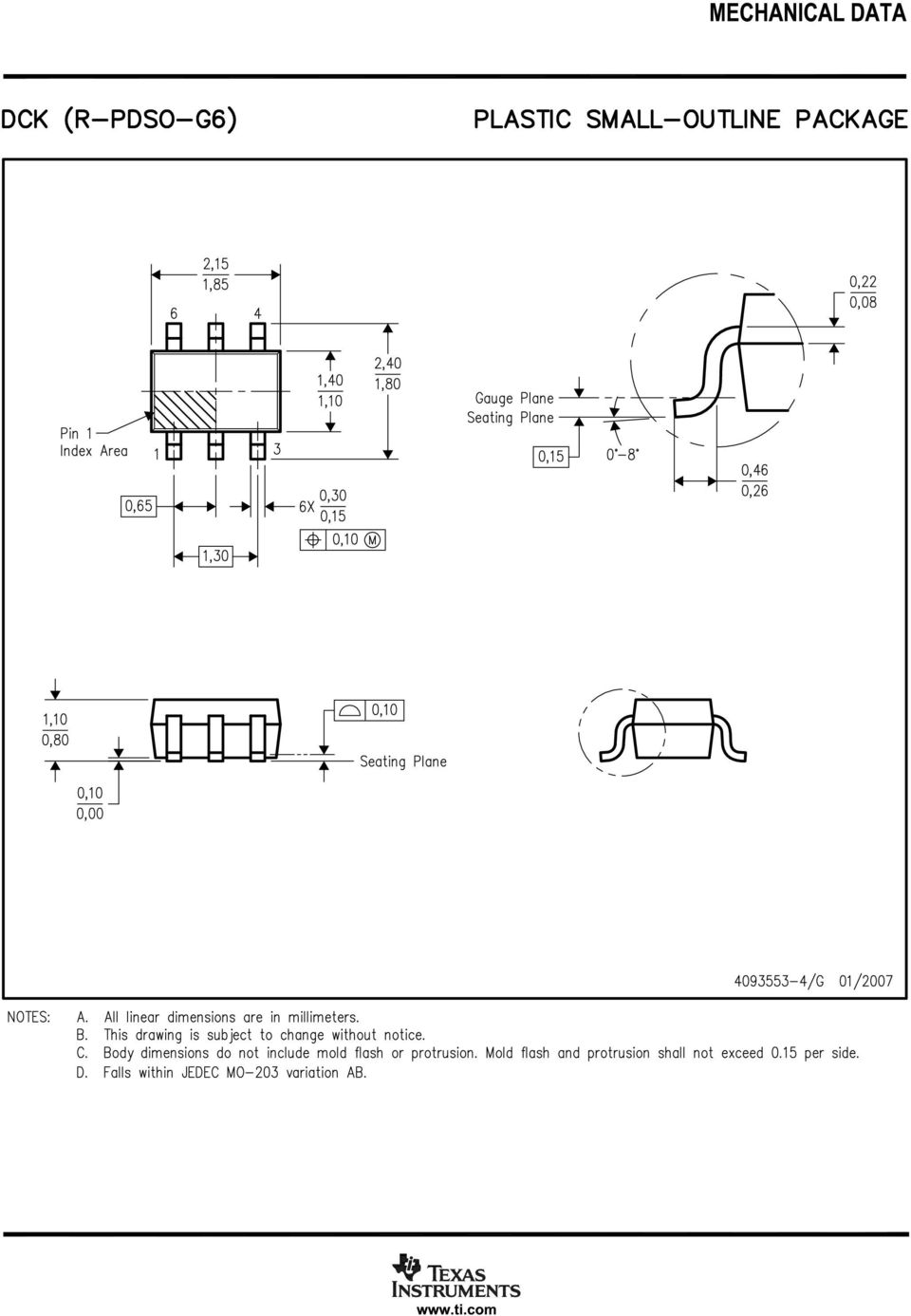
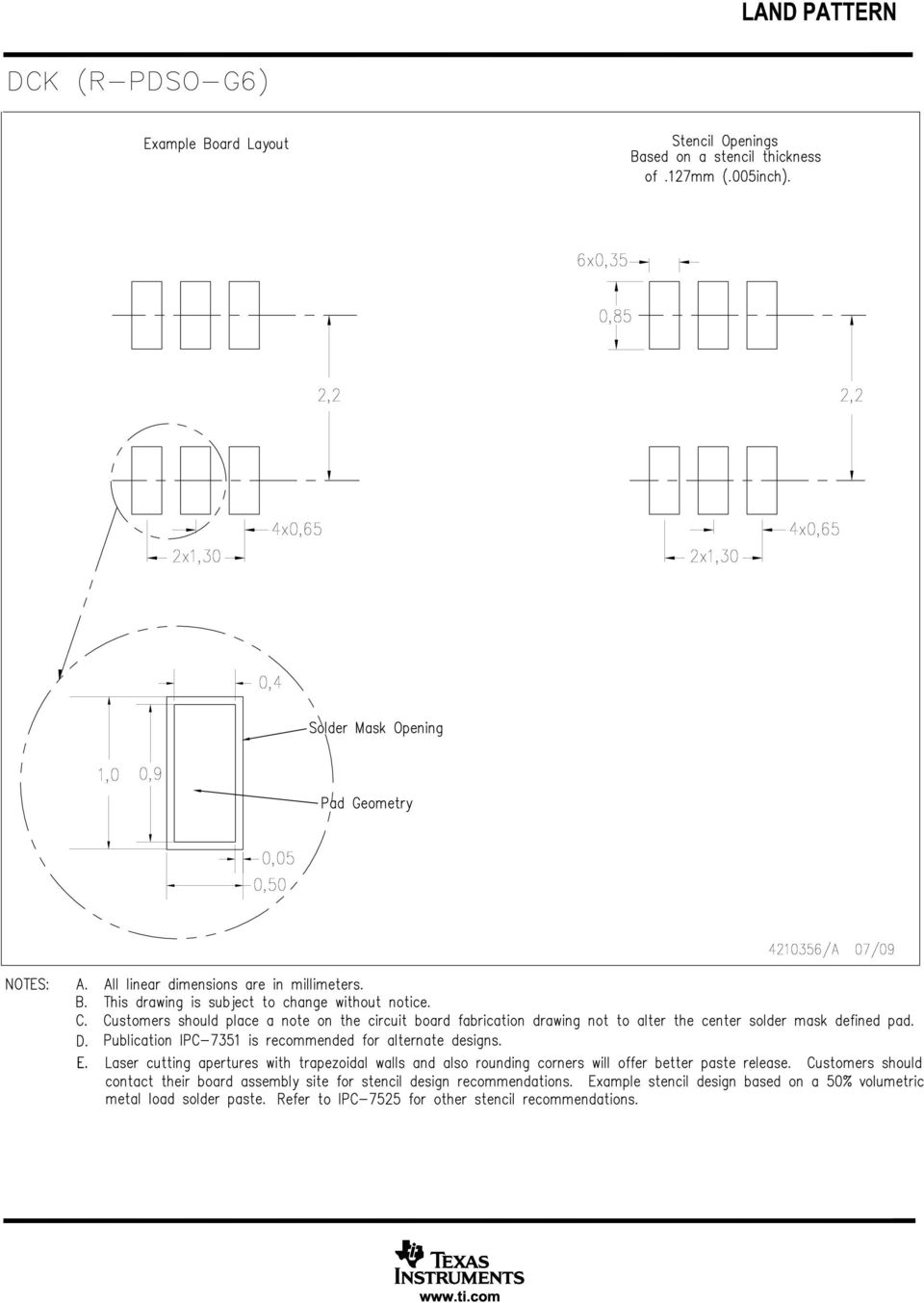
2 SB0S294E DECEMBER 2003 REVISED SEPTEMBER 2006 ORDERING INFORMATION (1) PRODUCT PACKAGE PACKAGE DESIGNATOR PACKAGE MARKING OPA360 SC70-6 DCK AUW (1) For the most current package and ordering information see the Package Option Addendum at at the end of this document, or see the TI web site at. ABSOLUTE MAXIMUM RATINGS (1) Supply Voltage, V+ to V V Signal Input Terminals, Voltage(2).... (V ) 0.5V to (V+) + 0.5V Current(2) ±10mA Output Short-Circuit through 75Ω to GND(3) Continuous Operating Temperature C to +85 C Storage Temperature C to +150 C Junction Temperature C (1) Stresses above these ratings may cause permanent damage. Exposure to absolute maximum conditions for extended periods may degrade device reliability. These are stress ratings only, and functional operation of the device at these or any other conditions beyond those specified is not implied. (2) Input terminals are diode-clamped to the power-supply rails. Input signals that can swing more than 0.5V beyond the supply rails should be current-limited to 10mA or less. (3) Short-circuit to ground. This integrated circuit can be damaged by ESD. Texas Instruments recommends that all integrated circuits be handled with appropriate precautions. Failure to observe proper handling and installation procedures can cause damage. ESD damage can range from subtle performance degradation to complete device failure. Precision integrated circuits may be more susceptible to damage because very small parametric changes could cause the device not to meet its published specifications. PIN CONFIGURATION OPA360 +In GND 1 2 LPF AUW 6 5 V+ Enable SAG 3 4 Out SC70 6 (1) (1) Pin 1 of the SC70-6 is determined by orienting the package marking as indicated in the diagram. 2
 Stresses above these ratings may cause permanent damage.")
3 SB0S294E DECEMBER 2003 REVISED SEPTEMBER 2006 ELECTRICAL CHARACTERISTICS: V S = +2.7V to +3.3V Single-Supply Boldface limits apply over the temperature range, T A = 40 C to +85 C. All specifications at T A = +25 C, R L = 150Ω connected to GND, unless otherwise noted. OFFSET LEVEL-SHIFT VOLTAGE OPA360 PARAMETER CONDITIONS MIN TYP MAX UNITS Output Level-Shift Voltage (1) V OLS V S = +3.3V, V IN = GND, G = mv Over Temperature Specified Temperature Range 60 mv vs. Power Supply PSRR V S = +2.7V to +3.3V ±80 µv/v INPUT BIAS CURRENT Input Bias Current I B ±3 pa INPUT VOLTAGE RANGE Common-Mode Voltage Range (2) V CM V S = 3.3V, G = +2 GND (V+) 1.5 V VOLTAGE GAIN V S = +3.3V, 0 < V IN < 1.5V db FREQUENCY RESPONSE Filter Response Normalized Gain: f IN = 4.5MHz V O = 2V PP db f IN = 27MHz V O = 2V PP db Differential Gain Error R L = 150Ω 0.5 % Differential Phase Error R L = 150Ω 1 Group Delay Variation 100kHz, 5MHz 13 ns Signal-to-Noise Ratio SNR 100% White Signal 70 db OUTPUT Positive Voltage Output Swing from Rail V S = +3.3V, G = 2, V IN = 2V, R L = 150Ω to GND mv Negative Voltage Output Swing from Rail V S = +3.3V, G = 2, V IN = 0V, R L = 150Ω to GND 3 25 mv Positive Voltage Output Swing from Rail V S = +3.3V, G = 2, V IN = 2V, R L = 75Ω to GND 300 mv Negative Voltage Output Swing from Rail V S = +3.3V, G = 2, V IN = 0V, R L = 75Ω to GND 10 mv Output Current (3) I O V S = +3.3V ±80 ma POWER SUPPLY Specified Voltage Range V S V Minimum Operating Voltage Range 2.5 to 3.6 V Quiescent Current I Q V S = +3.3V, Enabled, I O = ma ENABLE/SHUTDOWN FUNCTION Specified Temperature Range 9 ma Disabled (logic-low Threshold) 0.8 V Enabled (logic-high Threshold) 1.6 V Enable Time 1.5 µs Disable Time 50 ns Shutdown Current V S = +3.3, Disabled µa TEMPERATURE RANGE Specified Range C Operating Range C Storage Range C Thermal Resistance JA SC C/W (1) Output referred. Tested with SAG pin connected to OUT pin. (2) Limited by output swing and internal G = 2. Tested with the SAG pin connected to OUT pin. (3) See typical characteristics Output Voltage Swing vs Output Current. 3

4 SB0S294E DECEMBER 2003 REVISED SEPTEMBER 2006 TYPICAL CHARACTERISTICS: V S = 3.3V At TA = +25 C and RL = 150Ω, unless otherwise noted. Normalized Gain (db) FREQUENCY RESPONSE Population Normalized Gain at 4.5MHz Production Distribution Normalized: 0 db corresponds to 6dB gain k 100k 1M 10M 100M Frequency (Hz) Normalized Gain at 4.5MHz (db) Group Delay (ns) GROUP DELAY vs FREQUENCY k 100k 1M 10M Frequency (Hz) Gain Error (%) GAIN ERROR Temperature (C) Output Voltage (V) OUTPUT VOLTAGE SWING TO THE POSITIVE RAIL vs OUTPUT CURRENT Output Current (A) 40C V S =3.3V +85C +25C Output Voltage (V) OUTPUTVOLTAGESWINGTOTHENEGATIVERAIL vs OUTPUT CURRENT V S =3.3V,V IN =0V +85C Output Current (A) 40C +25C 4
 Group Delay (ns) GROUP DELAY vs FREQUENCY 45 40 35 30 25 20 15 10 5 0 10k 100k 1M 10M Frequency (Hz) Gain Error (%) GAIN ERROR 2.0 1.8 1.6 1.4 1.2 1.0 0.8 0.6 0.4 0.")
5 SB0S294E DECEMBER 2003 REVISED SEPTEMBER 2006 TYPICAL CHARACTERISTICS: V S = 3.3V (continued) At TA = +25 C and RL = 150Ω, unless otherwise noted. 7 6 QUIESCENT CURRENT vs SUPPLY VOLTAGE QUIESCENT CURRENT vs TEMPERATURE V S =3.3V Quiescent Current (ma) Quiescent Current (ma) Supply Voltage (V) Temperature (C) DIFFERENTIAL GAIN 3.0 SHUTDOWN CURRENT vs TEMPERATURE DIFFERENTIAL PHASE Shutdown Current (µa) V S =3.3V Temperature (C) SHUTDOWN TRIGGER LEVELS LARGE SIGNAL DISABLE/ENABLE RESPONSE Quiescent Current (ma) OPA360 Shutdown OPA360 Active Voltage (500mV/div) Enable OPA360 Output Disable Enable Pin Voltage (V) Time (1µs/div) 5
 SHUTDOWN TRIGGER LEVELS LARGE SIGNAL DISABLE/ENABLE RESPONSE Quiescent Current (ma) 6 4 2 OPA360 Shutdown OPA360 Active Voltage (500mV/div) Enable OPA360")
6 SB0S294E DECEMBER 2003 REVISED SEPTEMBER 2006 APPLICATIONS INFORMATION The OPA360 video amplifier has been optimized for portable video applications: Internal gain setting resistors (G = 2) reduce the number of external components needed in the video circuit. A 2-pole filter is incorporated for DAC signal reconstruction. The sag correction function reduces the size of the output coupling capacitors without compromising performance. OPA360 employs an internal level shift circuit that avoids sync pulse clipping and allows DC-coupled output. A shutdown feature reduces quiescent current to less than 5µA crucial for portable applications such as digital still cameras (DSCs) and camera phones. The OPA360 interfaces to digital media processors (DM320/270, DSC25). It has been optimized for the requirements of digital still cameras and cell phone/camera designs. OPERATING VOLTAGE The OPA360 is fully specified from 2.7V to 3.3V over a temperature range of 40 C to +85 C. Parameters that vary significantly with operating voltages or temperature are shown in the Typical Characteristics. Power-supply pins should be bypassed with 100nF ceramic capacitors. INPUT VOLTAGE The input common-mode range of the OPA360 series extends from GND to (V+) 1.5V. Because of the internal gain, the input voltage range necessary for an output in the valid range will be limited. INPUT OVERVOLTAGE PROTECTION All OPA360 pins are static-protected with internal ESD protection diodes connected to the supplies. These diodes will provide input overdrive protection if the current is externally limited to 10mA ENABLE/SHUTDOWN The OPA360 has a shutdown feature that disables the output and reduces the quiescent current to less than 5µA. This feature is especially useful for portable video applications such as digital still cameras and camera phones, where the equipment is infrequently connected to a TV or other video device. The Enable logic input voltage is referenced to the OPA360 GND pin. A logic level HIGH applied to the enable pin enables the op amp. A valid logic HIGH is defined as 1.6V above GND. A valid logic LOW is defined as 0.8V above GND. If the Enable pin is not connected, internal pull-up circuitry will enable the amplifier. Enable pin voltage levels are tested for a valid logic HIGH threshold of 1.6V minimum and a valid logic LOW threshold of 0.8V maximum. INTERNAL 2-POLE FILTER The OPA360 filter is a Sallen-Key topology with a 9MHz cutoff frequency. This allows the video signals to pass without any visible distortion, as shown in Figure 3 through Figure 5. The video DACs embedded in TI s Digital Media Processors over-sample at 27MHz. At this frequency, the attenuation is typically 21dB, which effectively attenuates the sampling aliases. The filter characteristics vary somewhat with signal source impedance. A source impedance greater than 500Ω can degrade filter performance. With current-output video DACs, a resistor to GND is often used to create a voltage output which is then applied to the OPA360 input (see Figure 1). TI s Digital Media Processors, such as the DM270 or DM320, typically use a 200Ω resistor to GND to convert the current output signal. This 200Ω source impedance does not degrade video performance. 10pF ( ) 1.1kΩ 1.4kΩ V O 75Ω Television R (1) 12pF 845Ω 75Ω 325Ω 528Ω SAG NOTE: (1) Optional. 650Ω OPA360 Figure 1. Filter Structure of OPA360 6

7 A capacitor placed in parallel with the resistor (Figure 1) creates an additional filter pole that provides additional stop-band attenuation. With a 200Ω source impedance, a 67pF ceramic capacitor provides approximately 28dB attenuation at 27MHz without affecting the pass band. VIDEO PERFORMANCE Industry standard video test patterns include: Multiburst packets of different test frequencies to check for basic frequency response. Multipulse pulses modulated at different frequencies to test for comprehensive measurement SB0S294E DECEMBER 2003 REVISED SEPTEMBER 2006 of amplitude and group delay errors across the video baseband. Chrominance-to-luminence (CCIR17) tests amplitude, phase and some distortion 50Hz, 1/2 black 1/2 white screen test signal tests the worst case signal swing required by the amplifier. Performance on these test signals are shown. Figure 2 shows the test circuits for Figure 3 through Figure 13 and Figure 16. (NOTE: 1 and 2 indicate measurement points corresponding to the waveforms labeled 1 and 2 in the figures.) µF µF SAG a. Test circuit for Figures 3 5. b. Test circuit for Figures 6, 8, and µF 1 C OUT µF 22µF c. Test circuits for Figures 10 and 11. d. Test circuit for Figures 7, 12, and 13. NOTE: 1 and 2 indicate measurement points corresponding to the waveforms labeled 1 and 2 in the figures. Figure 2. Test Circuits Used for Figures

8 SB0S294E DECEMBER 2003 REVISED SEPTEMBER 2006 FREQUENCY RESPONSE OF THE OPA360 Frequency response measurements evaluate the ability of a video system to uniformly transfer signal components of different frequencies without affecting their respective amplitudes. Figure 3 shows the multiburst test pattern; Figure 4 shows the multipulse. The top waveforms in these figures show the full test pattern. The middle and bottom waveform are a more detailed view of the critical portion of the full waveform. The middle waveform represents the input signal from the video generator; the bottom waveform is the OPA360 output to the line. Chrominance-to-luminence gain inequality (or relative chrominance level) is a change in the gain ratio of the chrominance and luminence components of a video signal, which are at different frequencies. A common test pattern is the pulse in test pattern CCIR 17, shown in Figure 5. As in Figure 3 and Figure 4, the top waveform shows the full test pattern; the middle and bottom waveform are a more detailed view of the critical portion of the full waveform, with the middle waveform representing the input signal from the video generator and the bottom waveform being the OPA360 output to the line. Figure 3. Multiburst (CCIR 18) Test Pattern (PAL) Figure 5. CCIR 17 Test Pattern (PAL) Gain errors most commonly appear as attenuation or peaking of the chrominance information. This shows up in the picture as incorrect color saturation. Delay distortion will cause color smearing or bleeding, particularly at the edges of objects in the picture. It may also cause poor reproduction of sharp luminence transitions. All waveforms in Figure 3 through Figure 5 were taken using the sag correction feature of OPA360. Figure 3 through Figure 5 show that the OPA360 causes no visible distortion or change in gain throughout the entire video frequency range. Figure 4. Multipulse Test Pattern (PAL) INTERNAL LEVEL SHIFT Many common video DACs embedded in digital media processors like TI s TMS320DM270 and the new OMAP2420 processors operate on a single supply (no negative supply). Typically, the lowest point of the sync pulse output by these Video DACs corresponds to 0V. With a 0V input, the output of common single-supply op amps saturates at a voltage > 0V. This effect would clip the tip of the sync pulse and therefore degrade the video signal integrity. The OPA360 employs an internal level shift circuit to avoid clipping. The input signal is typically shifted by 8

9 SB0S294E DECEMBER 2003 REVISED SEPTEMBER 2006 approximately 60mV. This is well within the linear output voltage range of the OPA360 with a standard 150Ω video load. Figure 6 shows the function of the level shifter. Figure 7. Output Swing with 33F on 3V Supply Figure 6. Internal Level Shifter, Shifts Input Signal by Approximately 60mV to Prevent Sync Tip Clipping OUTPUT SWING TO GND (SYNC PULSE) Figure 8 shows the true output swing capability of the OPA360 by taking the tip of the input sync pulse to a slightly negative voltage. Even when the output sync tip is at 8mV, the output shows no clipping of the sync pulse. The level shift function is particularly useful when the output of the OPA360 is DC-coupled to the video load. However, it is also helpful when sag correction is employed. The offset helps to shift the video signal closer to the positive rail, so that with even a small 33µF coupling capacitor, the output is well outside the saturation limits of the OPA360. Figure 7 shows the output swing of the OPA360, operated on 3.0V supplies, with a 22µF sag correction capacitor and a 33µF output coupling capacitor. The test signal is a 50Hz signal constructed to generate a 1/2 black, 1/2 white screen. This video pattern is one of the most difficult patterns to display because it is the worst case signal regarding signal swing. A worst case signal such as this is highly unlikely in normal operation. Any other signal has a lower swing range. Note in Figure 7 that neither the white nor the black portion of the video signal is clipped. Figure 8. Input Sync Tip at 30mV (Output Shows No Sign of Clipping) 9

10 SB0S294E DECEMBER 2003 REVISED SEPTEMBER 2006 SAG CORRECTION Sag correction provides excellent video performance with two small output coupling capacitors. It eliminates the traditional, large 220µF output capacitor. The traditional 220µF circuit (Figure 9a) creates a single low frequency pole ( 3dB frequency) at 5Hz. If this capacitor is made much smaller, excessive phase shift in the critical 50 to 100Hz range produces field tilt which can interfere with proper recovery of synchronization signals in the television receiver. The OPA360 sag correction circuit (Figure 9b, see also Figure 14) creates an amplitude response peak in the 20Hz region. This small amount of peaking (a few tenths of a db) provides compensation of the phase response in the critical 50Hz to 100Hz range, greatly reducing field tilt. Note that two significantly smaller and lower cost capacitors are required. 220µF 75Ω 75Ω Figure 10. Standard Video Circuit with 220F Capacitor (top trace) vs OPA360 with 22F and 47F Capacitors a) Traditional Video Circuit 47µF 75Ω A field tilt equivalent to that achieved using the standard 220µF coupling capacitor can be achieved with a 22µF/67µF combination see Figure 11. These capacitor values are optimized sag correction capacitors larger than 22µF do not provide significant improvement. Smaller sag correction capacitors will lead to higher tilt. 22µF 75Ω b) OPA360 with Sag Correction Figure 9. Traditional Video Circuit vs OPA360 with Sag Correction To achieve good performance, a 22µF sag correction and 47µF coupling capacitor can be used. Figure 10 and Figure 11 show comparisons for a standard video circuit with a 220µF coupling capacitor and the OPA360 with sag correction. Figure 10 shows that the 22µF/47µF combination leads to only a slightly greater tilt in the 50Hz, 1/2 black 1/2 white video signal. No degradation in video quality is observed. Figure F Standard Video Circuit (top trace) vs OPA360 with 22F and 67F Capacitors 10
 creates an amplitude response peak in the 20Hz region.")
11 SUPPLY VOLTAGE vs COUPLING CAPACITOR The output voltage swing is a function of the coupling capacitor value. The value of the sag correction capacitor has only a minor influence. The smaller the coupling capacitor, the greater the output swing. Therefore, to accommodate the large signal swing with very small coupling capacitors (22µF and 33µF), a higher supply voltage might be needed. SB0S294E DECEMBER 2003 REVISED SEPTEMBER 2006 As seen in Figure 7, the output swing with a 33µF coupling capacitor is already very close to the saturation limit on a 3V supply. Over time and temperature, a capacitor might change its value slightly, which in turn could force the output into saturation. Using the 50Hz, 1/2 black1/2 white screen test signal as a worst-case analysis, Figure 12 and Figure 13 demonstrate that a 3V supply could be used with a coupling capacitor as low as 47µF. Figure 12. Output Swing with 47F on 3V Supply Figure 13. Output Swing with 67F on 3V Supply V+ = 2.7V to 3.3V ENABLE V+ Video DAC (1) OPA360 2 Pole Filter Level Shifter Enable OUT C OUT 47µF + R OUT 75Ω C SAG 22µF + 75Ω GND SAG AC Gain = 2 DC Gain = 2.8 Television or VCR NOTE: (1) Optional 200Ωfor use with TI s Digital Media Processors. Figure 14. DC-Coupled Input/AC-Coupled Output 11

12 SB0S294E DECEMBER 2003 REVISED SEPTEMBER 2006 DC-COUPLED OUTPUT Due to the internal level shift, the OPA360 can also be DCcoupled to a video load. As shown in Figure 15, this eliminates the need for AC-coupling capacitors at the output. This is especially important in portable video applications where board space is restricted. The DC-coupled output configuration also shows the best video performance. As seen in Figure 16, there is no line or field tilt allowing use of the lowest power supply. In this mode, the OPA360 will safely operate down to 2.5V with no clipping of the signal. The disadvantage with DC-coupled output is that it uses somewhat higher supply current. V+=2.7Vto3.3V ENABLE V+ Video DAC (1) OPA360 2 Pole Filter Level Shifter Enable OUT R OUT 75Ω 6dB 75Ω GND SAG Television or VCR NOTE: (1) Optional 200Ωfor use with TI s Digital Media Processors. Figure 15. DC-Coupled Input/DC-Coupled Output Figure 16. DC-Coupled Output 12

13 PACKAGE OPTION ADDENDUM 12-Sep-2006 PACKAGING INFORMATION Orderable Device Status (1) Package Type Package Drawing Pins Package Qty OPA360AIDCKR ACTIVE SC70 DCK Green (RoHS & no Sb/Br) OPA360AIDCKRE4 ACTIVE SC70 DCK Green (RoHS & no Sb/Br) OPA360AIDCKT ACTIVE SC70 DCK Green (RoHS & no Sb/Br) OPA360AIDCKTG4 ACTIVE SC70 DCK Green (RoHS & no Sb/Br) Eco Plan (2) Lead/Ball Finish MSL Peak Temp (3) CU NIPDAU CU NIPDAU CU NIPDAU CU NIPDAU Level-2-260C-1 YEAR Level-2-260C-1 YEAR Level-2-260C-1 YEAR Level-2-260C-1 YEAR (1) The marketing status values are defined as follows: ACTIVE: Product device recommended for new designs. LIFEBUY: TI has announced that the device will be discontinued, and a lifetime-buy period is in effect. NRND: Not recommended for new designs. Device is in production to support existing customers, but TI does not recommend using this part in a new design. PREVIEW: Device has been announced but is not in production. Samples may or may not be available. OBSOLETE: TI has discontinued the production of the device. (2) Eco Plan - The planned eco-friendly classification: Pb-Free (RoHS), Pb-Free (RoHS Exempt), or Green (RoHS & no Sb/Br) - please check for the latest availability information and additional product content details. TBD: The Pb-Free/Green conversion plan has not been defined. Pb-Free (RoHS): TI's terms "Lead-Free" or "Pb-Free" mean semiconductor products that are compatible with the current RoHS requirements for all 6 substances, including the requirement that lead not exceed 0.1% by weight in homogeneous materials. Where designed to be soldered at high temperatures, TI Pb-Free products are suitable for use in specified lead-free processes. Pb-Free (RoHS Exempt): This component has a RoHS exemption for either 1) lead-based flip-chip solder bumps used between the die and package, or 2) lead-based die adhesive used between the die and leadframe. The component is otherwise considered Pb-Free (RoHS compatible) as defined above. Green (RoHS & no Sb/Br): TI defines "Green" to mean Pb-Free (RoHS compatible), and free of Bromine (Br) and Antimony (Sb) based flame retardants (Br or Sb do not exceed 0.1% by weight in homogeneous material) (3) MSL, Peak Temp. -- The Moisture Sensitivity Level rating according to the JEDEC industry standard classifications, and peak solder temperature. Important Information and Disclaimer:The information provided on this page represents TI's knowledge and belief as of the date that it is provided. TI bases its knowledge and belief on information provided by third parties, and makes no representation or warranty as to the accuracy of such information. Efforts are underway to better integrate information from third parties. TI has taken and continues to take reasonable steps to provide representative and accurate information but may not have conducted destructive testing or chemical analysis on incoming materials and chemicals. TI and TI suppliers consider certain information to be proprietary, and thus CAS numbers and other limited information may not be available for release. In no event shall TI's liability arising out of such information exceed the total purchase price of the TI part(s) at issue in this document sold by TI to Customer on an annual basis. Addendum-Page 1

14 PACKAGE MATERIALS INFORMATION 23-Jan-2009 TAPE AND REEL INFORMATION *All dimensions are nominal Device Package Type Package Drawing Pins SPQ Reel Reel Diameter Width (mm) W1 (mm) A0 (mm) B0 (mm) K0 (mm) P1 (mm) OPA360AIDCKR SC70 DCK Q3 OPA360AIDCKT SC70 DCK Q3 W (mm) Pin1 Quadrant Pack Materials-Page 1
 Pin1 Quadrant Pack Materials-Page 1")
15 PACKAGE MATERIALS INFORMATION 23-Jan-2009 *All dimensions are nominal Device Package Type Package Drawing Pins SPQ Length (mm) Width (mm) Height (mm) OPA360AIDCKR SC70 DCK OPA360AIDCKT SC70 DCK Pack Materials-Page 2

16
17
18 PACKAGE OPTION ADDENDUM 10-Jun-2014 PACKAGING INFORMATION Orderable Device Status (1) Package Type Package Drawing Pins Package Qty Eco Plan OPA360AIDCKR ACTIVE SC70 DCK Green (RoHS & no Sb/Br) OPA360AIDCKRG4 ACTIVE SC70 DCK Green (RoHS & no Sb/Br) OPA360AIDCKT ACTIVE SC70 DCK Green (RoHS & no Sb/Br) OPA360AIDCKTG4 ACTIVE SC70 DCK Green (RoHS & no Sb/Br) (2) Lead/Ball Finish (6) MSL Peak Temp (3) Op Temp ( C) Device Marking (4/5) CU NIPDAU Level-2-260C-1 YEAR -40 to 85 AUW CU NIPDAU Level-2-260C-1 YEAR -40 to 85 AUW CU NIPDAU Level-2-260C-1 YEAR -40 to 85 AUW CU NIPDAU Level-2-260C-1 YEAR -40 to 85 AUW Samples (1) The marketing status values are defined as follows: ACTIVE: Product device recommended for new designs. LIFEBUY: TI has announced that the device will be discontinued, and a lifetime-buy period is in effect. NRND: Not recommended for new designs. Device is in production to support existing customers, but TI does not recommend using this part in a new design. PREVIEW: Device has been announced but is not in production. Samples may or may not be available. OBSOLETE: TI has discontinued the production of the device. (2) Eco Plan - The planned eco-friendly classification: Pb-Free (RoHS), Pb-Free (RoHS Exempt), or Green (RoHS & no Sb/Br) - please check for the latest availability information and additional product content details. TBD: The Pb-Free/Green conversion plan has not been defined. Pb-Free (RoHS): TI's terms "Lead-Free" or "Pb-Free" mean semiconductor products that are compatible with the current RoHS requirements for all 6 substances, including the requirement that lead not exceed 0.1% by weight in homogeneous materials. Where designed to be soldered at high temperatures, TI Pb-Free products are suitable for use in specified lead-free processes. Pb-Free (RoHS Exempt): This component has a RoHS exemption for either 1) lead-based flip-chip solder bumps used between the die and package, or 2) lead-based die adhesive used between the die and leadframe. The component is otherwise considered Pb-Free (RoHS compatible) as defined above. Green (RoHS & no Sb/Br): TI defines "Green" to mean Pb-Free (RoHS compatible), and free of Bromine (Br) and Antimony (Sb) based flame retardants (Br or Sb do not exceed 0.1% by weight in homogeneous material) (3) MSL, Peak Temp. - The Moisture Sensitivity Level rating according to the JEDEC industry standard classifications, and peak solder temperature. (4) There may be additional marking, which relates to the logo, the lot trace code information, or the environmental category on the device. (5) Multiple Device Markings will be inside parentheses. Only one Device Marking contained in parentheses and separated by a "~" will appear on a device. If a line is indented then it is a continuation of the previous line and the two combined represent the entire Device Marking for that device. (6) Lead/Ball Finish - Orderable Devices may have multiple material finish options. Finish options are separated by a vertical ruled line. Lead/Ball Finish values may wrap to two lines if the finish value exceeds the maximum column width. Addendum-Page 1
 The marketing status values are defined as follows: ACTIVE: Product device recommended for new designs.")
19 PACKAGE OPTION ADDENDUM 10-Jun-2014 Important Information and Disclaimer:The information provided on this page represents TI's knowledge and belief as of the date that it is provided. TI bases its knowledge and belief on information provided by third parties, and makes no representation or warranty as to the accuracy of such information. Efforts are underway to better integrate information from third parties. TI has taken and continues to take reasonable steps to provide representative and accurate information but may not have conducted destructive testing or chemical analysis on incoming materials and chemicals. TI and TI suppliers consider certain information to be proprietary, and thus CAS numbers and other limited information may not be available for release. In no event shall TI's liability arising out of such information exceed the total purchase price of the TI part(s) at issue in this document sold by TI to Customer on an annual basis. Addendum-Page 2

20 PACKAGE MATERIALS INFORMATION 11-Jul-2013 TAPE AND REEL INFORMATION *All dimensions are nominal Device Package Type Package Drawing Pins SPQ Reel Diameter (mm) Reel Width W1 (mm) A0 (mm) B0 (mm) K0 (mm) P1 (mm) W (mm) Pin1 Quadrant OPA360AIDCKR SC70 DCK Q3 OPA360AIDCKR SC70 DCK Q3 OPA360AIDCKT SC70 DCK Q3 OPA360AIDCKT SC70 DCK Q3 Pack Materials-Page 1

21 PACKAGE MATERIALS INFORMATION 11-Jul-2013 *All dimensions are nominal Device Package Type Package Drawing Pins SPQ Length (mm) Width (mm) Height (mm) OPA360AIDCKR SC70 DCK OPA360AIDCKR SC70 DCK OPA360AIDCKT SC70 DCK OPA360AIDCKT SC70 DCK Pack Materials-Page 2
22
23
24 IMPORTANT NOTICE Texas Instruments Incorporated and its subsidiaries (TI) reserve the right to make corrections, enhancements, improvements and other changes to its semiconductor products and services per JESD46, latest issue, and to discontinue any product or service per JESD48, latest issue. Buyers should obtain the latest relevant information before placing orders and should verify that such information is current and complete. All semiconductor products (also referred to herein as components ) are sold subject to TI s terms and conditions of sale supplied at the time of order acknowledgment. TI warrants performance of its components to the specifications applicable at the time of sale, in accordance with the warranty in TI s terms and conditions of sale of semiconductor products. Testing and other quality control techniques are used to the extent TI deems necessary to support this warranty. Except where mandated by applicable law, testing of all parameters of each component is not necessarily performed. TI assumes no liability for applications assistance or the design of Buyers products. Buyers are responsible for their products and applications using TI components. To minimize the risks associated with Buyers products and applications, Buyers should provide adequate design and operating safeguards. TI does not warrant or represent that any license, either express or implied, is granted under any patent right, copyright, mask work right, or other intellectual property right relating to any combination, machine, or process in which TI components or services are used. Information published by TI regarding third-party products or services does not constitute a license to use such products or services or a warranty or endorsement thereof. Use of such information may require a license from a third party under the patents or other intellectual property of the third party, or a license from TI under the patents or other intellectual property of TI. Reproduction of significant portions of TI information in TI data books or data sheets is permissible only if reproduction is without alteration and is accompanied by all associated warranties, conditions, limitations, and notices. TI is not responsible or liable for such altered documentation. Information of third parties may be subject to additional restrictions. Resale of TI components or services with statements different from or beyond the parameters stated by TI for that component or service voids all express and any implied warranties for the associated TI component or service and is an unfair and deceptive business practice. TI is not responsible or liable for any such statements. Buyer acknowledges and agrees that it is solely responsible for compliance with all legal, regulatory and safety-related requirements concerning its products, and any use of TI components in its applications, notwithstanding any applications-related information or support that may be provided by TI. Buyer represents and agrees that it has all the necessary expertise to create and implement safeguards which anticipate dangerous consequences of failures, monitor failures and their consequences, lessen the likelihood of failures that might cause harm and take appropriate remedial actions. Buyer will fully indemnify TI and its representatives against any damages arising out of the use of any TI components in safety-critical applications. In some cases, TI components may be promoted specifically to facilitate safety-related applications. With such components, TI s goal is to help enable customers to design and create their own end-product solutions that meet applicable functional safety standards and requirements. Nonetheless, such components are subject to these terms. No TI components are authorized for use in FDA Class III (or similar life-critical medical equipment) unless authorized officers of the parties have executed a special agreement specifically governing such use. Only those TI components which TI has specifically designated as military grade or enhanced plastic are designed and intended for use in military/aerospace applications or environments. Buyer acknowledges and agrees that any military or aerospace use of TI components which have not been so designated is solely at the Buyer's risk, and that Buyer is solely responsible for compliance with all legal and regulatory requirements in connection with such use. TI has specifically designated certain components as meeting ISO/TS16949 requirements, mainly for automotive use. In any case of use of non-designated products, TI will not be responsible for any failure to meet ISO/TS Products Applications Audio /audio Automotive and Transportation /automotive Amplifiers amplifier.ti.com Communications and Telecom /communications Data Converters dataconverter.ti.com Computers and Peripherals /computers DLP Products Consumer Electronics /consumer-apps DSP dsp.ti.com Energy and Lighting /energy Clocks and Timers /clocks Industrial /industrial Interface interface.ti.com Medical /medical Logic logic.ti.com Security /security Power Mgmt power.ti.com Space, Avionics and Defense /space-avionics-defense Microcontrollers microcontroller.ti.com Video and Imaging /video RFID OMAP Applications Processors /omap TI E2E Community e2e.ti.com Wireless Connectivity /wirelessconnectivity Mailing Address: Texas Instruments, Post Office Box , Dallas, Texas Copyright 2014, Texas Instruments Incorporated
Data sheet acquired from Harris Semiconductor SCHS078C -- Revised October 2003
 Data sheet acquired from Harris Semiconductor SCHS078C -- Revised October 2003 The CD4521B types are supplied in 16-lead dual-in-line plastic packages (E suffix), 16-lead small-outline packages (M, M96,
SDLS940A MARCH 1974 REVISED MARCH 1988. Copyright 1988, Texas Instruments Incorporated
 SN5490A, SN5492A, SN5493A, SN54LS90, SN54LS92, SN54LS93 SN7490A, SN7492A, SN7493A, SN74LS90, SN74LS92, SN74LS93 DECADE, DIVIDE-BY-TWELVE AND BINARY COUNTERS SDLS940A MARCH 1974 REVISED MARCH 1988 PRODUCTION
with Ultra-Fast Transient Response and High Light-Load Efficiency
 1 Adaptor 6-24V Optional N-FET Driver Ultra-Fast DPM Simplified Application Diagram Iin Ultra-Low Quiescent Current Enhanced Safety Features OCP, OVP, FET Short Support CPU Turbo Mode To System bq24715
CD4071B Quad 2-Input OR Gate CD4072B Dual 4-Input OR Gate CD4075B Triple 3-Input OR Gate
 Data sheet acquired from Harris Semiconductor SCHS056D Revised August 2003 CD4071B Quad 2-Input OR Gate CD4072B Dual 4-Input OR Gate CD4075B Triple 3-Input OR Gate CD4071B, CD4072B, and CD4075B OR gates
Data sheet acquired from Harris Semiconductor SCHS049C Revised October 2003
 Data sheet acquired from Harris Semiconductor SCHS049C Revised October 2003 CD4060B consists of an oscillator section and 14 ripple-carry binary counter stages. The oscillator configuration allows design
Data sheet acquired from Harris Semiconductor SCHS020C Revised October 2003
 Data sheet acquired from Harris Semiconductor SCHS020C Revised October 2003 The CD4009UB and CD4010B types are supplied in 16-lead hermetic dual-in-line ceramic packages (F3A suffix), 16-lead dual-in-line
 PACKAGE OPTION ADDENDUM www.ti.com 12-Jan-2006 PACKAGING INFORMATION Orderable Device Status (1) Package Type Package Drawing Pins Package Qty Eco Plan (2) Lead/Ball Finish MSL Peak Temp (3) 76005012A
Data sheet acquired from Harris Semiconductor SCHS067B Revised July 2003
 Data sheet acquired from Harris Semiconductor SCHS067B Revised July 2003 The CD4502B types are supplied in 16-lead hermetic dual-in-line ceramic packages (F3A suffix), 16-lead dual-in-line plastic packages
AMC1100: Replacement of Input Main Sensing Transformer in Inverters with Isolated Amplifier
 Application Report SLAA552 August 2012 AMC1100: Replacement of Input Main Sensing Transformer in Inverters with Isolated Amplifier Ambreesh Tripathi and Harmeet Singh Analog/Digital Converters ABSTRACT
Data sheet acquired from Harris Semiconductor SCHS087D Revised October 2003
 Data sheet acquired from Harris Semiconductor SCHS087D Revised October 2003 The CD4555B and CD4556B types are supplied in 16-lead hermetic dual-in-line ceramic packages (F3A suffix), 16-lead dual-in-line
FEATURES APPLICATIONS
 FEATURES DIGITALLY-CONTROLLED ANALOG VOLUME CONTROL: Four Independent Audio Channels Serial Control Interface Zero Crossing Detection Mute Function WIDE GAIN AND ATTENUATION RANGE: +31.5dB to 95.5dB with
LM556 LM556 Dual Timer
 LM556 LM556 Dual Timer Literature Number: SNAS549 LM556 Dual Timer General Description The LM556 Dual timing circuit is a highly stable controller capable of producing accurate time delays or oscillation.
 PACKAGE OPTION ADDENDUM www.ti.com 12-Jan-2006 PACKAGING INFORMATION Orderable Device Status (1) Package Type Package Drawing Pins Package Qty Eco Plan (2) Lead/Ball Finish MSL Peak Temp (3) 5962-9557401QCA
LM5030 LM5030 Application: DC - DC Converter Utilizing the Push-Pull Topology
 LM5030 LM5030 Application: DC - DC Converter Utilizing the Push-Pull Topology Literature Number: SNVA553 LM5030 Application DC DC Converter Utilizing the Push-Pull Topology 1 Push-Pull Topology D1 L +
RF37S114 Tag-it HF-I Type 5 NFC, ISO/IEC 15693 Transponder, 4 mm 4 mm
 1 1 Product Folder Sample & Buy Technical Documents Tools & Software Support & Community RF37S114 SCBS907 NOVEMBER 2015 RF37S114 Tag-it HF-I Type 5 NFC, ISO/IEC 15693 Transponder, 4 mm 4 mm 1 Device Overview
Application Note AN107
 Murata Balun for CC253x and CC254x LFB182G45BG2D280 By Fredrik Kervel Keywords Balun LFB182G45BG2D280 CC253x CC254x CC257x CC85xx 1 Introduction Murata s LFB182G45BG2D280 integrated balun is specially
AUDIO DIFFERENTIAL LINE RECEIVER. 0dB (G = 1)
") INA4 INA4 INA4 INA4 INA4 INA4 AUDIO DIFFERENTIAL LINE RECEIVERS db (G = ) FEATURES SINGLE AND DUAL VERSIONS LOW DISTORTION:.% at f = khz HIGH SLEW RATE: 4V/µs FAST SETTLING TIME: µs to.% WIDE SUPPLY RANGE:
INA4 INA4 INA4 INA4 INA4 INA4 AUDIO DIFFERENTIAL LINE RECEIVERS db (G = ) FEATURES SINGLE AND DUAL VERSIONS LOW DISTORTION:.% at f = khz HIGH SLEW RATE: 4V/µs FAST SETTLING TIME: µs to.% WIDE SUPPLY RANGE:
Stereo Audio Volume Control
 PGA2320 Stereo Audio Volume Control FEATURES DIGITALLY-CONTROLLED ANALOG VOLUME CONTROL: Two Independent Audio Channels Serial Control Interface Zero Crossing Detection Mute Function WIDE GAIN AND ATTENUATION
LM709 LM709 Operational Amplifier
 LM709 LM709 Operational Amplifier Literature Number: SNOS659A LM709 Operational Amplifier General Description The LM709 series is a monolithic operational amplifier intended for general-purpose applications
Multi-Transformer LED TV Power User Guide. Anderson Hsiao
 Multi-Transformer LED TV Power User Guide Anderson Hsiao Operation Range Input Range: 90Vac~264Vac 47Hz~63Hz Dimming Range: Reverse Signal 0V ~ 5V 100Hz ~200Hz 1%~100% Output Range :STBY-5V 20mA~1A 5V
Wireless Subwoofer TI Design Tests
 Wireless Subwoofer TI Design Tests This system design was tested for THD+N vs. frequency at 5 watts and 30 watts and THD+N vs. power at 00. Both the direct analog input and the wireless systems were tested.
ELECTROSTATIC DISCHARGE SENSITIVITY
 INA INA SBOSD DECEMBER REVISED JANUARY micropower, Single-Supply, CMOS Instrumentation Amplifier FEATURES LOW QUIESCENT CURRENT: µa/channel Shut Down: < µa HIGH GAIN ACCURACY: G =,.%, ppm/ C GAIN SET WITH
1OE 3B NC 3B V GND ORDERING INFORMATION. QFN RGY Tape and reel SN74CBT3125RGYR CU125. SOIC D Tape and reel SN74CBT3125DR
 SN74CBT3125 QUADRUPLE FET BUS SWITCH SCDS021I MAY 1995 REVISED SEPTEMBER 2002 Standard 125-Type Pinout (D, DB, DGV, and PW Packages) 5-Ω Switch Connection Between Two Ports TTL-Compatible Input Levels
description typical application
 Overvoltage Protection and Lockout for 12 V, 5 V, 3.3 V Undervoltage Protection and Lockout for 5 V and 3.3 V Fault Protection Output With Open-Drain Output Stage Open-Drain Power Good Output Signal for
Low-Power, Single-Supply, CMOS INSTRUMENTATION AMPLIFIERS
 INA INA INA INA Low-Power, Single-Supply, CMOS INSTRUMENTATION AMPLIFIERS SBOSC DECEMBER REVISED APRIL FEATURES DESIGNED FOR LOW COST HIGH GAIN ACCURACY: G =,.%, ppm/ C GAIN SET WITH EXT. RESISTORS FOR
PACKAGE OPTION ADDENDUM
 PACKAGE OPTION ADDENDUM www.ti.com 10-Jun-2014 PACKAGING INFORMATION Orderable Device Status (1) Package Type Package Drawing Pins Package Qty Eco Plan (2) Lead/Ball Finish (6) MSL Peak Temp (3) Op Temp
24-Bit, 40kHz ANALOG-TO-DIGITAL CONVERTER
 SEPTEMBER 2 REVISED JUNE 26 24-Bit, 4kHz ANALOG-TO-DIGITAL CONVERTER FEATURES 24 BITS NO MISSING CODES 19 BITS EFFECTIVE RESOLUTION UP TO 4kHz DATA RATE LOW NOISE: 2.5ppm DIFFERENTIAL INPUTS INL:.15% (max)
Texas Instruments. FB PS LLC Test Report HVPS SYSTEM AND APPLICATION TEAM REVA
 Texas Instruments FB PS LLC Test Report HVPS SYSTEM AND APPLICATION TEAM REVA 12/05/2014 1 General 1.1 PURPOSE Provide the detailed data for evaluating and verifying the FB-PS-LLC. The FB-PS-LLC is a Full
16-Bit, 10µs Sampling, CMOS ANALOG-to-DIGITAL CONVERTER
 JANUARY 1996 REVISED OCTOBER 2006 16-Bit, 10µs Sampling, CMOS ANALOG-to-DIGITAL CONVERTER FEATURES 100kHz min SAMPLING RATE STANDARD ±10V INPUT RANGE 86dB min SINAD WITH 20kHz INPUT ±3.0 LSB max INL DNL:
Features. Ordering Information. * Underbar marking may not be to scale. Part Identification
 MIC86 Teeny Ultra Low Power Op Amp General Description The MIC86 is a rail-to-rail output, input common-mode to ground, operational amplifier in Teeny SC7 packaging. The MIC86 provides 4kHz gain-bandwidth
24-Bit, 20kHz, Low-Power ANALOG-TO-DIGITAL CONVERTER
 ADS1251 ADS1251 MARCH 21 REVISED JUNE 29 24-Bit, 2kHz, Low-Power ANALOG-TO-DIGITAL CONVERTER FEATURES 24 BITS NO MISSING CODES 19 BITS EFFECTIVE RESOLUTION UP TO 2kHz DATA RATE LOW NOISE: 1.5ppm DIFFERENTIAL
µa7800 SERIES POSITIVE-VOLTAGE REGULATORS
 SLS056J MAY 976 REISED MAY 2003 3-Terminal Regulators Output Current up to.5 A Internal Thermal-Overload Protection High Power-Dissipation Capability Internal Short-Circuit Current Limiting Output Transistor
16-Bit DIGITAL-TO-ANALOG CONVERTER With Serial Data Interface
 SBAS0A JULY 997 REVISED NOVEMBER 00 -Bit DIGITAL-TO-ANALOG CONVERTER With Serial Data Interface FEATURES: SERIAL DIGITAL INTERFACE VOLTAGE OUTPUT: ±0V, ±V, 0 to +0V ± LSB INTEGRAL LINEARITY -BIT MONOTONIC
4-20mA Current-Loop Transmitter
 4-0mA Current-Loop Transmitter SBOS44C SEPTEMBER 005 REVISED MAY 01 FEATURES LOW QUIESCENT CURRENT: 10μA 5V REGULATOR FOR EXTERNAL CIRCUITS LOW SPAN ERROR: 0.05% LOW NONLINEARITY ERROR: 0.00% WIDE-LOOP
LM388 LM388 1.5W Audio Power Amplifier
 LM388 LM388 1.5W Audio Power Amplifier Literature Number: SNOSBT8A LM388 1 5W Audio Power Amplifier General Description The LM388 is an audio amplifier designed for use in medium power consumer applications
54LS174,54LS175,DM54LS174,DM54LS175, DM74LS174,DM74LS175
 54LS174,54LS175,DM54LS174,DM54LS175, DM74LS174,DM74LS175 54LS174 DM54LS174 DM74LS174 54LS175 DM54LS175 DM74LS175 Hex/Quad D Flip-Flops with Clear Literature Number: SNOS290A 54LS174 DM54LS174 DM74LS174
High-Voltage, High-Current OPERATIONAL AMPLIFIER
 High-Voltage, High-Current OPERATIONAL AMPLIFIER SBOS93E MARCH 1999 REVISED OCTOBER 2 FEATURES HIGH OUTPUT CURRENT: 8A Continuous 1A Peak WIDE POWER-SUPPLY RANGE: Single Supply: +8V to +6V Dual Supply:
SN54LVT574, SN74LVT574 3.3-V ABT OCTAL EDGE-TRIGGERED D-TYPE FLIP-FLOPS WITH 3-STATE OUTPUTS
 SN54LVT574, SN74LVT574 3.3-V ABT OCTAL EDGE-TRIGGERED D-TYPE FLIP-FLOPS WITH 3-STATE OUTPUTS SCBS139D MAY 1992 REVISED JULY 1995 State-of-the-Art Advanced BiCMOS Technology (ABT) Design for 3.3-V Operation
TS321 Low Power Single Operational Amplifier
 SOT-25 Pin Definition: 1. Input + 2. Ground 3. Input - 4. Output 5. Vcc General Description The TS321 brings performance and economy to low power systems. With high unity gain frequency and a guaranteed
LM138,LM338. LM138/LM338 5-Amp Adjustable Regulators. Literature Number: SNVS771A
 LM138,LM338 LM138/LM338 5-Amp Adjustable Regulators Literature Number: SNVS771A LM138/LM338 5-Amp Adjustable Regulators General Description The LM138 series of adjustable 3-terminal positive voltage regulators
1.0A LOW DROPOUT LINEAR REGULATOR
 1.0A LOW DROPOUT LINEAR REGULATOR Description Pin Assignments The is a low dropout three-terminal regulator with 1.0A output current ability, and the dropout voltage is specified at typical 1.1V at 1.0A
Providing Continuous Gate Drive Using a Charge Pump
 Application Report Philip Meyer and John Tucker... Power Management Products ABSTRACT Certain applications require that output voltage regulation be maintained when the input voltage is only slightly higher
Calculating Gain for Audio Amplifiers
 Application eport SLOA105A October 003 evised September 005 Calculating Gain for Audio Amplifiers Audio Power Amplifiers ABSTACT This application report explains the different types of audio power amplifier
Analysis of Power Supply Topologies for IGBT Gate Drivers in Industrial
 Application Report SLAA672 July 2015 Analysis of Power Supply Topologies for IGBT Gate Drivers in Industrial Sanjay Pithadia, N. Navaneeth Kumar ABSTRACT This application report explains different parameters
Wide Bandwidth, Fast Settling Difet OPERATIONAL AMPLIFIER
 Wide Bandwidth, Fast Settling Difet OPERATIONAL AMPLIFIER FEATURES HIGH GAIN-BANDWIDTH: 35MHz LOW INPUT NOISE: 1nV/ Hz HIGH SLEW RATE: V/µs FAST SETTLING: 24ns to.1% FET INPUT: I B = 5pA max HIGH OUTPUT
APPLICATION NOTE BUILDING A QAM MODULATOR USING A GC2011 DIGITAL FILTER CHIP
 SLWA022 APPLICATION NOTE BUILDING A QAM MODULATOR USING A GC2011 DIGITAL CHIP October 6, 1994 1.0 INTRODUCTION This report describes how one can use the GC2011 Digital Filter chip to build digital modulators
INSTRUMENTATION AMPLIFIER With Precision Voltage Reference
 INSTRUMENTATION AMPLIFIER With Precision Voltage Reference FEATURES LOW QUIESCENT CURRENT: 46µA PRECISION VOLTAGE REFERENCE: 1.24V, 2.V, V or 1V SLEEP MODE LOW OFFSET VOLTAGE: 2µV max LOW OFFSET DRIFT:
ORDERING INFORMATION. TOP-SIDE MARKING PDIP N Tube SN74LS07N SN74LS07N PACKAGE. SOIC D Tape and reel SN74LS07DR
 The SN54LS07 and SN74LS17 are obsolete and are no longer supplied. Convert TTL Voltage Levels to MOS Levels High Sink-Current Capability Input Clamping Diodes Simplify System Design Open-Collector Driver
V OUT. I o+ & I o- (typical) 2.3A & 3.3A. Package Type
 2.3A & 3.3A. Package Type") July 25 th, 2012 Automotive Grade AUIRS4427S DUAL LOW SIDE DRIVER Features Gate drive supply range from 6 V to 20 V CMOS Schmitt-triggered inputs 3.3V and 5V logic compatible Two independent gate drivers
July 25 th, 2012 Automotive Grade AUIRS4427S DUAL LOW SIDE DRIVER Features Gate drive supply range from 6 V to 20 V CMOS Schmitt-triggered inputs 3.3V and 5V logic compatible Two independent gate drivers
Application Report. 1 Description of the Problem. Jeff Falin... PMP Portable Power Applications ABSTRACT
 Application Report SLVA255 September 2006 Minimizing Ringing at the Switch Node of a Boost Converter Jeff Falin... PMP Portable Power Applications ABSTRACT This application report explains how to use proper
TS555. Low-power single CMOS timer. Description. Features. The TS555 is a single CMOS timer with very low consumption:
 Low-power single CMOS timer Description Datasheet - production data The TS555 is a single CMOS timer with very low consumption: Features SO8 (plastic micropackage) Pin connections (top view) (I cc(typ)
STLQ015. 150 ma, ultra low quiescent current linear voltage regulator. Description. Features. Application
 150 ma, ultra low quiescent current linear voltage regulator Description Datasheet - production data Features SOT23-5L Input voltage from 1.5 to 5.5 V Very low quiescent current: 1.0 µa (typ.) at no load
description V CC A CLR BO CO LOAD C D B Q B Q A DOWN UP Q C Q D GND D OR N PACKAGE (TOP VIEW) SDFS031A D3693, JANUARY 1991 REVISED OCTOBER 1993
 SDFS031A D3693, JANUARY 1991 REVISED OCTOBER 1993") High-Speed f max of 100 MHz Typical Parallel Asynchronous Load for Modulo-N Count Lengths Look-Ahead Circuitry Enhances Speed of Cascaded Counters Fully Synchronous in Count Modes Package Optio Include
High-Speed f max of 100 MHz Typical Parallel Asynchronous Load for Modulo-N Count Lengths Look-Ahead Circuitry Enhances Speed of Cascaded Counters Fully Synchronous in Count Modes Package Optio Include
AAT3520/2/4 MicroPower Microprocessor Reset Circuit
 General Description Features PowerManager The AAT3520 series of PowerManager products is part of AnalogicTech's Total Power Management IC (TPMIC ) product family. These microprocessor reset circuits are
High-Voltage, Internally Powered ISOLATION AMPLIFIER
 ISO17 High-Voltage, Internally Powered ISOLATION AMPLIFIER FEATURES SIGNAL AND POWER IN ONE TRIPLE-WIDE PACKAGE 8Vpk TEST VOLTAGE 5Vrms CONTINUOUS AC BARRIER RATING WIDE INPUT SIGNAL RANGE: 1V to 1V WIDE
description/ordering information
 SLLS047L FEBRUARY 1989 REVISED MARCH 2004 Meets or Exceeds TIA/EIA-232-F and ITU Recommendation V.28 Operates From a Single 5-V Power Supply With 1.0-F Charge-Pump Capacitors Operates Up To 120 kbit/s
FEATURES DESCRIPTION. www.ti.com SLUS247F APRIL 1997 REVISED NOVEMBER 2007 VDD 8 POWER TO CIRCUITRY. 400 na RES POWER ON RESET 1.
 SLUS247F APRIL 1997 REVISED NOVEMBER 2007 FEATURES Fully Programmable Reset Threshold Fully Programmable Reset Period Fully Programmable Watchdog Period 2% Accurate Reset Threshold Input Voltage Down to
Regulating Pulse Width Modulator
 Regulating Pulse Width Modulator UC1526 FEATURES 8 To 35V Operation 5V Reference Trimmed To ±1% 1Hz To 400kHz Oscillator Range Dual 100mA Source/Sink Outputs Digital Current Limiting Double Pulse Suppression
TSL250, TSL251, TLS252 LIGHT-TO-VOLTAGE OPTICAL SENSORS
 TSL50, TSL5, TLS5 SOES004C AUGUST 99 REVISED NOVEMBER 995 Monolithic Silicon IC Containing Photodiode, Operational Amplifier, and Feedback Components Converts Light Intensity to Output Voltage High Irradiance
LMS8117A LMS8117A 1A Low-Dropout Linear Regulator
 LMS8117A LMS8117A 1A Low-Dropout Linear Regulator Literature Number: SNOS487E LMS8117A 1A Low-Dropout Linear Regulator General Description The LMS8117A is a series of low dropout voltage regulators with
TMP100 EP DIGITAL TEMPERATURE SENSOR WITH I 2 C INTERFACE
 Controlled Baseline One Assembly/Test Site, One Fabrication Site Enhanced Diminishing Manufacturing Sources (DMS) Support Enhanced Product-Change Notification Qualification Pedigree Digital Output: I 2
High Voltage FET-Input OPERATIONAL AMPLIFIER
 OPA445 FEATURES WIDE-POWER SUPPLY RANGE: ±V to ±45V HIGH SLEW RATE: 15V/µs LOW INPUT BIAS CURRENT: pa STANDARD-PINOUT TO-99, DIP, SO-8 PowerPAD, AND SO-8 SURFACE-MOUNT PACKAGES APPLICATIONS TEST EQUIPMENT
SINGLE-SUPPLY OPERATION OF OPERATIONAL AMPLIFIERS
 SINGLE-SUPPLY OPERATION OF OPERATIONAL AMPLIFIERS One of the most common applications questions on operational amplifiers concerns operation from a single supply voltage. Can the model OPAxyz be operated
TL081 TL081 Wide Bandwidth JFET Input Operational Amplifier
 TL081 TL081 Wide Bandwidth JFET Input Operational Amplifier Literature Number: SNOSBW6A TL081 Wide Bandwidth JFET Input Operational Amplifier General Description The TL081 is a low cost high speed JFET
High Speed, Low Cost, Triple Op Amp ADA4861-3
 High Speed, Low Cost, Triple Op Amp ADA486-3 FEATURES High speed 73 MHz, 3 db bandwidth 625 V/μs slew rate 3 ns settling time to.5% Wide supply range: 5 V to 2 V Low power: 6 ma/amplifier. db flatness:
SN55115, SN75115 DUAL DIFFERENTIAL RECEIVERS
 SN55115, SN75115 DUAL DIFFERENTIAL RECEIVERS Choice of Open-Collector or Active Pullup (Totem-Pole) Outputs Single 5-V Supply Differential Line Operation Dual-Channel Operation TTL Compatible ± 15-V Common-Mode
Design Note DN304. Cebal CCxxxx Development Tools USB Driver Installation Guide By Åsmund B. Bø. Keywords. 1 Introduction
 Cebal CCxxxx Development Tools USB Driver Installation Guide By Åsmund B. Bø Keywords Cebal Driver Windows x86 Windows x64 SmartRF Studio SmartRF Packet Sniffer SmartRF Flash Programmer SmartRF05EB SmartRF04EB
FEATURES DESCRIPTION APPLICATIONS
 FEATURES 240SPS Data Rate with 4MHz Clock 20-Bit Effective Resolution Input Multiplexer with Four Differential Channels Pin-Selectable, High-Impedance Input Buffer ±5V Differential Input Range 0.0003%
AN-1733 Load Transient Testing Simplified
 Application Report... ABSTRACT The load transient test may be the simplest diagnostic tool available to instantly analyze the loop stability of a system: the visual appearance of the output voltage as
August 2001 PMP Low Power SLVU051
 User s Guide August 2001 PMP Low Power SLVU051 IMPORTANT NOTICE Texas Instruments and its subsidiaries (TI) reserve the right to make changes to their products or to discontinue any product or service
AP331A XX G - 7. Lead Free G : Green. Packaging (Note 2)
") Features General Description Wide supply Voltage range: 2.0V to 36V Single or dual supplies: ±1.0V to ±18V Very low supply current drain (0.4mA) independent of supply voltage Low input biasing current:
Features General Description Wide supply Voltage range: 2.0V to 36V Single or dual supplies: ±1.0V to ±18V Very low supply current drain (0.4mA) independent of supply voltage Low input biasing current:
AP1509. 150KHz, 2A PWM BUCK DC/DC CONVERTER. Description. Pin Assignments V IN. Applications. Features. (Top View) GND GND. Output AP1509 GND GND
 GND GND. Output AP1509 GND GND") Description Pin Assignments The series are monolithic IC designed for a stepdown DC/DC converter, and own the ability of driving a 2A load without additional transistor. It saves board space. The external
Description Pin Assignments The series are monolithic IC designed for a stepdown DC/DC converter, and own the ability of driving a 2A load without additional transistor. It saves board space. The external
Ultra-Low Noise, Precision OPERATIONAL AMPLIFIERS
 OPA7 OPA7 OPA7 OPA7 Ultra-Low Noise, Precision OPERATIONAL AMPLIFIERS SBOS5C JANUARY 984 REVISED AUGUST 5 FEATURES LOW NOISE: 4.5nV/ Hz max at khz LOW OFFSET: µv max LOW DRIFT:.4µV/ C HIGH OPEN-LOOP GAIN:
Precision, Unity-Gain Differential Amplifier AMP03
 a FEATURES High CMRR: db Typ Low Nonlinearity:.% Max Low Distortion:.% Typ Wide Bandwidth: MHz Typ Fast Slew Rate: 9.5 V/ s Typ Fast Settling (.%): s Typ Low Cost APPLICATIONS Summing Amplifiers Instrumentation
Obsolete Product(s) - Obsolete Product(s)
 - Obsolete Product(s)") Vertical deflection booster for 3 App TV/monitor applications with 0 V flyback generator Features Figure. Heptawatt package Power amplifier Flyback generator Stand-by control Output current up to 3.0 App
Vertical deflection booster for 3 App TV/monitor applications with 0 V flyback generator Features Figure. Heptawatt package Power amplifier Flyback generator Stand-by control Output current up to 3.0 App
LM2704 Micropower Step-up DC/DC Converter with 550mA Peak Current Limit
 Micropower Step-up DC/DC Converter with 550mA Peak Current Limit General Description The LM2704 is a micropower step-up DC/DC in a small 5-lead SOT-23 package. A current limited, fixed off-time control
TI Designs Precision: Verified Design Comparator with Hysteresis Reference Design
 TI Designs Precision: Verified Design Comparator with Hysteresis Reference Design Art Kay, Timothy Claycomb TI Designs Precision TI Designs Precision are analog solutions created by TI s analog experts.
CD4051B-Q1, CD4052B-Q1, CD4053B-Q1 CMOS ANALOG MULTIPLEXERS/DEMULTIPLEXERS WITH LOGIC LEVEL CONVERSION
 Features Qualified for Automotive Applications Wide Range of Digital and Analog Signal Levels Digital: V to 0 V Analog: 0 V P-P Low ON Resistance, Ω (Typ) Over V P-P Signal Input Range for = V High OFF
12-Bit, 8-Channel Sampling ANALOG-TO-DIGITAL CONVERTER with I 2 C Interface
 ADS7828 ADS7828 NOVEMBER 2001 - REVISED MARCH 2005 12-Bit, 8-Channel Sampling ANALOG-TO-DIGITAL CONVERTER with I 2 C Interface FEATURES 8-CHANNEL MULTIPLEXER 50kHz SAMPLING RATE NO MISSING CODES 2.7V TO
description/ordering information
 SCES207I APRIL 1999 REVISED SEPTEMBER 2003 Available in the Texas Instruments NanoStar and NanoFree Packages Supports 5-V V CC Operation Inputs Accept Voltages to 5.5 V Max t pd of 6 ns at 3.3 V Low Power
APPLICATION BULLETIN
 APPLICATION BULLETIN Mailing Address: PO Box 11400 Tucson, AZ 85734 Street Address: 6730 S. Tucson Blvd. Tucson, AZ 85706 Tel: (602 746-1111 Twx: 910-952-111 Telex: 066-6491 FAX (602 889-1510 Immediate
How To Close The Loop On A Fully Differential Op Amp
 Application Report SLOA099 - May 2002 Fully Differential Op Amps Made Easy Bruce Carter High Performance Linear ABSTRACT Fully differential op amps may be unfamiliar to some designers. This application
Ultrasonic Sensing Basics for Liquid Level Sensing, Flow Sensing, and Fluid
 Application Report SNAA0A March 015 Revised June 015 Ultrasonic Sensing Basics for Liquid Level Sensing, Flow Sensing, and Fluid AmyLe ABSTRACT The need for accurate and reliable sensors is growing in
High Common-Mode Rejection. Differential Line Receiver SSM2141. Fax: 781/461-3113 FUNCTIONAL BLOCK DIAGRAM FEATURES. High Common-Mode Rejection
 a FEATURES High Common-Mode Rejection DC: 00 db typ 60 Hz: 00 db typ 20 khz: 70 db typ 40 khz: 62 db typ Low Distortion: 0.00% typ Fast Slew Rate: 9.5 V/ s typ Wide Bandwidth: 3 MHz typ Low Cost Complements
Designing Gain and Offset in Thirty Seconds
 Application Report SLOA097 February 2002 Designing Gain and Offset in Thirty Seconds Bruce Carter High Performance Linear ABSTRACT This document discusses how to design an operational amplifier (op amp)
INTEGRATED CIRCUITS. NE558 Quad timer. Product data Supersedes data of 2001 Aug 03. 2003 Feb 14
 INTEGRATED CIRCUITS Supersedes data of 2001 Aug 03 2003 Feb 14 DESCRIPTION The Quad Timers are monolithic timing devices which can be used to produce four independent timing functions. The output sinks
6 Output With 1 kω in Series Between the Output and Analyzer... 7 7 Output With RC Low-Pass Filter (1 kω and 4.7 nf) in Series Between the Output
 in Series Between the Output") Application Report SLAA313 December 26 Out-of-Band Noise Measurement Issues for Audio Codecs Greg Hupp... Data Acquisition Products ABSTRACT This report discusses the phenomenon of out-of-band noise, and
Application Report SLAA313 December 26 Out-of-Band Noise Measurement Issues for Audio Codecs Greg Hupp... Data Acquisition Products ABSTRACT This report discusses the phenomenon of out-of-band noise, and
TPS76901, TPS76912, TPS76915, TPS76918, TPS76925 TPS76927, TPS76928, TPS76930, TPS76933, TPS76950 ULTRALOW-POWER 100-mA LOW-DROPOUT LINEAR REGULATORS
 -ma Low-Dropout Regulator TPS76901, TPS76912, TPS76915, TPS76918, TPS76925 TPS76927, TPS76928, TPS76930,, TPS76950 ULTRALOW-POWER -ma LOW-DROPOUT LINEAR REGULATORS Available in 1.2-V, 1.5-V, 1.8-V, 2.5-V,
Features. Case: TO-220-3 (2), TO-220F-3 (Option 1), TO-252-2 (1) and TO- 263-2 Power Management Instrumentation
, TO-220F-3 (Option 1), TO-252-2 (1) and TO- 263-2 Power Management Instrumentation") HIGH VOLTAGE POWER SCHOTTKY RECTIFIER Product Summary V F (MAX) (V) I R (MAX) (ma) V RRM (V) I O (A) @ +25 C @ +25 C 100 2x10 0.85 0.1 Description High voltage dual Schottky rectifier suited for switch
HIGH VOLTAGE POWER SCHOTTKY RECTIFIER Product Summary V F (MAX) (V) I R (MAX) (ma) V RRM (V) I O (A) @ +25 C @ +25 C 100 2x10 0.85 0.1 Description High voltage dual Schottky rectifier suited for switch
Use and Application of Output Limiting Amplifiers (HFA1115, HFA1130, HFA1135)
") Use and Application of Output Limiting Amplifiers (HFA111, HFA110, HFA11) Application Note November 1996 AN96 Introduction Amplifiers with internal voltage clamps, also known as limiting amplifiers, have
Use and Application of Output Limiting Amplifiers (HFA111, HFA110, HFA11) Application Note November 1996 AN96 Introduction Amplifiers with internal voltage clamps, also known as limiting amplifiers, have
Self-Calibrating, 16-Bit ANALOG-TO-DIGITAL CONVERTER
 AD0 MAY 2002 REVISED NOVEMBER 2003 Self-Calibrating, 16-Bit ANALOG-TO-DIGITAL CONVERTER FEATURES COMPLETE DATA ACQUISITION SYSTEM IN A TINY SOT23-6 PACKAGE 16-BITS NO MISSING CODES INL: 0.0125% of FSR
TSL213 64 1 INTEGRATED OPTO SENSOR
 TSL 64 INTEGRATED OPTO SENSOR SOES009A D4059, NOVEMBER 99 REVISED AUGUST 99 Contains 64-Bit Static Shift Register Contains Analog Buffer With Sample and Hold for Analog Output Over Full Clock Period Single-Supply
TDA2004R. 10 + 10 W stereo amplifier for car radio. Features. Description
 10 + 10 W stereo amplifier for car radio Features Low distortion Low noise Protection against: Output AC short circuit to ground Overrating chip temperature Load dump voltage surge Fortuitous open ground
SDLS068A DECEMBER 1972 REVISED OCTOBER 2001. Copyright 2001, Texas Instruments Incorporated
 SN54174, SN54175, SN54LS174, SN54LS175, SN54S174, SN54S175, SN74174, SN74175, SN74LS174, SN74LS175, SN74S174, SN74S175 PRODUCTION DATA information is current as of publication date. Products conform to
AN-225 IC Temperature Sensor Provides Thermocouple Cold-Junction
 Application Report AN-225 IC Temperature Sensor Provides Thermocouple Cold-Junction... ABSTRACT Two circuits using the LM335 for thermocouple cold-junction compensation have been described. With a single
Pressure Transducer to ADC Application
 Application Report SLOA05 October 2000 Pressure Transducer to ADC Application John Bishop ABSTRACT Advanced Analog Products/OpAmp Applications A range of bridgetype transducers can measure numerous process
Application Report. 1 Introduction. 2 Resolution of an A-D Converter. 2.1 Signal-to-Noise Ratio (SNR) Harman Grewal... ABSTRACT
 Harman Grewal... ABSTRACT") Application Report SLAA323 JULY 2006 Oversampling the ADC12 for Higher Resolution Harman Grewal... ABSTRACT This application report describes the theory of oversampling to achieve resolutions greater than
Application Report SLAA323 JULY 2006 Oversampling the ADC12 for Higher Resolution Harman Grewal... ABSTRACT This application report describes the theory of oversampling to achieve resolutions greater than
TDA2003 10W CAR RADIO AUDIO AMPLIFIER
 TDA2003 10W CAR RADIO AUDIO AMPLIFIER DESCRIPTION The TDA 2003 has improved performance with the same pin configuration as the TDA 2002. The additional features of TDA 2002, very low number of external
Features. Applications
 LM555 Timer General Description The LM555 is a highly stable device for generating accurate time delays or oscillation. Additional terminals are provided for triggering or resetting if desired. In the