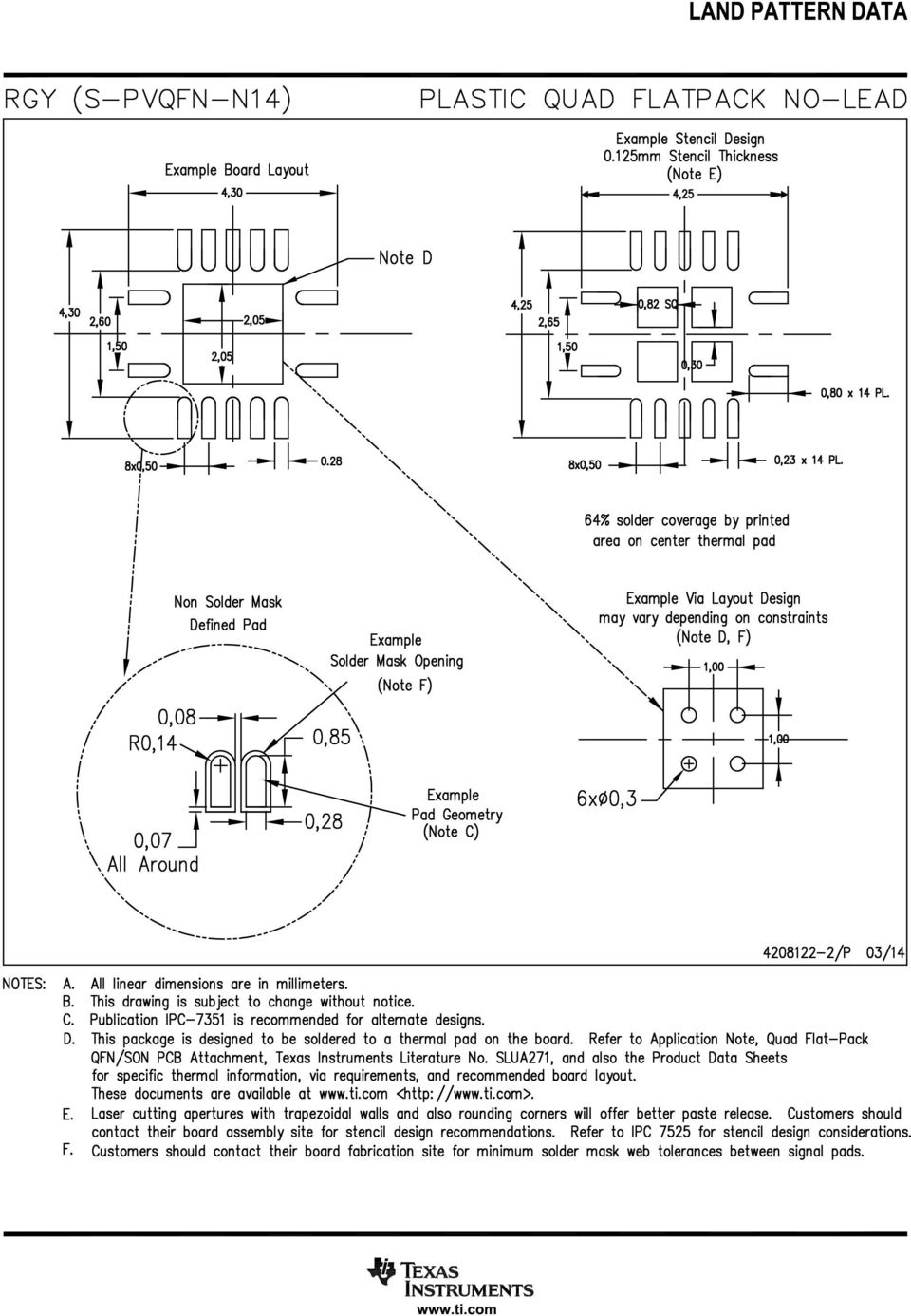
1OE 3B NC 3B V GND ORDERING INFORMATION. QFN RGY Tape and reel SN74CBT3125RGYR CU125. SOIC D Tape and reel SN74CBT3125DR
|
|
|
- Della Fowler
- 7 years ago
- Views:
Transcription
1 SN74CBT3125 QUADRUPLE FET BUS SWITCH SCDS021I MAY 1995 REVISED SEPTEMBER 2002 Standard 125-Type Pinout (D, DB, DGV, and PW Packages) 5-Ω Switch Connection Between Two Ports TTL-Compatible Input Levels D, DB, DGV, OR PW PACKAGE (TOP VIEW) RGY PACKAGE (TOP VIEW) DBQ PACKAGE (TOP VIEW) 1OE 1A 1B 2OE 2A 2B GND V CC 4OE 4A 4B 3OE 3A 3B 1A 1B 2OE 2A 2B OE 3B V GND CC OE 4A 4B 3OE 3A NC 1OE 1A 1B 2OE 2A 2B GND V CC 4OE 4A 4B 3OE 3A 3B NC NC No internal connection description/ordering information The SN74CBT3125 quadruple FET bus switch features independent line switches. Each switch is disabled when the associated output-enable (OE) input is high. To ensure the high-impedance state during power up or power down, OE should be tied to V CC through a pullup resistor; the minimum value of the resistor is determined by the current-sinking capability of the driver. ORDERING INFORMATION T A PACKAGE ORDERABLE TOP-SIDE PART NUMBER MARKING QFN RGY Tape and reel SN74CBT3125RGYR CU125 Tube SN74CBT3125D SOIC D Tape and reel SN74CBT3125DR CBT C to 85 C SSOP DB Tape and reel SN74CBT3125DBR CU125 SSOP (QSOP) DBQ Tape and reel SN74CBT3125DBQR CU125 TSSOP PW Tape and reel SN74CBT3125PWR CU125 TVSOP DGV Tape and reel SN74CBT3125DGVR CU125 Package drawings, standard packing quantities, thermal data, symbolization, and PCB design guidelines are available at FUNCTION TABLE (each bus switch) INPUT FUNCTION OE L A port = B port H Disconnect Please be aware that an important notice concerning availability, standard warranty, and use in critical applications of Texas Instruments semiconductor products and disclaimers thereto appears at the end of this data sheet. PRODUCTION DATA information is current as of publication date. Products conform to specifications per the terms of Texas Instruments standard warranty. Production processing does not necessarily include testing of all parameters. Copyright 2002, Texas Instruments Incorporated POST OFFICE BOX DALLAS, TEXAS
 input is high.")
2 SN74CBT3125 QUADRUPLE FET BUS SWITCH SCDS021I MAY 1995 REVISED SEPTEMBER 2002 logic diagram (positive logic) 1A 2 3 1B 1OE 1 2A 5 6 2B 2OE 4 3A 9 8 3B 3OE 10 4A B 4OE 13 Pin numbers shown are for the D, DB, DGV, PW, and RGY packages. absolute maximum ratings over operating free-air temperature range (unless otherwise noted) Supply voltage range, V CC V to 7 V Input voltage range, V I (see Note 1) V to 7 V Continuous channel current ma Input clamp current, I K (V I/O < 0) ma Package thermal impedance, θ JA (see Note 2): D package C/W (see Note 2): DB package C/W (see Note 2): DBQ package C/W (see Note 2): DGV package C/W (see Note 2): PW package C/W (see Note 3): RGY package C/W Storage temperature range, T stg C to 150 C Stresses beyond those listed under absolute maximum ratings may cause permanent damage to the device. These are stress ratings only, and functional operation of the device at these or any other conditions beyond those indicated under recommended operating conditions is not implied. Exposure to absolute-maximum-rated conditions for extended periods may affect device reliability. NOTES: 1. The input and output negative-voltage ratings may be exceeded if the input and output clamp-current ratings are observed. 2. The package thermal impedance is calculated in accordance with JESD The package thermal impedance is calculated in accordance with JESD recommended operating conditions (see Note 4) MIN MAX UNIT V CC Supply voltage V V IH High-level control input voltage 2 V V IL Low-level control input voltage 0.8 V T A Operating free-air temperature C NOTE 4: All unused control inputs of the device must be held at V CC or GND to ensure proper device operation. Refer to the TI application report, Implications of Slow or Floating CMOS Inputs, literature number SCBA POST OFFICE BOX DALLAS, TEXAS 75265
: D package................................... 86 C/W (see Note 2): DB package.")
3 SN74CBT3125 QUADRUPLE FET BUS SWITCH SCDS021I MAY 1995 REVISED SEPTEMBER 2002 electrical characteristics over recommended operating free-air temperature range (unless otherwise noted) PARAMETER TEST CONDITIONS MIN TYP MAX UNIT V IK V CC = 4 V, I I = 18 ma 1.2 V I I V CC = 5.5 V, V I = 5.5 V or GND ±1 μa I CC V CC = 5.5 V, I O = 0, V I = V CC or GND 3 μa ΔI CC Control inputs V CC = 5.5 V, One input at 3.4 V, Other inputs at V CC or GND 2.5 ma C i Control inputs V I = 3 V or 0 3 pf C io(off) V O = 3 V or 0, OE = V CC 4 pf r on V CC = 4 V, TYP at V CC = 4 V V CC = 4.5 V V I = 2.4 V, I I = 15 ma V I = 0 I I = 64 ma 5 7 Ω I I = 30 ma 5 7 V I = 2.4 V, I I = 15 ma All typical values are at V CC = 5 V (unless otherwise noted), T A = 25 C. This is the increase in supply current for each input that is at the specified TTL voltage level rather than V CC or GND. Measured by the voltage drop between the A and the B terminals at the indicated current through the switch. On-state resistance is determined by the lower voltage of the two (A or B) terminals. switching characteristics over recommended operating free-air temperature range, C L = 50 pf (unless otherwise noted) (see Figure 1) PARAMETER t pd FROM (INPUT) TO (OUTPUT) V V CC = 4 V CC = 5 V ± 0.5 V UNIT MIN MAX MIN MAX A or B B or A ns t en OE A or B ns t dis OE A or B ns The propagation delay is the calculated RC time constant of the typical on-state resistance of the switch and the specified load capacitance, when driven by an ideal voltage source (zero output impedance). POST OFFICE BOX DALLAS, TEXAS
, T A = 25 C.")
4 SN74CBT3125 QUADRUPLE FET BUS SWITCH SCDS021I MAY 1995 REVISED SEPTEMBER 2002 PARAMETER MEASUREMENT INFORMATION From Output Under Test C L = 50 pf (see Note A) 500 Ω 500 Ω S1 7 V Open GND TEST t pd t PLZ /t PZL t PHZ /t PZH S1 Open 7 V Open LOAD CIRCUIT Output Control 1.5 V 1.5 V 3 V 0 V t PZL t PLZ Input 1.5 V 1.5 V 3 V 0 V Output Waveform 1 S1 at 7 V (see Note B) 1.5 V 3.5 V V OL V V OL Output t PLH t PHL 1.5 V 1.5 V V OH V OL Output Waveform 2 S1 at Open (see Note B) t PZH 1.5 V t PHZ V OH V OH 0.3 V 0 V VOLTAGE WAVEFORMS PROPAGATION DELAY TIMES VOLTAGE WAVEFORMS ENABLE AND DISABLE TIMES NOTES: A. C L includes probe and jig capacitance. B. Waveform 1 is for an output with internal conditions such that the output is low except when disabled by the output control. Waveform 2 is for an output with internal conditions such that the output is high except when disabled by the output control. C. All input pulses are supplied by generators having the following characteristics: PRR 10 MHz, Z O = 50 Ω, t r 2.5 ns, t f 2.5 ns. D. The outputs are measured one at a time with one transition per measurement. E. t PLZ and t PHZ are the same as t dis. F. t PZL and t PZH are the same as t en. G. t PLH and t PHL are the same as t pd. H. All parameters and waveforms are not applicable to all devices. Figure 1. Load Circuit and Voltage Waveforms 4 POST OFFICE BOX DALLAS, TEXAS 75265

5 PACKAGE OPTION ADDENDUM 10-Jun-2014 PACKAGING INFORMATION Orderable Device Status (1) Package Type Package Drawing Pins Package Qty Eco Plan SN74CBT3125D ACTIVE SOIC D Green (RoHS (2) Lead/Ball Finish (6) MSL Peak Temp (3) Op Temp ( C) CU NIPDAU Level-1-260C-UNLIM -40 to 85 CBT3125 SN74CBT3125DBLE OBSOLETE SSOP DB 14 TBD Call TI Call TI -40 to 85 SN74CBT3125DBQR ACTIVE SSOP DBQ Green (RoHS SN74CBT3125DBR ACTIVE SSOP DB Green (RoHS SN74CBT3125DBRE4 ACTIVE SSOP DB Green (RoHS SN74CBT3125DG4 ACTIVE SOIC D Green (RoHS SN74CBT3125DGVR ACTIVE TVSOP DGV Green (RoHS SN74CBT3125DR ACTIVE SOIC D Green (RoHS SN74CBT3125PW ACTIVE TSSOP PW Green (RoHS SN74CBT3125PWG4 ACTIVE TSSOP PW Green (RoHS CU NIPDAU Level-2-260C-1 YEAR -40 to 85 CU125 CU NIPDAU Level-1-260C-UNLIM -40 to 85 CU125 CU NIPDAU Level-1-260C-UNLIM -40 to 85 CU125 CU NIPDAU Level-1-260C-UNLIM -40 to 85 CBT3125 CU NIPDAU Level-1-260C-UNLIM -40 to 85 CU125 CU NIPDAU Level-1-260C-UNLIM -40 to 85 CBT3125 CU NIPDAU Level-1-260C-UNLIM -40 to 85 CU125 CU NIPDAU Level-1-260C-UNLIM -40 to 85 CU125 SN74CBT3125PWLE OBSOLETE TSSOP PW 14 TBD Call TI Call TI -40 to 85 SN74CBT3125PWR ACTIVE TSSOP PW Green (RoHS SN74CBT3125PWRE4 ACTIVE TSSOP PW Green (RoHS SN74CBT3125PWRG4 ACTIVE TSSOP PW Green (RoHS SN74CBT3125RGYR ACTIVE VQFN RGY Green (RoHS CU NIPDAU Level-1-260C-UNLIM -40 to 85 CU125 CU NIPDAU Level-1-260C-UNLIM -40 to 85 CU125 CU NIPDAU Level-1-260C-UNLIM -40 to 85 CU125 CU NIPDAU Level-2-260C-1 YEAR -40 to 85 CU125 Device Marking (4/5) Samples (1) The marketing status values are defined as follows: ACTIVE: Product device recommended for new designs. LIFEBUY: TI has announced that the device will be discontinued, and a lifetime-buy period is in effect. NRND: Not recommended for new designs. Device is in production to support existing customers, but TI does not recommend using this part in a new design. PREVIEW: Device has been announced but is not in production. Samples may or may not be available. OBSOLETE: TI has discontinued the production of the device. Addendum-Page 1

6 PACKAGE OPTION ADDENDUM 10-Jun-2014 (2) Eco Plan - The planned eco-friendly classification: Pb-Free (RoHS), Pb-Free (RoHS Exempt), or Green (RoHS - please check for the latest availability information and additional product content details. TBD: The Pb-Free/Green conversion plan has not been defined. Pb-Free (RoHS): TI's terms "Lead-Free" or "Pb-Free" mean semiconductor products that are compatible with the current RoHS requirements for all 6 substances, including the requirement that lead not exceed 0.1% by weight in homogeneous materials. Where designed to be soldered at high temperatures, TI Pb-Free products are suitable for use in specified lead-free processes. Pb-Free (RoHS Exempt): This component has a RoHS exemption for either 1) lead-based flip-chip solder bumps used between the die and package, or 2) lead-based die adhesive used between the die and leadframe. The component is otherwise considered Pb-Free (RoHS compatible) as defined above. Green (RoHS : TI defines "Green" to mean Pb-Free (RoHS compatible), and free of Bromine (Br) and Antimony (Sb) based flame retardants (Br or Sb do not exceed 0.1% by weight in homogeneous material) (3) MSL, Peak Temp. - The Moisture Sensitivity Level rating according to the JEDEC industry standard classifications, and peak solder temperature. (4) There may be additional marking, which relates to the logo, the lot trace code information, or the environmental category on the device. (5) Multiple Device Markings will be inside parentheses. Only one Device Marking contained in parentheses and separated by a "~" will appear on a device. If a line is indented then it is a continuation of the previous line and the two combined represent the entire Device Marking for that device. (6) Lead/Ball Finish - Orderable Devices may have multiple material finish options. Finish options are separated by a vertical ruled line. Lead/Ball Finish values may wrap to two lines if the finish value exceeds the maximum column width. Important Information and Disclaimer:The information provided on this page represents TI's knowledge and belief as of the date that it is provided. TI bases its knowledge and belief on information provided by third parties, and makes no representation or warranty as to the accuracy of such information. Efforts are underway to better integrate information from third parties. TI has taken and continues to take reasonable steps to provide representative and accurate information but may not have conducted destructive testing or chemical analysis on incoming materials and chemicals. TI and TI suppliers consider certain information to be proprietary, and thus CAS numbers and other limited information may not be available for release. In no event shall TI's liability arising out of such information exceed the total purchase price of the TI part(s) at issue in this document sold by TI to Customer on an annual basis. Addendum-Page 2

7 PACKAGE MATERIALS INFORMATION 22-Jan-2015 TAPE AND REEL INFORMATION *All dimensions are nominal Device Package Type Package Drawing Pins SPQ Reel Diameter (mm) Reel Width W1 (mm) A0 (mm) B0 (mm) K0 (mm) P1 (mm) W (mm) Pin1 Quadrant SN74CBT3125DBR SSOP DB Q1 SN74CBT3125DGVR TVSOP DGV Q1 SN74CBT3125DR SOIC D Q1 SN74CBT3125PWR TSSOP PW Q1 SN74CBT3125RGYR VQFN RGY Q1 Pack Materials-Page 1

8 PACKAGE MATERIALS INFORMATION 22-Jan-2015 *All dimensions are nominal Device Package Type Package Drawing Pins SPQ Length (mm) Width (mm) Height (mm) SN74CBT3125DBR SSOP DB SN74CBT3125DGVR TVSOP DGV SN74CBT3125DR SOIC D SN74CBT3125PWR TSSOP PW SN74CBT3125RGYR VQFN RGY Pack Materials-Page 2

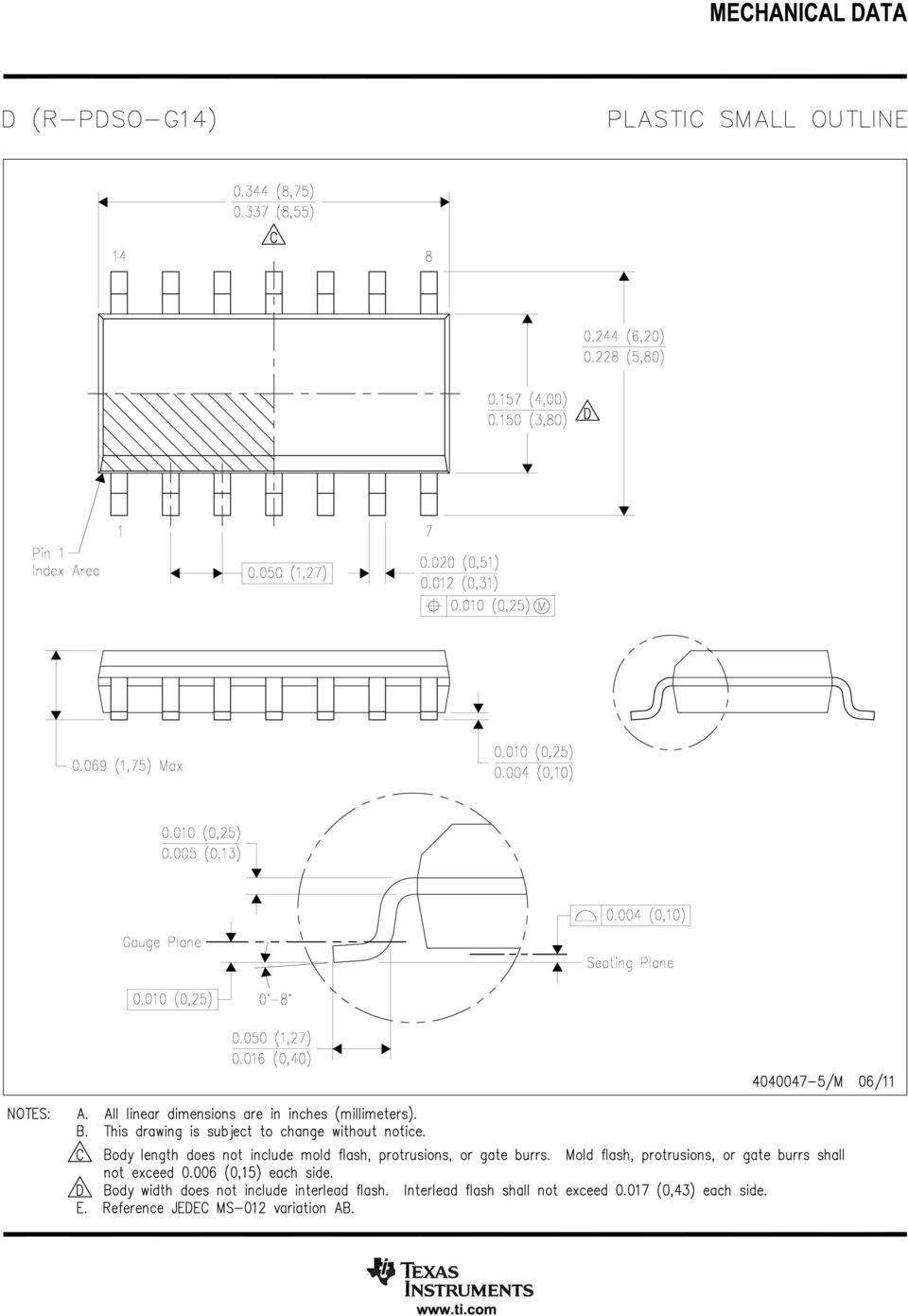
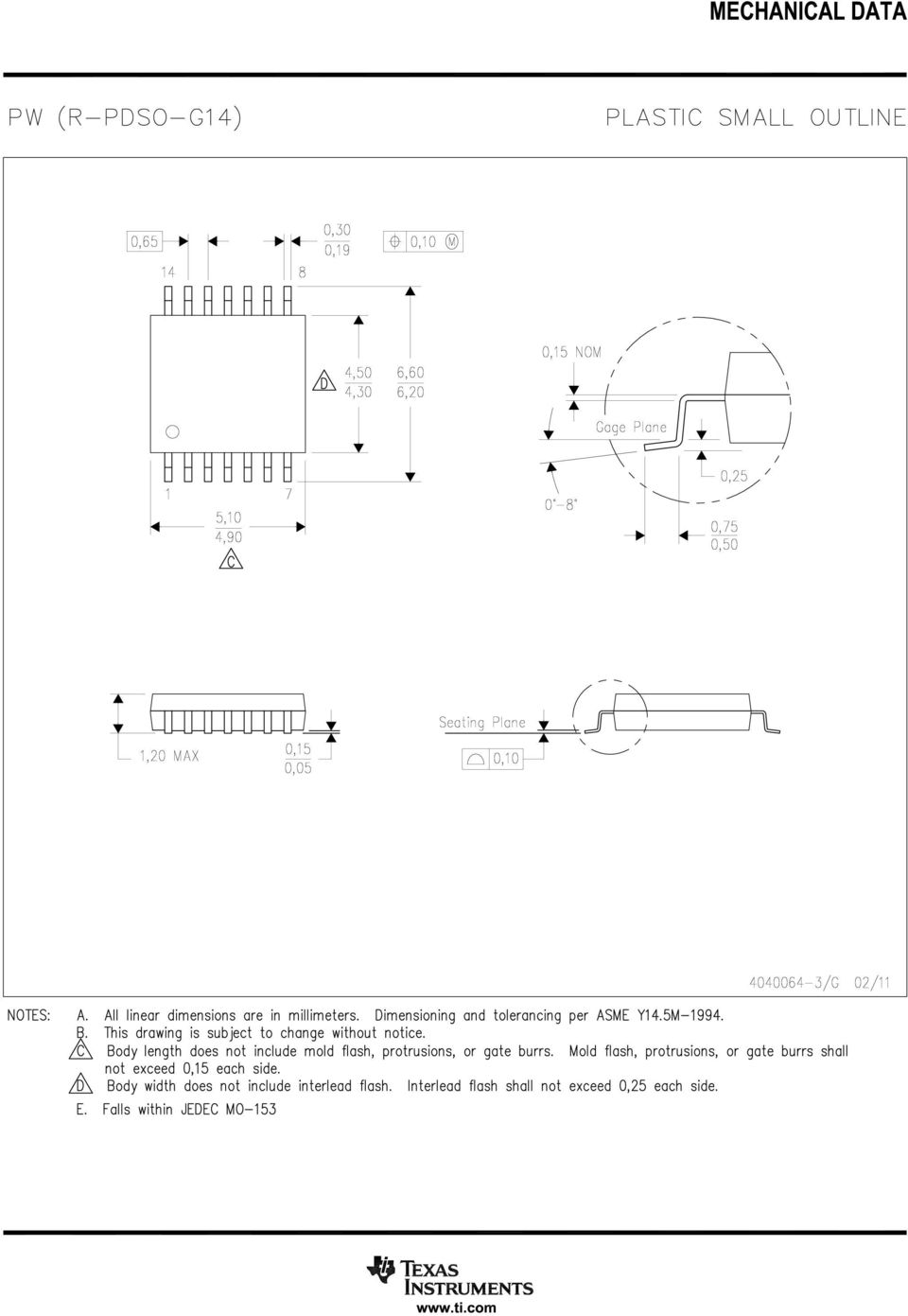
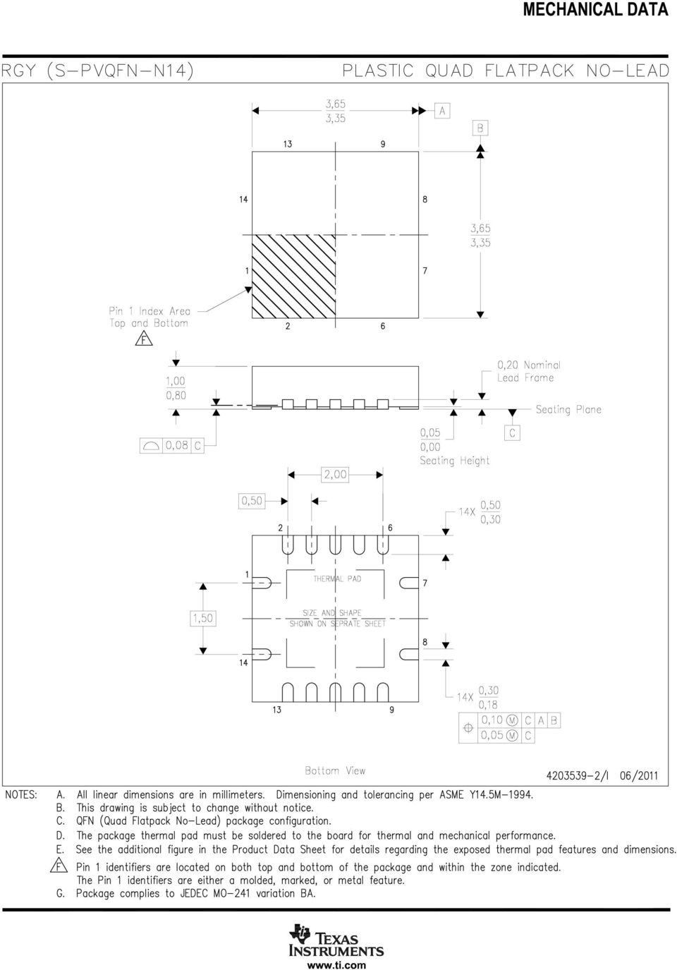
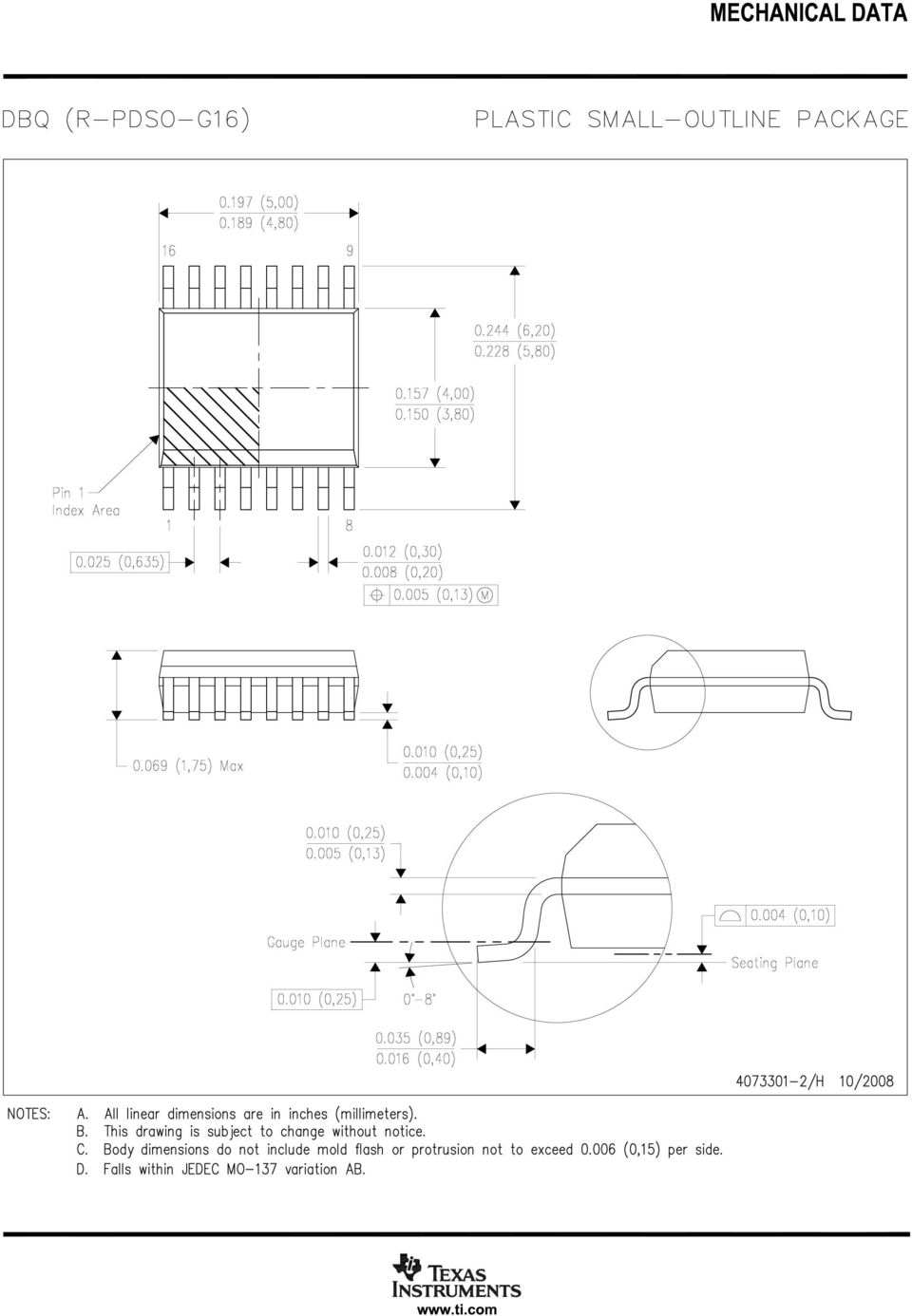
9 MECHANICAL DATA MPDS006C FEBRUARY 1996 REVISED AUGUST 2000 DGV (R-PDSO-G**) 24 PINS SHOWN PLASTIC SMALL-OUTLINE 0,40 0,23 0,13 0,07 M ,16 NOM 4,50 4,30 6,60 6,20 Gage Plane 1 12 A 0 8 0,25 0,75 0,50 1,20 MAX 0,15 0,05 Seating Plane 0,08 DIM PINS ** A MAX 3,70 3,70 5,10 5,10 7,90 9,80 11,40 A MIN 3,50 3,50 4,90 4,90 7,70 9,60 11, /E 08/00 NOTES: A. All linear dimensions are in millimeters. B. This drawing is subject to change without notice. C. Body dimensions do not include mold flash or protrusion, not to exceed 0,15 per side. D. Falls within JEDEC: 24/48 Pins MO /16/20/56 Pins MO-194 POST OFFICE BOX DALLAS, TEXAS 75265

10
11

12
13
14
15

16
17
18

19 MECHANICAL DATA MSSO002E JANUARY 1995 REVISED DECEMBER 2001 DB (R-PDSO-G**) 28 PINS SHOWN PLASTIC SMALL-OUTLINE 0,65 0,38 0,22 0,15 M ,60 5,00 8,20 7,40 0,25 0,09 Gage Plane ,25 A 0 8 0,95 0,55 2,00 MAX 0,05 MIN Seating Plane 0,10 DIM PINS ** A MAX 6,50 6,50 7,50 8,50 10,50 10,50 12,90 A MIN 5,90 5,90 6,90 7,90 9,90 9,90 12, /E 12/01 NOTES: A. All linear dimensions are in millimeters. B. This drawing is subject to change without notice. C. Body dimensions do not include mold flash or protrusion not to exceed 0,15. D. Falls within JEDEC MO-150 POST OFFICE BOX DALLAS, TEXAS 75265

20 IMPORTANT NOTICE Texas Instruments Incorporated and its subsidiaries (TI) reserve the right to make corrections, enhancements, improvements and other changes to its semiconductor products and services per JESD46, latest issue, and to discontinue any product or service per JESD48, latest issue. Buyers should obtain the latest relevant information before placing orders and should verify that such information is current and complete. All semiconductor products (also referred to herein as components ) are sold subject to TI s terms and conditions of sale supplied at the time of order acknowledgment. TI warrants performance of its components to the specifications applicable at the time of sale, in accordance with the warranty in TI s terms and conditions of sale of semiconductor products. Testing and other quality control techniques are used to the extent TI deems necessary to support this warranty. Except where mandated by applicable law, testing of all parameters of each component is not necessarily performed. TI assumes no liability for applications assistance or the design of Buyers products. Buyers are responsible for their products and applications using TI components. To minimize the risks associated with Buyers products and applications, Buyers should provide adequate design and operating safeguards. TI does not warrant or represent that any license, either express or implied, is granted under any patent right, copyright, mask work right, or other intellectual property right relating to any combination, machine, or process in which TI components or services are used. Information published by TI regarding third-party products or services does not constitute a license to use such products or services or a warranty or endorsement thereof. Use of such information may require a license from a third party under the patents or other intellectual property of the third party, or a license from TI under the patents or other intellectual property of TI. Reproduction of significant portions of TI information in TI data books or data sheets is permissible only if reproduction is without alteration and is accompanied by all associated warranties, conditions, limitations, and notices. TI is not responsible or liable for such altered documentation. Information of third parties may be subject to additional restrictions. Resale of TI components or services with statements different from or beyond the parameters stated by TI for that component or service voids all express and any implied warranties for the associated TI component or service and is an unfair and deceptive business practice. TI is not responsible or liable for any such statements. Buyer acknowledges and agrees that it is solely responsible for compliance with all legal, regulatory and safety-related requirements concerning its products, and any use of TI components in its applications, notwithstanding any applications-related information or support that may be provided by TI. Buyer represents and agrees that it has all the necessary expertise to create and implement safeguards which anticipate dangerous consequences of failures, monitor failures and their consequences, lessen the likelihood of failures that might cause harm and take appropriate remedial actions. Buyer will fully indemnify TI and its representatives against any damages arising out of the use of any TI components in safety-critical applications. In some cases, TI components may be promoted specifically to facilitate safety-related applications. With such components, TI s goal is to help enable customers to design and create their own end-product solutions that meet applicable functional safety standards and requirements. Nonetheless, such components are subject to these terms. No TI components are authorized for use in FDA Class III (or similar life-critical medical equipment) unless authorized officers of the parties have executed a special agreement specifically governing such use. Only those TI components which TI has specifically designated as military grade or enhanced plastic are designed and intended for use in military/aerospace applications or environments. Buyer acknowledges and agrees that any military or aerospace use of TI components which have not been so designated is solely at the Buyer's risk, and that Buyer is solely responsible for compliance with all legal and regulatory requirements in connection with such use. TI has specifically designated certain components as meeting ISO/TS16949 requirements, mainly for automotive use. In any case of use of non-designated products, TI will not be responsible for any failure to meet ISO/TS Products Applications Audio Automotive and Transportation Amplifiers amplifier.ti.com Communications and Telecom Data Converters dataconverter.ti.com Computers and Peripherals DLP Products Consumer Electronics DSP dsp.ti.com Energy and Lighting Clocks and Timers Industrial Interface interface.ti.com Medical Logic logic.ti.com Security Power Mgmt power.ti.com Space, Avionics and Defense Microcontrollers microcontroller.ti.com Video and Imaging RFID OMAP Applications Processors TI E2E Community e2e.ti.com Wireless Connectivity Mailing Address: Texas Instruments, Post Office Box , Dallas, Texas Copyright 2015, Texas Instruments Incorporated
 are sold subject to TI s terms and conditions of sale supplied at the time of order acknowledgment.")
Data sheet acquired from Harris Semiconductor SCHS078C -- Revised October 2003
 Data sheet acquired from Harris Semiconductor SCHS078C -- Revised October 2003 The CD4521B types are supplied in 16-lead dual-in-line plastic packages (E suffix), 16-lead small-outline packages (M, M96,
SDLS940A MARCH 1974 REVISED MARCH 1988. Copyright 1988, Texas Instruments Incorporated
 SN5490A, SN5492A, SN5493A, SN54LS90, SN54LS92, SN54LS93 SN7490A, SN7492A, SN7493A, SN74LS90, SN74LS92, SN74LS93 DECADE, DIVIDE-BY-TWELVE AND BINARY COUNTERS SDLS940A MARCH 1974 REVISED MARCH 1988 PRODUCTION
CD4071B Quad 2-Input OR Gate CD4072B Dual 4-Input OR Gate CD4075B Triple 3-Input OR Gate
 Data sheet acquired from Harris Semiconductor SCHS056D Revised August 2003 CD4071B Quad 2-Input OR Gate CD4072B Dual 4-Input OR Gate CD4075B Triple 3-Input OR Gate CD4071B, CD4072B, and CD4075B OR gates
Data sheet acquired from Harris Semiconductor SCHS049C Revised October 2003
 Data sheet acquired from Harris Semiconductor SCHS049C Revised October 2003 CD4060B consists of an oscillator section and 14 ripple-carry binary counter stages. The oscillator configuration allows design
with Ultra-Fast Transient Response and High Light-Load Efficiency
 1 Adaptor 6-24V Optional N-FET Driver Ultra-Fast DPM Simplified Application Diagram Iin Ultra-Low Quiescent Current Enhanced Safety Features OCP, OVP, FET Short Support CPU Turbo Mode To System bq24715
Data sheet acquired from Harris Semiconductor SCHS020C Revised October 2003
 Data sheet acquired from Harris Semiconductor SCHS020C Revised October 2003 The CD4009UB and CD4010B types are supplied in 16-lead hermetic dual-in-line ceramic packages (F3A suffix), 16-lead dual-in-line
Data sheet acquired from Harris Semiconductor SCHS067B Revised July 2003
 Data sheet acquired from Harris Semiconductor SCHS067B Revised July 2003 The CD4502B types are supplied in 16-lead hermetic dual-in-line ceramic packages (F3A suffix), 16-lead dual-in-line plastic packages
SN54LVT574, SN74LVT574 3.3-V ABT OCTAL EDGE-TRIGGERED D-TYPE FLIP-FLOPS WITH 3-STATE OUTPUTS
 SN54LVT574, SN74LVT574 3.3-V ABT OCTAL EDGE-TRIGGERED D-TYPE FLIP-FLOPS WITH 3-STATE OUTPUTS SCBS139D MAY 1992 REVISED JULY 1995 State-of-the-Art Advanced BiCMOS Technology (ABT) Design for 3.3-V Operation
ESD Protection Exceeds JESD 22 I off. 2000-V Human-Body Model (A114-A) 200-V Machine Model (A115-A)
 200-V Machine Model (A115-A)") www.ti.com FEATURES SN74CBTLV3245A LOW-VOLTAGE OCTAL FET BUS SWITCH SCDS034M JULY 1997 REVISED AUGUST 2005 Standard '245-Type Pinout Latch-Up Performance Exceeds 250 ma Per 5-Ω Switch Connection Between
www.ti.com FEATURES SN74CBTLV3245A LOW-VOLTAGE OCTAL FET BUS SWITCH SCDS034M JULY 1997 REVISED AUGUST 2005 Standard '245-Type Pinout Latch-Up Performance Exceeds 250 ma Per 5-Ω Switch Connection Between
Data sheet acquired from Harris Semiconductor SCHS087D Revised October 2003
 Data sheet acquired from Harris Semiconductor SCHS087D Revised October 2003 The CD4555B and CD4556B types are supplied in 16-lead hermetic dual-in-line ceramic packages (F3A suffix), 16-lead dual-in-line
 PACKAGE OPTION ADDENDUM www.ti.com 12-Jan-2006 PACKAGING INFORMATION Orderable Device Status (1) Package Type Package Drawing Pins Package Qty Eco Plan (2) Lead/Ball Finish MSL Peak Temp (3) 5962-9557401QCA
 PACKAGE OPTION ADDENDUM www.ti.com 12-Jan-2006 PACKAGING INFORMATION Orderable Device Status (1) Package Type Package Drawing Pins Package Qty Eco Plan (2) Lead/Ball Finish MSL Peak Temp (3) 76005012A
ORDERING INFORMATION. TOP-SIDE MARKING PDIP N Tube SN74LS07N SN74LS07N PACKAGE. SOIC D Tape and reel SN74LS07DR
 The SN54LS07 and SN74LS17 are obsolete and are no longer supplied. Convert TTL Voltage Levels to MOS Levels High Sink-Current Capability Input Clamping Diodes Simplify System Design Open-Collector Driver
RF37S114 Tag-it HF-I Type 5 NFC, ISO/IEC 15693 Transponder, 4 mm 4 mm
 1 1 Product Folder Sample & Buy Technical Documents Tools & Software Support & Community RF37S114 SCBS907 NOVEMBER 2015 RF37S114 Tag-it HF-I Type 5 NFC, ISO/IEC 15693 Transponder, 4 mm 4 mm 1 Device Overview
PACKAGE OPTION ADDENDUM
 PACKAGE OPTION ADDENDUM www.ti.com 10-Jun-2014 PACKAGING INFORMATION Orderable Device Status (1) Package Type Package Drawing Pins Package Qty Eco Plan (2) Lead/Ball Finish (6) MSL Peak Temp (3) Op Temp
SN54HC574, SN74HC574 OCTAL EDGE-TRIGGERED D-TYPE FLIP-FLOPS WITH 3-STATE OUTPUTS
 Wide Operating Voltage Range of 2 V to 6 V High-Current 3-State Noninverting Outputs Drive Bus Lines Directly or Up To 15 LSTTL Loads Low Power Consumption, 80-μA Max I CC Typical t pd = 22 ns ±6-mA Output
LM556 LM556 Dual Timer
 LM556 LM556 Dual Timer Literature Number: SNAS549 LM556 Dual Timer General Description The LM556 Dual timing circuit is a highly stable controller capable of producing accurate time delays or oscillation.
LM5030 LM5030 Application: DC - DC Converter Utilizing the Push-Pull Topology
 LM5030 LM5030 Application: DC - DC Converter Utilizing the Push-Pull Topology Literature Number: SNVA553 LM5030 Application DC DC Converter Utilizing the Push-Pull Topology 1 Push-Pull Topology D1 L +
SN54LV163A, SN74LV163A 4-BIT SYNCHRONOUS BINARY COUNTERS
 SN54LV163A, SN74LV163A 4-BIT SYNCHRONOUS BINARY COUNTERS 2-V to 5.5-V V CC Operation Max t pd of 9.5 ns at 5 V Typical V OLP (Output Ground Bounce)
Application Note AN107
 Murata Balun for CC253x and CC254x LFB182G45BG2D280 By Fredrik Kervel Keywords Balun LFB182G45BG2D280 CC253x CC254x CC257x CC85xx 1 Introduction Murata s LFB182G45BG2D280 integrated balun is specially
AMC1100: Replacement of Input Main Sensing Transformer in Inverters with Isolated Amplifier
 Application Report SLAA552 August 2012 AMC1100: Replacement of Input Main Sensing Transformer in Inverters with Isolated Amplifier Ambreesh Tripathi and Harmeet Singh Analog/Digital Converters ABSTRACT
54LS174,54LS175,DM54LS174,DM54LS175, DM74LS174,DM74LS175
 54LS174,54LS175,DM54LS174,DM54LS175, DM74LS174,DM74LS175 54LS174 DM54LS174 DM74LS174 54LS175 DM54LS175 DM74LS175 Hex/Quad D Flip-Flops with Clear Literature Number: SNOS290A 54LS174 DM54LS174 DM74LS174
description/ordering information
 SCES207I APRIL 1999 REVISED SEPTEMBER 2003 Available in the Texas Instruments NanoStar and NanoFree Packages Supports 5-V V CC Operation Inputs Accept Voltages to 5.5 V Max t pd of 6 ns at 3.3 V Low Power
LM709 LM709 Operational Amplifier
 LM709 LM709 Operational Amplifier Literature Number: SNOS659A LM709 Operational Amplifier General Description The LM709 series is a monolithic operational amplifier intended for general-purpose applications
description typical application
 Overvoltage Protection and Lockout for 12 V, 5 V, 3.3 V Undervoltage Protection and Lockout for 5 V and 3.3 V Fault Protection Output With Open-Drain Output Stage Open-Drain Power Good Output Signal for
description/ordering information
 SLLS047L FEBRUARY 1989 REVISED MARCH 2004 Meets or Exceeds TIA/EIA-232-F and ITU Recommendation V.28 Operates From a Single 5-V Power Supply With 1.0-F Charge-Pump Capacitors Operates Up To 120 kbit/s
CD4051B-Q1, CD4052B-Q1, CD4053B-Q1 CMOS ANALOG MULTIPLEXERS/DEMULTIPLEXERS WITH LOGIC LEVEL CONVERSION
 Features Qualified for Automotive Applications Wide Range of Digital and Analog Signal Levels Digital: V to 0 V Analog: 0 V P-P Low ON Resistance, Ω (Typ) Over V P-P Signal Input Range for = V High OFF
µa7800 SERIES POSITIVE-VOLTAGE REGULATORS
 SLS056J MAY 976 REISED MAY 2003 3-Terminal Regulators Output Current up to.5 A Internal Thermal-Overload Protection High Power-Dissipation Capability Internal Short-Circuit Current Limiting Output Transistor
SN54ABT377, SN74ABT377A OCTAL EDGE-TRIGGERED D-TYPE FLIP-FLOPS WITH CLOCK ENABLE
 State-of-the-Art EPIC-ΙΙB BiCMOS Design Significantly Reduces Power Dissipation Latch-Up Performance Exceeds 500 ma Per JEDEC Standard JESD-17 Typical V OLP (Output Ground Bounce) < 1 V at V CC = 5 V,
SN55115, SN75115 DUAL DIFFERENTIAL RECEIVERS
 SN55115, SN75115 DUAL DIFFERENTIAL RECEIVERS Choice of Open-Collector or Active Pullup (Totem-Pole) Outputs Single 5-V Supply Differential Line Operation Dual-Channel Operation TTL Compatible ± 15-V Common-Mode
TMP100 EP DIGITAL TEMPERATURE SENSOR WITH I 2 C INTERFACE
 Controlled Baseline One Assembly/Test Site, One Fabrication Site Enhanced Diminishing Manufacturing Sources (DMS) Support Enhanced Product-Change Notification Qualification Pedigree Digital Output: I 2
description V CC A CLR BO CO LOAD C D B Q B Q A DOWN UP Q C Q D GND D OR N PACKAGE (TOP VIEW) SDFS031A D3693, JANUARY 1991 REVISED OCTOBER 1993
 SDFS031A D3693, JANUARY 1991 REVISED OCTOBER 1993") High-Speed f max of 100 MHz Typical Parallel Asynchronous Load for Modulo-N Count Lengths Look-Ahead Circuitry Enhances Speed of Cascaded Counters Fully Synchronous in Count Modes Package Optio Include
High-Speed f max of 100 MHz Typical Parallel Asynchronous Load for Modulo-N Count Lengths Look-Ahead Circuitry Enhances Speed of Cascaded Counters Fully Synchronous in Count Modes Package Optio Include
Analysis of Power Supply Topologies for IGBT Gate Drivers in Industrial
 Application Report SLAA672 July 2015 Analysis of Power Supply Topologies for IGBT Gate Drivers in Industrial Sanjay Pithadia, N. Navaneeth Kumar ABSTRACT This application report explains different parameters
FEATURES APPLICATIONS
 FEATURES DIGITALLY-CONTROLLED ANALOG VOLUME CONTROL: Four Independent Audio Channels Serial Control Interface Zero Crossing Detection Mute Function WIDE GAIN AND ATTENUATION RANGE: +31.5dB to 95.5dB with
Design Note DN304. Cebal CCxxxx Development Tools USB Driver Installation Guide By Åsmund B. Bø. Keywords. 1 Introduction
 Cebal CCxxxx Development Tools USB Driver Installation Guide By Åsmund B. Bø Keywords Cebal Driver Windows x86 Windows x64 SmartRF Studio SmartRF Packet Sniffer SmartRF Flash Programmer SmartRF05EB SmartRF04EB
LM388 LM388 1.5W Audio Power Amplifier
 LM388 LM388 1.5W Audio Power Amplifier Literature Number: SNOSBT8A LM388 1 5W Audio Power Amplifier General Description The LM388 is an audio amplifier designed for use in medium power consumer applications
AUDIO DIFFERENTIAL LINE RECEIVER. 0dB (G = 1)
") INA4 INA4 INA4 INA4 INA4 INA4 AUDIO DIFFERENTIAL LINE RECEIVERS db (G = ) FEATURES SINGLE AND DUAL VERSIONS LOW DISTORTION:.% at f = khz HIGH SLEW RATE: 4V/µs FAST SETTLING TIME: µs to.% WIDE SUPPLY RANGE:
INA4 INA4 INA4 INA4 INA4 INA4 AUDIO DIFFERENTIAL LINE RECEIVERS db (G = ) FEATURES SINGLE AND DUAL VERSIONS LOW DISTORTION:.% at f = khz HIGH SLEW RATE: 4V/µs FAST SETTLING TIME: µs to.% WIDE SUPPLY RANGE:
Providing Continuous Gate Drive Using a Charge Pump
 Application Report Philip Meyer and John Tucker... Power Management Products ABSTRACT Certain applications require that output voltage regulation be maintained when the input voltage is only slightly higher
AN-1733 Load Transient Testing Simplified
 Application Report... ABSTRACT The load transient test may be the simplest diagnostic tool available to instantly analyze the loop stability of a system: the visual appearance of the output voltage as
SN54HC157, SN74HC157 QUADRUPLE 2-LINE TO 1-LINE DATA SELECTORS/MULTIPLEXERS
 SNHC, SNHC QUADRUPLE 2-LINE TO -LINE DATA SELECTORS/MULTIPLEXERS SCLSB DECEMBER 982 REVISED MAY 99 Package Options Include Plastic Small-Outline (D) and Ceramic Flat (W) Packages, Ceramic Chip Carriers
DS8907 DS8907 AM/FM Digital Phase-Locked Loop Frequency Synthesizer
 DS8907 DS8907 AM/FM Digital Phase-Locked Loop Frequency Synthesizer Literature Number: SNOSBR1A DS8907 AM FM Digital Phase-Locked Loop Frequency Synthesizer General Description The DS8907 is a PLL synthesizer
CD4049UB, CD4050B. CMOS Hex Buffer/Converters. Applications. [ /Title (CD40 49UB, CD405 0B) /Subject. Ordering Information
 /Subject. Ordering Information") CD4049UB, CD4050B Data sheet acquired from Harris Semiconductor SCHS046I August 1998 - Revised May 2004 [ /Title (CD40 49UB, CD405 0B) /Subject (CMO S Hex Buffer/ Converters) /Autho r () /Keywords (Harris
CD4049UB, CD4050B Data sheet acquired from Harris Semiconductor SCHS046I August 1998 - Revised May 2004 [ /Title (CD40 49UB, CD405 0B) /Subject (CMO S Hex Buffer/ Converters) /Autho r () /Keywords (Harris
TLC556, TLC556Y DUAL LinCMOS TIMERS
 TLC556, TLC556Y DUAL LinCMOS TIMERS ery Low Power Consumption...2 mw Typ at DD = 5 Capable of Operation in Astable Mode CMOS Output Capable of Swinging Rail to Rail High Output-Current Capability Sink
8-bit binary counter with output register; 3-state
 Rev. 3 24 February 2016 Product data sheet 1. General description The is an 8-bit binary counter with a storage register and 3-state outputs. The storage register has parallel (Q0 to Q7) outputs. The binary
Importing a SPICE NetList Into TINA9-TI
 Application Report Importing a SPICE NetList into TINA9-TI John Miller... Analog elab ABSTRACT This application note describes the procedure for importing an unencrypted SPICE netlist into TINA9-TI (available
SN74ACT7808 2048 9 STROBED FIRST-IN, FIRST-OUT MEMORY
 Load Clocks and Unload Clocks Can Be Asynchronous or Coincident 2048 Words by 9 Bits Low-Power Advanced CMOS Technology Fast Access Times of 5 ns With a 50-pF Load Programmable Almost-Full/Almost-Empty
74HC574; 74HCT574. Octal D-type flip-flop; positive edge-trigger; 3-state
 Rev. 7 4 March 2016 Product data sheet 1. General description 2. Features and benefits 3. Ordering information The is an 8-bit positive-edge triggered D-type flip-flop with 3-state outputs. The device
Wireless Subwoofer TI Design Tests
 Wireless Subwoofer TI Design Tests This system design was tested for THD+N vs. frequency at 5 watts and 30 watts and THD+N vs. power at 00. Both the direct analog input and the wireless systems were tested.
Ultrasonic Sensing Basics for Liquid Level Sensing, Flow Sensing, and Fluid
 Application Report SNAA0A March 015 Revised June 015 Ultrasonic Sensing Basics for Liquid Level Sensing, Flow Sensing, and Fluid AmyLe ABSTRACT The need for accurate and reliable sensors is growing in
LM138,LM338. LM138/LM338 5-Amp Adjustable Regulators. Literature Number: SNVS771A
 LM138,LM338 LM138/LM338 5-Amp Adjustable Regulators Literature Number: SNVS771A LM138/LM338 5-Amp Adjustable Regulators General Description The LM138 series of adjustable 3-terminal positive voltage regulators
High-Speed, Low r ON, SPST Analog Switch (1-Bit Bus Switch)
") High-Speed, Low r ON, SPST Analog Switch (1-Bit Bus Switch) DG2301 ishay Siliconix DESCRIPTION The DG2301 is a high-speed, 1-bit, low power, TTLcompatible bus switch. Using sub-micron CMOS technology,
High-Speed, Low r ON, SPST Analog Switch (1-Bit Bus Switch) DG2301 ishay Siliconix DESCRIPTION The DG2301 is a high-speed, 1-bit, low power, TTLcompatible bus switch. Using sub-micron CMOS technology,
DG2302. High-Speed, Low r ON, SPST Analog Switch. Vishay Siliconix. (1-Bit Bus Switch with Level-Shifter) RoHS* COMPLIANT DESCRIPTION FEATURES
 RoHS* COMPLIANT DESCRIPTION FEATURES") High-Speed, Low r ON, SPST Analog Switch (1-Bit Bus Switch with Level-Shifter) DG2302 DESCRIPTION The DG2302 is a high-speed, 1-bit, low power, TTLcompatible bus switch. Using sub-micron CMOS technology,
High-Speed, Low r ON, SPST Analog Switch (1-Bit Bus Switch with Level-Shifter) DG2302 DESCRIPTION The DG2302 is a high-speed, 1-bit, low power, TTLcompatible bus switch. Using sub-micron CMOS technology,
Multi-Transformer LED TV Power User Guide. Anderson Hsiao
 Multi-Transformer LED TV Power User Guide Anderson Hsiao Operation Range Input Range: 90Vac~264Vac 47Hz~63Hz Dimming Range: Reverse Signal 0V ~ 5V 100Hz ~200Hz 1%~100% Output Range :STBY-5V 20mA~1A 5V
V OUT. I o+ & I o- (typical) 2.3A & 3.3A. Package Type
 2.3A & 3.3A. Package Type") July 25 th, 2012 Automotive Grade AUIRS4427S DUAL LOW SIDE DRIVER Features Gate drive supply range from 6 V to 20 V CMOS Schmitt-triggered inputs 3.3V and 5V logic compatible Two independent gate drivers
July 25 th, 2012 Automotive Grade AUIRS4427S DUAL LOW SIDE DRIVER Features Gate drive supply range from 6 V to 20 V CMOS Schmitt-triggered inputs 3.3V and 5V logic compatible Two independent gate drivers
SN55LBC176, SN65LBC176, SN65LBC176Q, SN75LBC176 DIFFERENTIAL BUS TRANSCEIVERS
 Bidirectional Transceiver Meets or Exceeds the Requirements of ANSI Standard TIA/EIA 485 A and ISO 8482:1987(E) High-Speed Low-Power LinBiCMOS Circuitry Designed for High-Speed Operation in Both Serial
TLC548C, TLC548I, TLC549C, TLC549I 8-BIT ANALOG-TO-DIGITAL CONVERTERS WITH SERIAL CONTROL
 Microprocessor Peripheral or Standalone Operation 8-Bit Resolution A/D Converter Differential Reference Input Voltages Conversion Time...17 µs Max Total Access and Conversion Cycles Per Second TLC548...up
Texas Instruments. FB PS LLC Test Report HVPS SYSTEM AND APPLICATION TEAM REVA
 Texas Instruments FB PS LLC Test Report HVPS SYSTEM AND APPLICATION TEAM REVA 12/05/2014 1 General 1.1 PURPOSE Provide the detailed data for evaluating and verifying the FB-PS-LLC. The FB-PS-LLC is a Full
SN74ACT7807 2048 9 CLOCKED FIRST-IN, FIRST-OUT MEMORY
 Free-Running Read and Write Clocks Can Be Asynchronous or Coincident Read and Write Operations Synchronized to Independent System Clocks Input-Ready Flag Synchronized to Write Clock Output-Ready Flag Synchronized
Regulating Pulse Width Modulator
 Regulating Pulse Width Modulator UC1526 FEATURES 8 To 35V Operation 5V Reference Trimmed To ±1% 1Hz To 400kHz Oscillator Range Dual 100mA Source/Sink Outputs Digital Current Limiting Double Pulse Suppression
8-channel analog multiplexer/demultiplexer
 Rev. 12 25 March 2016 Product data sheet 1. General description The is an with three address inputs (S1 to S3), an active LOW enable input (E), eight independent inputs/outputs (Y0 to Y7) and a common
Design Note DN041. Using CC253X or CC254X with Dipole PCB Antennas. Keywords. 1 Introduction. By Espen Wium CC2530 CC2531 CC2533 CC2540 CC2541
 Using CC253X or CC254X with Dipole PCB Antennas By Espen Wium Keywords Half wave dipole RF Antenna Efficiency Gain TRP (Total Radiated Power) CC2530 CC2531 CC2533 CC2540 CC2541 1 Introduction Many RFICs
74HC02; 74HCT02. 1. General description. 2. Features and benefits. Ordering information. Quad 2-input NOR gate
 Rev. 5 26 November 2015 Product data sheet 1. General description 2. Features and benefits The is a quad 2-input NOR gate. Inputs include clamp diodes. This enables the use of current limiting resistors
74HC107; 74HCT107. Dual JK flip-flop with reset; negative-edge trigger
 Rev. 5 30 November 2015 Product data sheet 1. General description 2. Features and benefits 3. Ordering information The is a dual negative edge triggered JK flip-flop featuring individual J and K inputs,
Stereo Audio Volume Control
 PGA2320 Stereo Audio Volume Control FEATURES DIGITALLY-CONTROLLED ANALOG VOLUME CONTROL: Two Independent Audio Channels Serial Control Interface Zero Crossing Detection Mute Function WIDE GAIN AND ATTENUATION
AN-311 Theory and Applications of Logarithmic Amplifiers
 Application Report... ABSTRACT A number of instrumentation applications can benefit from the use of logarithmic or exponential signal processing techniques. The design and use of logarithmic/exponential
Triple single-pole double-throw analog switch
 Rev. 12 25 March 2016 Product data sheet 1. General description 2. Features and benefits 3. Applications 4. Ordering information The is a triple single-pole double-throw (SPDT) analog switch, suitable
74HCU04. 1. General description. 2. Features and benefits. 3. Ordering information. Hex unbuffered inverter
 Rev. 7 8 December 2015 Product data sheet 1. General description The is a hex unbuffered inverter. Inputs include clamp diodes. This enables the use of current limiting resistors to interface inputs to
Application Report. 1 Description of the Problem. Jeff Falin... PMP Portable Power Applications ABSTRACT
 Application Report SLVA255 September 2006 Minimizing Ringing at the Switch Node of a Boost Converter Jeff Falin... PMP Portable Power Applications ABSTRACT This application report explains how to use proper
AN-225 IC Temperature Sensor Provides Thermocouple Cold-Junction
 Application Report AN-225 IC Temperature Sensor Provides Thermocouple Cold-Junction... ABSTRACT Two circuits using the LM335 for thermocouple cold-junction compensation have been described. With a single
74HC138; 74HCT138. 3-to-8 line decoder/demultiplexer; inverting
 Rev. 6 28 December 2015 Product data sheet 1. General description 2. Features and benefits 3. Ordering information The decodes three binary weighted address inputs (A0, A1 and A2) to eight mutually exclusive
74HC154; 74HCT154. 4-to-16 line decoder/demultiplexer
 Rev. 7 29 February 2016 Product data sheet 1. General description 2. Features and benefits 3. Ordering information The is a. It decodes four binary weighted address inputs (A0 to A3) to sixteen mutually
3-to-8 line decoder, demultiplexer with address latches
 Rev. 7 29 January 2016 Product data sheet 1. General description The is a high-speed Si-gate CMOS device and is pin compatible with low-power Schottky TTL (LSTTL). The is specified in compliance with JEDEC
74HC573; 74HCT573. 1. General description. 2. Features and benefits. Octal D-type transparent latch; 3-state
 Rev. 7 4 March 2016 Product data sheet 1. General description The is an 8-bit D-type transparent latch with 3-state outputs. The device features latch enable (LE) and output enable (OE) inputs. When LE
LMS8117A LMS8117A 1A Low-Dropout Linear Regulator
 LMS8117A LMS8117A 1A Low-Dropout Linear Regulator Literature Number: SNOS487E LMS8117A 1A Low-Dropout Linear Regulator General Description The LMS8117A is a series of low dropout voltage regulators with
Hex buffer with open-drain outputs
 Rev. 5 27 October 20 Product data sheet. General description The provides six non-inverting buffers. The outputs are open-drain and can be connected to other open-drain outputs to implement active-low
HEF4011B. 1. General description. 2. Features and benefits. 3. Ordering information. 4. Functional diagram. Quad 2-input NAND gate
 Rev. 6 10 December 2015 Product data sheet 1. General description 2. Features and benefits 3. Ordering information The is a quad 2-input NAND gate. The outputs are fully buffered for the highest noise
INTEGRATED CIRCUITS. 74LVC08A Quad 2-input AND gate. Product specification IC24 Data Handbook. 1997 Jun 30
 INTEGRATED CIRCUITS IC24 Data Handbook 1997 Jun 30 FEATURES Wide supply voltage range of 1.2 V to 3.6 V In accordance with JEDEC standard no. 8-1A Inputs accept voltages up to 5.5 V CMOS low power consumption
74HC595; 74HCT595. 1. General description. 2. Features and benefits. 3. Applications
 8-bit serial-in, serial or parallel-out shift register with output latches; 3-state Rev. 8 25 February 2016 Product data sheet 1. General description The is an 8-bit serial-in/serial or parallel-out shift
3V Video Amplifier with 6dB Gain and Filter in SC70
 OPA360 SB0S294E DECEMBER 2003 REVISED SEPTEMBER 2006 3V Video Amplifier with 6dB Gain and Filter in SC70 FEATURES EXCELLENT VIDEO PERFORMANCE INTERNAL GAIN: 6dB 2-POLE RECONSTRUCTION FILTER SAG CORRECTION
SN54HC191, SN74HC191 4-BIT SYNCHRONOUS UP/DOWN BINARY COUNTERS
 Single Down/Up Count-Control Line Look-Ahead Circuitry Enhances Speed of Cascaded Counters Fully Synchronous in Count Modes Asynchronously Presettable With Load Control Package Options Include Plastic
AVAILABLE OPTIONS SMALL OUTLINE (D)
") SLOS65D MARCH 1991 REVISED APRIL 22 2.5-V Virtual Ground for 5-V/GND Analog Systems High Output-Current Capability Sink or Source... 2 ma Typ Micropower Operation... 17 µa Typ Excellent Regulation Characteristics
SLOS65D MARCH 1991 REVISED APRIL 22 2.5-V Virtual Ground for 5-V/GND Analog Systems High Output-Current Capability Sink or Source... 2 ma Typ Micropower Operation... 17 µa Typ Excellent Regulation Characteristics
4-bit binary full adder with fast carry CIN + (A1 + B1) + 2(A2 + B2) + 4(A3 + B3) + 8(A4 + B4) = = S1 + 2S2 + 4S3 + 8S4 + 16COUT
 + 2(A2 + B2) + 4(A3 + B3) + 8(A4 + B4) = = S1 + 2S2 + 4S3 + 8S4 + 16COUT") Rev. 03 11 November 2004 Product data sheet 1. General description 2. Features The is a high-speed Si-gate CMOS device and is pin compatible with low power Schottky TTL (LSTTL). The is specified in compliance
Rev. 03 11 November 2004 Product data sheet 1. General description 2. Features The is a high-speed Si-gate CMOS device and is pin compatible with low power Schottky TTL (LSTTL). The is specified in compliance
74HC238; 74HCT238. 3-to-8 line decoder/demultiplexer
 Rev. 4 27 January 2016 Product data sheet 1. General description 2. Features and benefits 3. Ordering information The decodes three binary weighted address inputs (A0, A1 and A2) to eight mutually exclusive
74HC377; 74HCT377. 1. General description. 2. Features and benefits. 3. Ordering information
 Rev. 4 24 February 2016 Product data sheet 1. General description 2. Features and benefits 3. Ordering information The is an octal positive-edge triggered D-type flip-flop. The device features clock (CP)
1-of-4 decoder/demultiplexer
 Rev. 6 1 April 2016 Product data sheet 1. General description 2. Features and benefits 3. Applications The contains two 1-of-4 decoders/demultiplexers. Each has two address inputs (na0 and na1, an active
FEATURES DESCRIPTION. www.ti.com SLUS247F APRIL 1997 REVISED NOVEMBER 2007 VDD 8 POWER TO CIRCUITRY. 400 na RES POWER ON RESET 1.
 SLUS247F APRIL 1997 REVISED NOVEMBER 2007 FEATURES Fully Programmable Reset Threshold Fully Programmable Reset Period Fully Programmable Watchdog Period 2% Accurate Reset Threshold Input Voltage Down to
TPS76901, TPS76912, TPS76915, TPS76918, TPS76925 TPS76927, TPS76928, TPS76930, TPS76933, TPS76950 ULTRALOW-POWER 100-mA LOW-DROPOUT LINEAR REGULATORS
 -ma Low-Dropout Regulator TPS76901, TPS76912, TPS76915, TPS76918, TPS76925 TPS76927, TPS76928, TPS76930,, TPS76950 ULTRALOW-POWER -ma LOW-DROPOUT LINEAR REGULATORS Available in 1.2-V, 1.5-V, 1.8-V, 2.5-V,
AN-1963 IEEE 1588 Synchronization Over Standard Networks Using the
 Application Report AN-963 IEEE 588 Synchronization Over Standard Networks Using the... ABSTRACT This application report describes a method of synchronization that provides much more accurate synchronization
DC/DC LED Lighting Developer s Kit Hardware
 Reference Guide The DC/DC LED lighting developer s kit provides a great way to learn and experiment by using a single MCU to accurately control a series of LED strings and efficiently control the power
The 74LVC1G11 provides a single 3-input AND gate.
 Rev. 8 17 September 2015 Product data sheet 1. General description The provides a single 3-input AND gate. The input can be driven from either 3.3 V or 5 V devices. This feature allows the use of this
LM1851 LM1851 Ground Fault Interrupter
 LM1851 LM1851 Ground Fault Interrupter Literature Number: SNIS158 LM1851 Ground Fault Interrupter General Description The LM1851 is designed to provide ground fault protection for AC power outlets in consumer
HEF4021B. 1. General description. 2. Features and benefits. 3. Ordering information. 8-bit static shift register
 Rev. 10 21 March 2016 Product data sheet 1. General description 2. Features and benefits 3. Ordering information The is an (parallel-to-serial converter) with a synchronous serial data input (DS), a clock
Bus buffer/line driver; 3-state
 Rev. 11 2 July 2012 Product data sheet 1. General description The provides one non-inverting buffer/line driver with 3-state output. The 3-state output is controlled by the output enable input (OE). HIGH-level
AN-1405 DP83848 Single 10/100 Mb/s Ethernet Transceiver Reduced Media Independent Interface (RMII ) Mode
 Mode") Application Report SNLA076A October 2005 Revised April 2013 AN-1405 DP83848 Single 10/100 Mb/s Ethernet Transceiver Reduced Media... ABSTRACT This application report summarizes how a designer can take
Application Report SNLA076A October 2005 Revised April 2013 AN-1405 DP83848 Single 10/100 Mb/s Ethernet Transceiver Reduced Media... ABSTRACT This application report summarizes how a designer can take
TL081 TL081 Wide Bandwidth JFET Input Operational Amplifier
 TL081 TL081 Wide Bandwidth JFET Input Operational Amplifier Literature Number: SNOSBW6A TL081 Wide Bandwidth JFET Input Operational Amplifier General Description The TL081 is a low cost high speed JFET
APPLICATION NOTE BUILDING A QAM MODULATOR USING A GC2011 DIGITAL FILTER CHIP
 SLWA022 APPLICATION NOTE BUILDING A QAM MODULATOR USING A GC2011 DIGITAL CHIP October 6, 1994 1.0 INTRODUCTION This report describes how one can use the GC2011 Digital Filter chip to build digital modulators
SN28838 PAL-COLOR SUBCARRIER GENERATOR
 Solid-State Reliability Surface-Mount Package NS PACKAE (TOP VIEW) description The SN28838 is a monolithic integrated circuit designed to interface with the SN28837 PALtiming generator in order to generate
74HC4040; 74HCT4040. 12-stage binary ripple counter
 Rev. 5 3 February 2016 Product data sheet 1. General description 2. Features and benefits 3. Applications 4. Ordering information The is a with a clock input (CP), an overriding asynchronous master reset
74HC175; 74HCT175. Quad D-type flip-flop with reset; positive-edge trigger
 Rev. 5 29 January 2016 Product data sheet 1. General description 2. Features and benefits 3. Ordering information The is a quad positive-edge triggered D-type flip-flop with individual data inputs (Dn)
MM74HCT373 MM74HCT374 3-STATE Octal D-Type Latch 3-STATE Octal D-Type Flip-Flop
 3-STATE Octal D-Type Latch 3-STATE Octal D-Type Flip-Flop General Description The MM74HCT373 octal D-type latches and MM74HCT374 Octal D-type flip flops advanced silicongate CMOS technology, which provides