Soft lithography for diffractive microfabrications
|
|
|
- Aleesha McGee
- 10 years ago
- Views:
Transcription
 Mauro Casalboni, Fabio De Matteis, Paolo Prosposito, Roberta De")
1 Soft lithography for diffractive microfabrications Liliana D Amico PhD Section: Materials Engineering XXVIII Cycle (3 Year) Mauro Casalboni, Fabio De Matteis, Paolo Prosposito, Roberta De Angelis

2 Summary Diffractive elements in Optoelectonic Method & materials to fabricate Bragg gratings Introduction to soft lithography & PDMS Properties DSC: Titania layer nanostructuring to enhance cell efficiency Recent challanges

3 Diffractive elements in optoelectronics Diffraction gratings are often used as dispersive elements in monochromators, spectrometers, lasers, filters. Recently in photovoltaic applications for Light Management Techniques to realize light trapping schemes Scattering layers or centers materials of different morphologies able to confine light in TiO2 layer Photonic crystals Highly reflecting layers Periodic structures on the top side Coupling/diffracting elements H. Chang et al; Journal of Solid State Science and Technology, D.Colonna et al; Energy & Environmental Science, 2012.

4 How to realize diffractive Bragg Grating


5 Laser Interference Lithography (LIL) 1. Photoresist AZ5214E 2. Spin coating Laser Ar + 3. Exposition/Lloyd Mirror configuration sin m 2 Mirror

6 How to easily & faithfully replicate diffractive patterns on different substrates?

7 How to easily & faithfully replicate diffractive patterns on different substrates? SOFT LITHOGRAPHY


8 Introduction to Technique Soft lithography is a non conventional lithographic process based on the use of «soft materials» like organic polymers to perform replication & patterning transfer for carrying out micro- and nanofabrication molding Replication Pattern transfer

9 1.Molding PDMS - Polydimethylsiloxane A unique combination of properties resulting from the presence of an inorganic siloxane backbone and organic methyl groups attached to silicon. Main Properties: Very low glass transition temperatures (fluid at room temperature); Can be readily converted into flexible solid elastomer by cross-linking; Optically transparent from 235 nm to near IR; Biocompatible; Inert & Non toxic; Not flammable and gas permeable; Thermally & electrically isulating.


10 2. Replication Master Diffractive pattern Heat treatment under vacuum peeling Final mold Can replicate nanostructures in one step over large areas; Convenient, effective, and low-cost; Enable the fabrication on nonplanar surfaces with a wide range of materials.

11 3.Pattern Transfer on DSC TiO 2 layer

12 Theoretical Prediction Calculations based on 2D - FEM with COMSOL Multiphysics TM To enhance cell efficiency

13 Theoretical Prediction Calculations based on 2D - FEM with COMSOL Multiphysics TM To enhance cell efficiency

14 Theoretical Prediction Calculations based on 2D - FEM with COMSOL Multiphysics TM To enhance cell efficiency ᴧ = 500 nm h = 300 nm

15 Theoretical Prediction Traditional cell vs nanostructured cell Redistribution of radiation in bunches owing to diffraction effects D. Barettin, A. Di Carlo, R. De Angelis, M. Casalboni and P. Prosposito. Opt. Express 20 (S6) A888-A897 (2012). Absorption enhancement, in the range nm +23.4%
 A888-A897 (2012).")
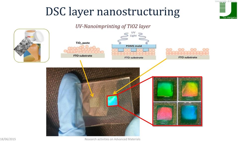
16 DSC layer nanostructuring UV-Nanoimprinting of TiO2 layer


17 DSC layer nanostructuring UV-Nanoimprinting of TiO2 layer

18 Morphological characterization ACK Dr. E. Placidi, Dr. I. Cacciotti

19 Optical characterization Integrating sphere system measurements 50 2,0 Transmittance (%) (a) Reflectance (%) 1,5 1,0 (b) Legend: Standard cell Nanostructured 0, Wavelength (nm) Wavelength (nm) Lower transmittance and lower reflectance means enhanced absorption Collaboration
 Lower transmittance and lower reflectance means enhanced absorption")
 43828-43833.")
20 Photovoltaic characterization Legend: Standard cell Nanostructured +15% Density of current (J SC ) +6% Voltage (V OC ) +32% of IPCE L. D Amico, D. Colonna, R. De Angelis, M. Casalboni, F. De Matteis, A. Di Carlo, P. Prosposito. RSC Advances 4 (2014) Collaboration
 43828-43833.")


21 Recent Challange: Large area replication 0,25 cm 2 greater by a factor of 10! 2,5 cm 2 E. Calabrò. Tesi Magistrale in Scienze e Tecnologie dei Materiali. «Ottimizzazione di Perovskite Solar cell e DSC mediante reticoli di Bragg di larga area Collaboration
22 Recent Challange: 2D Structures & Replication 0,06 Reflectance (s-pol, i =20 ) 0,05 0,04 0,03 0, Wavelength (nm) without coating with coating Collaboration
23 Thank you for attention!
24 Pubblications & other activieties [1] R. De Angelis, L. D Amico, M. Casalboni, F. Hatami, W.T. Masselink, P. Prosposito, Surface InP Quantum Dots: Effect of Morphology on the Photoluminescence Sensitivity ; Procedia Engineering, 26th European Conference on Solid-State Transducers, EUROSENSORS [2] R. De Angelis, L. D Amico, M. Casalboni, F. Hatami, W.T. Masselink, P. Prosposito, Photoluminescence sensitivity to methanol vapours of surface InP quantum dot: Effect of dot size and coverage ; Sensors and Actuators B: Chemical, February [3] R. De Angelis, M. Casalboni, I. Colantoni, L. D Amico, F. De Matteis, F. Hatami, W.T. Masselink, P. Prosposito. Luminescence sensitivity investigations on epitaxial surface InP quantum dots ; Journal of Sensor Technology, [4] R. De Angelis, Ilaria Fratoddi, F. De Matteis, P. Prosposito, I. Cacciotti, L. D'Amico, F. Nanni, A.Yadav, M. Casalboni, M. V Russo. From nanospheres to microribbons: self-assembled Eosin Y doped PMMA nanoparticles as photonic crystals ; Journal of Colloid Interface Sci.,2013. [5] R. De Angelis, M. Casalboni, L. D Amico, F. De Matteis, F. Hatami, W. T. Masselink, P. Prosposito. Vapour sensitivity of InP Surface Quantum Dots, Accepted for publication in Key Engineering Materials, [6] L. D Amico, D. Colonna, R. De Angelis, M. Casalboni, F. De Matteis, A. Di Carlo, P. Prosposito. Bragg grating Nanostructuring of TiO 2 layer in dye sensitized solar cells: an efficien method to enhance light harvesting. RSC Advances, Symposium: Innovative solar cells for renewable and sustainable energy production, Milan 18 December Bragg grating nanostructuring for light harvesting in Dye Sensitized Solar Cells (talk) Tutoring Activity Physics 1 excercises
Light management for photovoltaics using surface nanostructures
 Light management for photovoltaics using surface nanostructures Roberta De Angelis Department of Industrial Engineering and INSTM, University of Rome Tor Vergata New Materials For Optoelectronics webnemo.uniroma2.it
Simple and scalable fabrication approaches of Nanophotonic structures for PV
 Simple and scalable fabrication approaches of Nanophotonic structures for PV Fabien Sorin Surface du Verre et Interfaces (SVI), UMR 125 CNRS/Saint-Gobain, 39, Quai Lucien Lefranc, 93303 Aubervilliers,
Light management for photovoltaics. Ando Kuypers, TNO Program manager Solar
 Light management for photovoltaics Ando Kuypers, TNO Program manager Solar Global energy consumption: 500 ExaJoule/Year Solar irradiation on earth sphere: 5.000.000 ExaJoule/year 2 Capturing 0,01% covers
Basic principles and mechanisms of NSOM; Different scanning modes and systems of NSOM; General applications and advantages of NSOM.
 Lecture 16: Near-field Scanning Optical Microscopy (NSOM) Background of NSOM; Basic principles and mechanisms of NSOM; Basic components of a NSOM; Different scanning modes and systems of NSOM; General
Ultrahigh-efficiency solar cells based on nanophotonic design
 Ultrahigh-efficiency solar cells based on nanophotonic design Albert Polman Piero Spinelli Jorik van de Groep Claire van Lare Bonna Newman Erik Garnett Marc Verschuuren Ruud Schropp Wim Sinke Center for
Focused Ion beam nanopatterning: potential application in photovoltaics
 Focused Ion beam nanopatterning: potential application in photovoltaics Research Infrastructure: Location: FIB-Focused Ion Beam ENEA Portici (Italy) Date March, 26 2013 Speakers: Vera La Ferrara, ENEA
Spectral Characterisation of Photovoltaic Devices Technical Note
 Spectral Characterisation of Photovoltaic Devices Technical Note Introduction to PV This technical note provides an overview of the photovoltaic (PV) devices of today, and the spectral characterisation
Excimer Laser Technology
 D. Basting G. Marowsky (Eds.) Excimer Laser Technology With 257 Figures ^y Springer Contents 1 Introduction 1 1.1 Introductory Remarks 1 1.1.1 The Unique Microstructuring Capabilities of Excimer Lasers
Porous silicon based optical multilayers
 Porous silicon based optical multilayers PhD thesis János Volk Supervisor: Dr. István Bársony MTA Research Institute for Technical Physics and Materials Sciences Budapest 2005 Premises Due to the discovery
Organic semiconductors
 Plastic (Organic) Solar Cells: Accomplishments, Challenges, and Strategies Sumit Chaudhary Assistant Professor Department of Electrical and Computer Engineering Materials Science and Engineering Iowa State
Laboratory #3 Guide: Optical and Electrical Properties of Transparent Conductors -- September 23, 2014
 Laboratory #3 Guide: Optical and Electrical Properties of Transparent Conductors -- September 23, 2014 Introduction Following our previous lab exercises, you now have the skills and understanding to control
The study of structural and optical properties of TiO 2 :Tb thin films
 Optica Applicata, Vol. XXXVII, No. 4, 2007 The study of structural and optical properties of TiO 2 :Tb thin films AGNIESZKA BORKOWSKA, JAROSLAW DOMARADZKI, DANUTA KACZMAREK, DAMIAN WOJCIESZAK Faculty of
OPTIMIZING OF THERMAL EVAPORATION PROCESS COMPARED TO MAGNETRON SPUTTERING FOR FABRICATION OF TITANIA QUANTUM DOTS
 OPTIMIZING OF THERMAL EVAPORATION PROCESS COMPARED TO MAGNETRON SPUTTERING FOR FABRICATION OF TITANIA QUANTUM DOTS Vojtěch SVATOŠ 1, Jana DRBOHLAVOVÁ 1, Marian MÁRIK 1, Jan PEKÁREK 1, Jana CHOMOCKÁ 1,
JOURNAL INTEGRATED CIRCUITS AND SYSTEMS, VOL 1, NO. 3, JULY 2006. 39
 JOURNAL INTEGRATED CIRCUITS AND SYSTEMS, VOL 1, NO. 3, JULY 2006. 39 Self-Assembled Polystyrene Micro-Spheres Applied for Photonic Crystals and Templates Fabrication Daniel S. Raimundo 1, Francisco J.
TECNOTTICA CONSONNI SRL CERTIFIED QUALITY MANAGEMENT SYSTEM COMPANY BY DNV UNI EN ISO 9001:2008
 TECNOTTICA CONSONNI SRL CERTIFIED QUALITY MANAGEMENT SYSTEM COMPANY BY DNV UNI EN ISO 9001:2008 OUR COMPANY Tecnottica Consonni is an optical manufacturing company specialized since 1957 in the manufacture
NANO SILICON DOTS EMBEDDED SIO 2 /SIO 2 MULTILAYERS FOR PV HIGH EFFICIENCY APPLICATION
 NANO SILICON DOTS EMBEDDED SIO 2 /SIO 2 MULTILAYERS FOR PV HIGH EFFICIENCY APPLICATION Olivier Palais, Damien Barakel, David Maestre, Fabrice Gourbilleau and Marcel Pasquinelli 1 Outline Photovoltaic today
Solar Photovoltaic (PV) Cells
 Cells") Solar Photovoltaic (PV) Cells A supplement topic to: Mi ti l S Micro-optical Sensors - A MEMS for electric power generation Science of Silicon PV Cells Scientific base for solar PV electric power generation
Solar Photovoltaic (PV) Cells A supplement topic to: Mi ti l S Micro-optical Sensors - A MEMS for electric power generation Science of Silicon PV Cells Scientific base for solar PV electric power generation
Project 2B Building a Solar Cell (2): Solar Cell Performance
: Solar Cell Performance") April. 15, 2010 Due April. 29, 2010 Project 2B Building a Solar Cell (2): Solar Cell Performance Objective: In this project we are going to experimentally measure the I-V characteristics, energy conversion
April. 15, 2010 Due April. 29, 2010 Project 2B Building a Solar Cell (2): Solar Cell Performance Objective: In this project we are going to experimentally measure the I-V characteristics, energy conversion
Technology White Papers nr. 13 Paul Holister Cristina Román Vas Tim Harper
 QUANTUM DOTS Technology White Papers nr. 13 Paul Holister Cristina Román Vas Tim Harper QUANTUM DOTS Technology White Papers nr. 13 Release Date: Published by Científica Científica, Ltd. www.cientifica.com
The Physics of Energy sources Renewable sources of energy. Solar Energy
 The Physics of Energy sources Renewable sources of energy Solar Energy B. Maffei [email protected] Renewable sources 1 Solar power! There are basically two ways of using directly the radiative
Graphene a material for the future
 Graphene a material for the future by Olav Thorsen What is graphene? What is graphene? Simply put, it is a thin layer of pure carbon What is graphene? Simply put, it is a thin layer of pure carbon It has
Chemical Synthesis. Overview. Chemical Synthesis of Nanocrystals. Self-Assembly of Nanocrystals. Example: Cu 146 Se 73 (PPh 3 ) 30
 30") Chemical Synthesis Spontaneous organization of molecules into stable, structurally well-defined aggregates at the nanometer length scale. Overview The 1-100 nm nanoscale length is in between traditional
Chemical Synthesis Spontaneous organization of molecules into stable, structurally well-defined aggregates at the nanometer length scale. Overview The 1-100 nm nanoscale length is in between traditional
Conductivity of silicon can be changed several orders of magnitude by introducing impurity atoms in silicon crystal lattice.
 CMOS Processing Technology Silicon: a semiconductor with resistance between that of conductor and an insulator. Conductivity of silicon can be changed several orders of magnitude by introducing impurity
Neuere Entwicklungen zur Herstellung optischer Schichten durch reaktive. Wolfgang Hentsch, Dr. Reinhard Fendler. FHR Anlagenbau GmbH
 Neuere Entwicklungen zur Herstellung optischer Schichten durch reaktive Sputtertechnologien Wolfgang Hentsch, Dr. Reinhard Fendler FHR Anlagenbau GmbH Germany Contents: 1. FHR Anlagenbau GmbH in Brief
Recent developments in high bandwidth optical interconnects. Brian Corbett. www.tyndall.ie
 Recent developments in high bandwidth optical interconnects Brian Corbett Outline Introduction to photonics for interconnections Polymeric waveguides and the Firefly project Silicon on insulator (SOI)
Surface plasmon nanophotonics: optics below the diffraction limit
 Surface plasmon nanophotonics: optics below the diffraction limit Albert Polman Center for nanophotonics FOM-Institute AMOLF, Amsterdam Jeroen Kalkman Hans Mertens Joan Penninkhof Rene de Waele Teun van
Robert G. Hunsperger. Integrated Optics. Theory and Technology. Fourth Edition. With 195 Figures and 17 Tables. Springer
 Robert G. Hunsperger Integrated Optics Theory and Technology Fourth Edition With 195 Figures and 17 Tables Springer Contents 1. Introduction 1 1.1 Advantages of Integrated Optics 2 1.1.1 Comparison of
Patrick F. Murphy, Ph.D., P.E., CFEI Senior Managing Engineer
 Senior Managing Engineer Professional Profile Dr. Murphy s background is in electrical and electronic engineering, including electronic and optoelectronic devices, circuits, and networks. His project experience
Pulsed laser deposition of organic materials
 Pulsed laser deposition of organic materials PhD theses Gabriella Kecskeméti Department of Optics and Quantum Electronics University of Szeged Supervisor: Dr. Béla Hopp senior research fellow Department
Production of Solar Energy Using Nanosemiconductors
 Production of Solar Energy Using Nanosemiconductors 1 Kiruthika S, 2 Dinesh Kumar M, 3 Surendar.A 1, 2 II year, KSR College of Engineering, Tiruchengode, Tamilnadu, India 3 Assistant Professor, KSR College
Nanoscience Course Descriptions
 Nanoscience Course Descriptions NANO*1000 Introduction to Nanoscience This course introduces students to the emerging field of nanoscience. Its representation in popular culture and journalism will be
Applied Physics of solar energy conversion
 Applied Physics of solar energy conversion Conventional solar cells, and how lazy thinking can slow you down Some new ideas *************************************************************** Our work on semiconductor
GREEN NANOTECHNOLOGY. Geoffrey. Energy in the Built Environment. Solutions for Sustainability and. B. Smith Claes G. Granqvist.
 GREEN NANOTECHNOLOGY Solutions for Sustainability and Energy in the Built Environment Geoffrey B. Smith Claes G. Granqvist CRC Press Taylor & Francis Group Boca Raton London NewYork CRC Press is an imprint
Over the last 50 years, commercial silicon photovoltaics
 Light Trapping in Silicon Nanowire Solar Cells Erik Garnett and Peidong Yang* Department of Chemistry, University of California, Berkeley, California 94720 pubs.acs.org/nanolett ABSTRACT Thin-film structures
Back to Basics Fundamentals of Polymer Analysis
 Back to Basics Fundamentals of Polymer Analysis Using Infrared & Raman Spectroscopy Molecular Spectroscopy in the Polymer Manufacturing Process Process NIR NIR Production Receiving Shipping QC R&D Routine
UNIT I: INTRFERENCE & DIFFRACTION Div. B Div. D Div. F INTRFERENCE
 107002: EngineeringPhysics Teaching Scheme: Lectures: 4 Hrs/week Practicals-2 Hrs./week T.W.-25 marks Examination Scheme: Paper-50 marks (2 hrs) Online -50marks Prerequisite: Basics till 12 th Standard
Materials for Organic Electronic. Jeremy Burroughes FRS FREng
 Materials for Organic Electronic Applications Jeremy Burroughes FRS FREng Introduction Organic Thin Film Transistors Organic Solar Cells and Photodiodes All Printed OLED Summary 4k2k 56 Displays Panasonic
SOLAR ELECTRICITY: PROBLEM, CONSTRAINTS AND SOLUTIONS
 SOLAR ELECTRICITY: PROBLEM, CONSTRAINTS AND SOLUTIONS The United States generates over 4,110 TWh of electricity each year, costing $400 billion and emitting 2.5 billion metric tons of carbon dioxide (Yildiz,
Micro-Power Generation
 Micro-Power Generation Elizabeth K. Reilly February 21, 2007 TAC-meeting 1 Energy Scavenging for Wireless Sensors Enabling Wireless Sensor Networks: Ambient energy source Piezoelectric transducer technology
Why silicon MEMS? MEMS@KTH. Silicon is a strong material... Photolithography. Micromachining. Dicing and packaging
 Why silicon MEMS? MEMS@KTH Small Identical Large volumes (low cost per unit) School of Electrical Engineering Royal Institute of Technology Silicon is a strong material... Photolithography 10 µm thick
Rapid Prototyping and Development of Microfluidic and BioMEMS Devices
 Rapid Prototyping and Development of Microfluidic and BioMEMS Devices J. Sasserath and D. Fries Intelligent Micro Patterning System Solutions, LLC St. Petersburg, Florida (T) 727-522-0334 (F) 727-522-3896
A Promising Energy Source for Portable MEMS Devices
 A Promising Energy Source for Portable MEMS Devices S.K. Chou *, Yang Wenming, Li Zhiwang and Li Jun Department of Mechanical Engineering, National University of Singapore, 9 Engineering Drive, Singapore
Experiment #5: Qualitative Absorption Spectroscopy
 Experiment #5: Qualitative Absorption Spectroscopy One of the most important areas in the field of analytical chemistry is that of spectroscopy. In general terms, spectroscopy deals with the interactions
Hard Condensed Matter WZI
 Hard Condensed Matter WZI Tom Gregorkiewicz University of Amsterdam VU-LaserLab Dec 10, 2015 Hard Condensed Matter Cluster Quantum Matter Optoelectronic Materials Quantum Matter Amsterdam Mark Golden Anne
We know how to write nanometer. extreme lithography. extreme lithography. xlith Gesellschaft für Hochauflösende Lithografie Support & Consulting mbh
 extreme lithography extreme lithography xlith Gesellschaft für Hochauflösende Lithografie Support & Consulting mbh Wilhelm-Runge-Str. 11 89081 Ulm Germany phone +49 731 505 59 00 fax +49 731 505 59 05
5. Scanning Near-Field Optical Microscopy 5.1. Resolution of conventional optical microscopy
 5. Scanning Near-Field Optical Microscopy 5.1. Resolution of conventional optical microscopy Resolution of optical microscope is limited by diffraction. Light going through an aperture makes diffraction
2. Deposition process
 Properties of optical thin films produced by reactive low voltage ion plating (RLVIP) Antje Hallbauer Thin Film Technology Institute of Ion Physics & Applied Physics University of Innsbruck Investigations
Raman spectroscopy Lecture
 Raman spectroscopy Lecture Licentiate course in measurement science and technology Spring 2008 10.04.2008 Antti Kivioja Contents - Introduction - What is Raman spectroscopy? - The theory of Raman spectroscopy
Photonic Hydrophones based on Coated Fiber Bragg Gratings
 Photonic Hydrophones based on Coated Fiber Bragg Gratings M. Pisco, M. Moccia, M. Consales, V. Galdi, A. Cutolo, A. Cusano Optoelectronics Division, Engineering Department, University of Sannio, Benevento,
Effect of Deposition Time on ZnS Thin Films Properties by Chemical Bath Deposition (CBD) Techinique
 Techinique") World Applied Sciences Journal 19 (8): 1087-1091, 01 ISSN 1818-495 IDOSI Publications, 01 DOI: 10.589/idosi.wasj.01.19.08.591 Effect of Deposition Time on ZnS Thin Films Properties by Chemical Bath Deposition
World Applied Sciences Journal 19 (8): 1087-1091, 01 ISSN 1818-495 IDOSI Publications, 01 DOI: 10.589/idosi.wasj.01.19.08.591 Effect of Deposition Time on ZnS Thin Films Properties by Chemical Bath Deposition
Master in Condensed Matter Physics. Master académique
 Master in Condensed Matter Physics Master académique 2 " A research centered university with a personal atmosphere and multicultural flair " Students at the University of Luxembourg 3 Do it like Einstein,
RAY TRACING UNIFIED FIELD TRACING
 RAY TRACING Start to investigate the performance of your optical system using 3D ray distributions, dot diagrams of ray positions and directions, and optical path length. GEOMETRIC FIELD TRACING Switch
Optical Hyperdoping: Transforming Semiconductor Band Structure for Solar Energy Harvesting
 Optical Hyperdoping: Transforming Semiconductor Band Structure for Solar Energy Harvesting 3G Solar Technologies Multidisciplinary Workshop MRS Spring Meeting San Francisco, CA, 5 April 2010 Michael P.
Fabrication and Characterization of Nanostructured Silicon Films For Photovoltaic Applications. Kai Wang
 Fabrication and Characterization of Nanostructured Silicon Films For Photovoltaic Applications by Kai Wang A thesis submitted to the Faculty of Graduated and Postdoctoral Affairs in partial fulfillment
Types of Epitaxy. Homoepitaxy. Heteroepitaxy
 Epitaxy Epitaxial Growth Epitaxy means the growth of a single crystal film on top of a crystalline substrate. For most thin film applications (hard and soft coatings, optical coatings, protective coatings)
Characterization of surfaces by AFM topographical, mechanical and chemical properties
 Characterization of surfaces by AFM topographical, mechanical and chemical properties Jouko Peltonen Department of physical chemistry Åbo Akademi University Atomic Force Microscopy (AFM) Contact mode AFM
Acousto-optic modulator
 1 of 3 Acousto-optic modulator F An acousto-optic modulator (AOM), also called a Bragg cell, uses the acousto-optic effect to diffract and shift the frequency of light using sound waves (usually at radio-frequency).
Novel inkjettable copper ink utilizing processing temperatures under 100 degrees C without the need of inert atmosphere
 Novel inkjettable copper ink utilizing processing temperatures under 100 degrees C without the need of inert atmosphere Printed Electronics Europe April 7-8, 2009 Dresden, Germany Dr. Zvi Yaniv Applied
Outline. Self-assembled monolayer (SAM) formation and growth. Metal nanoparticles (NP) anchoring on SAM
 formation and growth. Metal nanoparticles (NP) anchoring on SAM") From functional nanostructured surfaces to innovative optical biosensors Giacomo Dacarro Dipartimento di Fisica A.Volta Dipartimento di Chimica Generale Università degli Studi di Pavia Dalla scienza dei
From functional nanostructured surfaces to innovative optical biosensors Giacomo Dacarro Dipartimento di Fisica A.Volta Dipartimento di Chimica Generale Università degli Studi di Pavia Dalla scienza dei
Near-field scanning optical microscopy (SNOM)
") Adviser: dr. Maja Remškar Institut Jožef Stefan January 2010 1 2 3 4 5 6 Fluorescence Raman and surface enhanced Raman 7 Conventional optical microscopy-limited resolution Two broad classes of techniques
Adviser: dr. Maja Remškar Institut Jožef Stefan January 2010 1 2 3 4 5 6 Fluorescence Raman and surface enhanced Raman 7 Conventional optical microscopy-limited resolution Two broad classes of techniques
Durability and Scale-Up of PerovskiteBased Mesoscopic Solar Cells
 Durability and Scale-Up of PerovskiteBased Mesoscopic Solar Cells Adriana Paracchino, Nancy Jiang, Paul Murray, Timothy Lee, Celeste Choo, Kristen Tandy, Dongchuan Fu, Francis Au, Taro Sumitomo, Hans Desilvestro,
The effect of film thickness on physical properties of fluorine-doped indium oxide thin films
 Materials Science-Poland, Vol. 22, No. 2, 2004 The effect of film thickness on physical properties of fluorine-doped indium oxide thin films S. M. ROZATI *, T. GANJ Physics Department, University of Guilan,
Nanotechnology and Its Impact on Modern Computer
 Global Journal of Researches in Engineering General Engineering Volume 12 Issue 4 Version 1.0 Year 2012 Type: Double Blind Peer Reviewed International Research Journal Publisher: Global Journals Inc. (USA)
NOVEL SOLAR CELL CONCEPTS
 NOVEL SOLAR CELL CONCEPTS Dissertation zur Erlangung des akademischen Grades des Doktors der Naturwissenschaften (Dr. rer. nat.) an der Universität Konstanz Fachbereich Physik vorgelegt von Jan Christoph
Ricerca su celle fotovoltaiche innovative
 Accordo di Programma MSE-ENEA RICERCA DI SISTEMA ELETTRICO Ricerca su celle fotovoltaiche innovative Paola Delli Veneri ENEA Una o più immagini specifiche per il progetto Energia elettrica da Fonte solare
Scanning Near-Field Optical Microscopy for Measuring Materials Properties at the Nanoscale
 Scanning Near-Field Optical Microscopy for Measuring Materials Properties at the Nanoscale Outline Background Research Design Detection of Near-Field Signal Submonolayer Chemical Sensitivity Conclusions
Low-cost Printed Electronic Nose Gas Sensors for Distributed Environmental Monitoring
 Low-cost Printed Electronic Nose Gas Sensors for Distributed Environmental Monitoring Vivek Subramanian Department of Electrical Engineering and Computer Sciences University of California, Berkeley RD83089901
Materials and Technologies for Renewable Energy. ENEA R&D activities on PV. Anna De Lillo
 Italian National Agency for New Technologies, Energy and Sustainable Economic Development Materials and Technologies for Renewable Energy ENEA R&D activities on PV Anna De Lillo ENEA UTT-RINN Castel Romano,
MCQ - ENERGY and CLIMATE
 1 MCQ - ENERGY and CLIMATE 1. The volume of a given mass of water at a temperature of T 1 is V 1. The volume increases to V 2 at temperature T 2. The coefficient of volume expansion of water may be calculated
OLED display. Ying Cao
 OLED display Ying Cao Outline OLED basics OLED display A novel method of fabrication of flexible OLED display Potentials of OLED Suitable for thin, lightweight, printable displays Broad color range Good
Scientific Exchange Program
 Scientific Exchange Program Electrical characterization of photon detectors based on acoustic charge transport Dr. Paulo Santos, Paul Drude Institute, Berlin,Germany Dr. Pablo Diniz Batista, Brazilian
Arizona Institute for Renewable Energy & the Solar Power Laboratories
 Arizona Institute for Renewable Energy & the Solar Power Laboratories International Photovoltaic Reliability Workshop July 29-31, Tempe AZ Christiana Honsberg, Stephen Goodnick, Stuart Bowden Arizona State
Integrated Photonic. Electronic. Optics. Optoelettronics. Integrated Photonic - G. Breglio L1. Quantum Mechanics Materials Science Nano/Bio-photonic
 Integrated Photonic Quantum Mechanics Materials Science Nano/Bio-photonic Optoelettronics Optics Electronic Applications of Optoelectronic Systems Solar cells OLED display LED Laser diodes Flexible OLED
Esnek Güneş Pilleri ve Fotovoltaik Tekstiller
 Esnek Güneş Pilleri ve Fotovoltaik Tekstiller (Flexible Solar Cells and Photovoltaic Textiles) AYŞE (ÇELİK) BEDELOĞLU Yrd. Doç. Dr. Lif ve Polimer Mühendisliği Bursa Teknik Üniversitesi Work experience
2 Absorbing Solar Energy
 2 Absorbing Solar Energy 2.1 Air Mass and the Solar Spectrum Now that we have introduced the solar cell, it is time to introduce the source of the energy the sun. The sun has many properties that could
Graduate Student Presentations
 Graduate Student Presentations Dang, Huong Chip packaging March 27 Call, Nathan Thin film transistors/ liquid crystal displays April 4 Feldman, Ari Optical computing April 11 Guerassio, Ian Self-assembly
CREOL, College of Optics & Photonics, University of Central Florida
 OSE6650 - Optical Properties of Nanostructured Materials Optical Properties of Nanostructured Materials Fall 2013 Class 3 slide 1 Challenge: excite and detect the near field Thus far: Nanostructured materials
Deposition of Conducting Oxide Thin Films as Anode for Solar Cell Device
 British Journal of Applied Science & Technology 4(5): 739-748, 2014 SCIENCEDOMAIN international www.sciencedomain.org Deposition of Conducting Oxide Thin Films as Anode for Solar Cell Device N. Mustapha
Staff: 1277 including students and student assistants Annual Budget: 86,1 million euros, including investments. (December 2014)
") Fraunhofer Institute for Solar Energy Systems ISE A short overview The Institute The Fraunhofer Institute for Solar Energy Systems ISE is committed to promoting sustainable, economic, safe and socially
Fraunhofer Institute for Solar Energy Systems ISE A short overview The Institute The Fraunhofer Institute for Solar Energy Systems ISE is committed to promoting sustainable, economic, safe and socially
Spectral Measurement Solutions for Industry and Research
 Spectral Measurement Solutions for Industry and Research Hamamatsu Photonics offers a comprehensive range of products for spectroscopic applications, covering the, Visible and Infrared regions for Industrial,
Advanced Laser Microfabrication in High Volume Manufacturing
 Advanced Laser Microfabrication in High Volume Manufacturing IPG Photonics Microsystems Division 220 Hackett Hill Road, Manchester NH, 03102USA E-mail: [email protected] There is increased interest
How To Increase Areal Density For A Year
 R. Fontana¹, G. Decad¹, S. Hetzler² ¹IBM Systems Technology Group, ²IBM Research Division 20 September 2012 Technology Roadmap Comparisons for TAPE, HDD, and NAND Flash: Implications for Data Storage Applications
Laserwelding of plastics Ir. Luc Janssen 2008
 3D Laserwelding page 1 of 12 Laserwelding of plastics Ir. Luc Janssen 2008 1 Laserwelding - How it works Laserwelding is a very versatile process and is suitable for both small series and massproduction.
Le nanotecnologie: dal Laboratorio al Mercato. Fabrizio Pirri Politecnico di Torino Istituto Italiano di Tecnologia
 Le nanotecnologie: dal Laboratorio al Mercato Fabrizio Pirri Politecnico di Torino Istituto Italiano di Tecnologia Materials & Processes for micro nanotechnologies Laboratory http://www.polito.it/micronanotech
Celle solari di terza generazione (a fotosintesi )
") Celle solari di terza generazione (a fotosintesi ) Esempi: photoelectrochemical cells, polymer solar cells (quarta generazione), nanocrystal solar cells (a quantum dots), Dye-sensitized solar cells Celle
Celle solari di terza generazione (a fotosintesi ) Esempi: photoelectrochemical cells, polymer solar cells (quarta generazione), nanocrystal solar cells (a quantum dots), Dye-sensitized solar cells Celle
Problem Set 6 UV-Vis Absorption Spectroscopy. 13-1. Express the following absorbances in terms of percent transmittance:
 Problem Set 6 UV-Vis Absorption Spectroscopy 13-1. Express the following absorbances in terms of percent transmittance: a 0.051 b 0.918 c 0.379 d 0.261 e 0.485 f 0.072 A = log P o /P = log1/t = - log T
Micro Power Generators. Sung Park Kelvin Yuk ECS 203
 Micro Power Generators Sung Park Kelvin Yuk ECS 203 Overview Why Micro Power Generators are becoming important Types of Micro Power Generators Power Generators Reviewed Ambient Vibrational energy Radiant
Lecture 15 - application of solid state materials solar cells and photovoltaics. Copying Nature... Anoxygenic photosynthesis in purple bacteria
 Lecture 15 - application of solid state materials solar cells and photovoltaics. Copying Nature... Anoxygenic photosynthesis in purple bacteria Simple example, but still complicated... Photosynthesis is
Emerging new non conventional tools
 Emerging new non conventional tools Near field lithography Near field lithography Near field lithography through local electrochemistry example of gold a) Surface water condensation b) Monolayer of oxidized
Grad Student Presentation Topics PHGN/CHEN/MLGN 435/535: Interdisciplinary Silicon Processing Laboratory
 Grad Student Presentation Topics 1. Baranowski, Lauryn L. AFM nano-oxidation lithography 2. Braid, Jennifer L. Extreme UV lithography 3. Garlick, Jonathan P. 4. Lochner, Robert E. 5. Martinez, Aaron D.
Development of the Extreme Ultraviolet Spectrometer: EXCEED
 Development of the Extreme Ultraviolet Spectrometer: EXCEED Go Murakami*, Kazuo Yoshioka, Atsushi Yamazaki, Tomoki Kimura Institute of Space and Astronautical Science, Japan Aerospace Exploration Agency
Luminescence and Optical Properties of Tm 3+ :TeO 2 - ZnO-TiO 2 Glasses for Fiber Optic Applications
 Luminescence and Optical Properties of Tm + :TeO - ZnO-TiO Glasses for Fiber Optic Applications İdris Kabalcı 1, Turgay Tay Tuğba Duran, Mustafa Özdemir, Gönül Özen 4 1 Department of Physics Education,,
Supporting Information. Rapid Prototyping of Microchannels with Surface Patterns for Fabrication of Polymer Fibers
 Electronic Supplementary Material (ESI) for RSC Advances. This journal is The Royal Society of Chemistry 2015 Supporting Information Rapid Prototyping of Microchannels with Surface Patterns for Fabrication
BROADBAND PHOTOCURRENT ENHANCEMENT IN LONGWAVE INFRARED QUANTUM DOT PHOTODETECTORS BY SUB-WAVELENGTH SURFACE GRATINGS
 Optics and Photonics Letters Vol. 6, No. 1 (2013) 1350002 (6 pages) c World Scientific Publishing Company DOI: 10.1142/S1793528813500020 BROADBAND PHOTOCURRENT ENHANCEMENT IN LONGWAVE INFRARED QUANTUM