Ver 1.2 4~32G High Capacity microsd Card. Features. Description. Placement. Pin Definition. Transcend Information Inc. 1
|
|
|
- Jennifer Osborne
- 9 years ago
- Views:
Transcription
1 Description Transcend High Capacity microsd Card series are specifically designed to meet the High Capacity, High Definition Audio and Video requirement for the latest Digital Cameras, DV Recorders, Mobile Phones, etc. The new defined Speed Class enables the host to support AV applications to perform real time recording to the microsd memory card. Placement Features RoHS compliant product. Operating Voltage: 2.7 ~ 3.6V Operating Temperature: -25 ~ 85 C Durability: 10,000 insertion/removal cycles Compatible with SD Specification Ver. 3.0 Comply with SD File System Specification Ver. 3.0 Mechanical Write Protection Switch with microsd adapter Supports Speed Class Specification Class 10 Supports Copy Protection for Recorded Media (CPRM) for SD-Audio Form Factor: 11mm x 15mm x 1mm Front Pin Definition Back Pin No. 1 SD Mode SPI Mode Name Type Description Name Type Description DAT2 I/O/PP Data Line [Bit2] RSV Reserved 2 CD/DAT3 I/O/PP Card Detect / Data Line [Bit3] CS I Chip Select 3 CMD PP Command / Response DI I Data In 4 V DD S Supply voltage V DD S Supply voltage 5 CLK I Clock SCLK I Clock 6 V SS S Supply voltage ground V SS S Supply voltage ground 7 DAT0 I/O/PP Data Line [Bit0] DO O/PP Data out 8 DAT1 I/O/PP Data Line [Bit1] RSV Reserved S: Power Supply; I:Input; O:Output; PP:Push-Pull Transcend Information Inc. 1

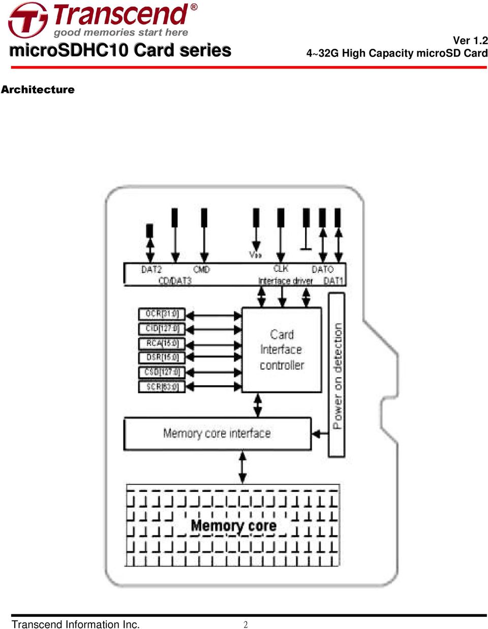
2 Architecture Transcend Information Inc. 2
3 Bus Operating Conditions General Parameter Symbol Min. Max. Unit Remark Peak voltage on all lines -0.3 V DD +0.3 V All Inputs Input Leakage Current µa All Outputs Output Leakage Current µa Power Supply Voltage Parameter Symbol Min. Max. Unit Remark Supply voltage V DD V Output High Voltage V OH 0.75* V DD V I OH =-100uA@V DD Min. Output Low Voltage V OL 0.125* V DD V I OL =100uA@V DD Min. Input High Voltage V IH 0.625* V DD V DD +0.3 V Input Low Voltage V IL V SS * V DD V Power up time 250 ms From 0v to V DD Min. Current Consumption The current consumption is measured by averaging over 1 second. Before first command: Maximum 15 ma During initialization: Maximum 100 ma Operation in Default Mode: Maximum 100 ma Operation in High Speed Mode: Maximum 200 ma Operation with other functions: Maximum 500 ma. Bus Signal Line Load The total capacitance C L the CLK line of the SD Memory Card bus is the sum of the bus master capacitance C HOST, the bus capacitance C BUS itself and the capacitance C CARD of each card connected to this line: C L = C HOST + C BUS + Ν*C CARD Where N is the number of connected cards. Pull-up resistance Parameter Symbol Min. Max. Unit Remark R CMD R DAT kω To prevent bus floating Bus signal line capacitance C L 40 pf 1 card C HOST +C BUS shall not exceed 30 pf Transcend Information Inc. 3

4 Single card capacitance C CARD 10 pf Maximum signal line inductance 16 nh f PP 20 MHz Pull-up resistance inside card (pin1) R DAT kω May be used for card detection Note that the total capacitance of CMD and DAT lines will be consist of C HOST, C BUS and one C CARD only because they are connected separately to the SD Memory Card host. Host should consider total bus capacitance for each signal as the sum of C HOST, C BUS, and C CARD, these parameters are defined by per signal. The host can determine C HOST and C BUS so that total bus capacitance is less than the card estimated capacitance load (C L =40 pf). The SD Memory Card guarantees its bus timing when total bus capacitance is less than maximum value of C L (40 pf). Transcend Information Inc. 4
.")
5 Bus Signal Levels As the bus can be supplied with a variable supply voltage, all signal levels are related to the supply voltage. To meet the requirements of the JEDEC specification JESD8-1A and JESD8-7, the card input and output voltages shall be within the following specified ranges for any V DD of the allowed voltage range: Parameter Symbol Min. Max. Unit Remark Output HIGH voltage V OH 0.75* V DD V I OH = -100 DD min Output LOW voltage V OL 0.125* V DD V I OL = -100 DD min Input HIGH voltage V IH 0.625* V DD V DD V Input LOW voltage V IL V SS * V DD V Transcend Information Inc. 5

6 Bus Timing Parameter Symbol Min Max. Unit Remark Clock CLK (All values are referred to min (V IH ) and max (V IL ) Clock frequency Data Transfer Mode f PP 0 25 MHz C CARD 10 pf, (1 card) Clock frequency Identification Mode f OD 0 (1) / KHz C CARD 10 pf, (1 card) Clock low time t WL 10 ns C CARD 10 pf, (1 card) Clock high time t WH 10 ns C CARD 10 pf, (1 card) Clock rise time t TLH 10 ns C CARD 10 pf, (1 card) Clock fall time t THL 10 ns C CARD 10 pf, (1 card) Inputs CMD, DAT (referenced to CLK) Input set-up time t ISU 5 ns C CARD 10 pf, (1 card) Input hold time t IH 5 ns C CARD 10 pf, (1 card) Outputs CMD, DAT (referenced to CLK) Output Delay time during Data Transfer Mode t ODLY 0 14 ns C L 40 pf, (1 card) Output Delay time during Identification Mode t ODLY 0 50 ns C L 40 pf, (1 card) (1) 0 Hz means to stop the clock. The given minimum frequency range is for cases were continues clock is required Transcend Information Inc. 6
 Inputs CMD, DAT (referenced to CLK) Input set-up time t ISU 5 ns C CARD 10 pf, (1 card) Input hold time t IH 5 ns C CARD 10 pf, (1 card) Outputs CMD, DAT")
7 Bus Timing (High Speed Mode) Parameter Symbol Min Max. Unit Remark Clock CLK (All values are referred to min (V IH ) and max (V IL ) Clock frequency Data Transfer Mode f PP 0 50 MHz C CARD 10 pf, (1 card) Clock low time t WL 7 ns C CARD 10 pf, (1 card) Clock high time t WH 7 ns C CARD 10 pf, (1 card) Clock rise time t TLH 3 ns C CARD 10 pf, (1 card) Clock fall time t THL 3 ns C CARD 10 pf, (1 card) Inputs CMD, DAT (referenced to CLK) Input set-up time t ISU 6 ns C CARD 10 pf, (1 card) Input hold time t IH 2 ns C CARD 10 pf, (1 card) Outputs CMD, DAT (referenced to CLK) Output Delay time during Data Transfer Mode t ODLY 14 ns C L 40 pf, (1 card) Output Hold time t OH 2.5 ns C L 40 pf, (1 card) Total System capacitance for each line 1 C L 40 pf (1 card) 1) In order to satisfy severe timing, host shall drive only one card. Transcend Information Inc. 7
 Input hold time t IH 2 ns C CARD 10 pf, (1 card) Outputs CMD, DAT (referenced to CLK) Output Delay time during Data Transfer Mode t ODLY 14 ns C L 40 pf, (1")
8 Reliability and Durability Temperature Operation: -25 C / 85 C Storage: -40 C (168h) / 85 C (500h) Junction temperature: max. 95 C Moisture and corrosion Operation: 25 C / 95% rel. humidity Storage: 40 C / 93% rel. hum./500h Salt Water Spray: 3% NaCl/35C; 24h acc. MIL STD Method 1009 Durability mating cycles; Bending 10N Torque 0.15N.m or +/-2.5 deg Drop test 1.5m free fall Visual inspection No warp page; no mold skin; complete form; no cavities surface smoothness <= -0.1 Shape and form mm/cm² within contour; no cracks; no pollution (fat, oil dust, etc.) Transcend Information Inc. 8

9 Register Information Within the card interface six registers are defined: OCR, CID, CSD, RCA, DSR and SCR. These can be accessed only by corresponding commands. The OCR, CID, CSD and SCR registers carry the card/content specific information, while the RCA and DSR registers are configuration registers storing actual configuration parameters. 1. OCR register The 32-bit operation conditions register stores the VDD voltage profile of the card. Additionally, this register includes status information bits. One status bit is set if the card power up procedure has been finished. This register includes another status bit indicating the card capacity status after set power up status bit. The OCR register shall be implemented by the cards. The 32-bit operation conditions register stores the VDD voltage profile of the card. Bit 7 of OCR is newly defined for Dual Voltage Card and set to 0 in default. If a Dual Voltage Card does not receive CMD8, OCR bit 7 in the response indicates 0, and the Dual Voltage Card which received CMD8, sets this bit to 1. Additionally, this register includes 2 more status information bits. Bit 31 - Card power up status bit, this status bit is set if the card power up procedure has been finished. Bit 30 - Card capacity status bit, this status bit is set to 1 if card is High Capacity SD Memory Card. 0 indicates that the card is Standard Capacity SD Memory Card. The Card Capacity status bit is valid after the card power up procedure is completed and the card power up status bit is set to 1. The Host shall read this status bit to identify a Standard or High Capacity SD Memory Card. The OCR register shall be implemented by the cards. Transcend Information Inc. 9

10 OCR Register Definition 1) This bit is valid only when the card power up status bit is set. 2) This bit is set to LOW if the card has not finished the power up routine. A voltage range is not supported if the corresponding bit value is set to LOW. As long as the card is busy, the corresponding bit (31) is set to LOW. 2. CID Register The Card IDentification (CID) register is 128 bits wide. It contains the card identification information used during the card identification phase. Every individual flash card shall have a unique identification number. The structure of the CID register is defined in the following paragraphs: MID An 8-bit binary number that identifies the card manufacturer. The MID number is controlled, defined, and allocated to a SD Memory Card manufacturer by the SD-3C, LLC. This procedure is established to ensure uniqueness of the CID register. OID A 2-character ASCII string that identifies the card OEM and/or the card contents (when used as a distribution media either on ROM or FLASH cards). The OID number is controlled, defined, and allocated to a SD Memory Card manufacturer by the SD-3C, LLC. This procedure is established to ensure uniqueness of the CID register. Note: SD-3C, LLC licenses companies that wish to manufacture and/or sell SD Memory Cards, including but not limited to flash memory, ROM, OTP, RAM, and SDIO Combo Cards. SD-3C, LLC is a limited liability company established by Matsushita Electric Industrial Co. Ltd., SanDisk Corporation and Toshiba Corporation. PNM The product name is a string, 5 ASCII characters long. Transcend Information Inc. 10

11 PRV The product revision is composed of two Binary Coded Decimal (BCD) digits, four bits each, representing an n.m revision number. The n is the most significant nibble and m is the least significant nibble. As an example, the PRV binary value field for product revision 6.2 will be: PSN The Serial Number is 32 bits of binary number. MDT The manufacturing date composed of two hexadecimal digits, one is 8 bit representing the year(y) and the other is four bits representing the month(m). The m field [11:8] is the month code. 1 = January. The y field [19:12] is the year code. 0 = As an example, the binary value of the Date field for production date April 2001 will be: CRC CRC7 checksum (7 bits). 3. CSD Register The following sections describe the CSD fields and the relevant data types for the High Capacity SD Memory Card. CSD Version 2.0 is applied to only the High Capacity SD Memory Card. The field name in parenthesis is set to fixed value and indicates that the host is not necessary to refer these fields. The fixed values enables host, which refers to these fields, to keep compatibility to CSD Version 1.0. The Cell Type field is coded as follows: R = readable, W(1) = writable once, W = multiple writable. Transcend Information Inc. 11
 and the other is four bits representing the month(m). The m field [11:8] is the month code.")
12 The CSD Register Fields (CSD Version 2.0) The following sections describe the CSD fields and the relevant data types. If not explicitly defined otherwise, all bit strings are interpreted as binary coded numbers starting with the left bit first. CSD_STRUCTURE Field structures of the CSD register are different depend on the Physical Specification Version and Card Capacity. The CSD_STRUCTURE field in the CSD register indicates its structure version. The following table shows the version number of the related CSD structure. Transcend Information Inc. 12

13 CSD_STRUCTURE CSD structure version Card Capacity 0 CSD Version 1.0 Standard Capacity 1 CSD Version 2.0 High Capacity and Extended Capacity 2-3 reserved CSD Register Structure TAAC This field is fixed to 0Eh, which indicates 1 ms. The host should not use TAAC, NSAC, and R2W_FACTOR to calculate timeout and should uses fixed timeout values for read and write operations. NSAC This field is fixed to 00h. NSAC should not be used to calculate time-out values. TRAN_SPEED The following table defines the maximum data transfer rate per one data line - TRAN_SPEED: Transcend Information Inc. 13

14 Note that for current SD Memory Cards that field must be always 0_0110_010b (032h) which is equal to 25MHz - the mandatory maximum operating frequency of SD Memory Card. In High-Speed mode, that field must be always 0_1011_010b (05Ah) which is equal to 50MHz. And when the timing mode returns to the default by CMD6 or CMD0 command, its value will be 032h. CCC The SD Memory Card command set is divided into subsets (command classes). The card command class register CCC defines which command classes are supported by this card. A value of 1 in a CCC bit means that the corresponding command class is supported. READ_BL_LEN This field is fixed to 9h, which indicates READ_BL_LEN=512 Byte. READ_BL_PARTIAL This field is fixed to 0, which indicates partial block read is inhibited and only unit of block access is allowed. WRITE_BLK_MISALIGN This field is fixed to 0, which indicates write access crossing physical block boundaries is always disabled in High Capacity SD Memory Card. Transcend Information Inc. 14

15 READ_BLK_MISALIGN This field is fixed to 0, which indicates read access crossing physical block boundaries is always disabled in High Capacity SD Memory Card. DSR_IMP Defines if the configurable driver stage is integrated on the card. If set, a driver stage register (DSR)must be implemented also. C_SIZE This field is expanded to 22 bits and can indicate up to 2 TBytes (It is the same as the maximum memory space specified by a 32-bit block address.) This parameter is used to calculate the user data area capacity in the SD memory card (not include the protected area). The user data area capacity is calculated from C_SIZE as follows: memory capacity = (C_SIZE+1) * 512K byte As the maximum capacity of the Physical Layer Specification Version 2.00 is 32 GB, the upper 6 bits of this field shall be set to 0. ERASE_BLK_EN This field is fixed to 1, which means the host can erase one or multiple units of 512 bytes. SECTOR_SIZE This field is fixed to 7Fh, which indicates 64 KBytes. This value does not relate to erase operation. Version 2.00 cards indicates memory boundary by AU size and this field should not be used. WP_GRP_SIZE This field is fixed to 00h. The High Capacity SD Memory Card does not support write protected groups. WP_GRP_ENABLE This field is fixed to 0. The High Capacity SD Memory Card does not support write protected groups. R2W_FACTOR This field is fixed to 2h, which indicates 4 multiples. Write timeout can be calculated by multiplying the read access time and R2W_FACTOR. However, the host should not use this factor and should use 250 ms for write timeout Transcend Information Inc. 15
 This parameter is used to calculate the user data area capacity in the SD memory card (not include the protected area).")
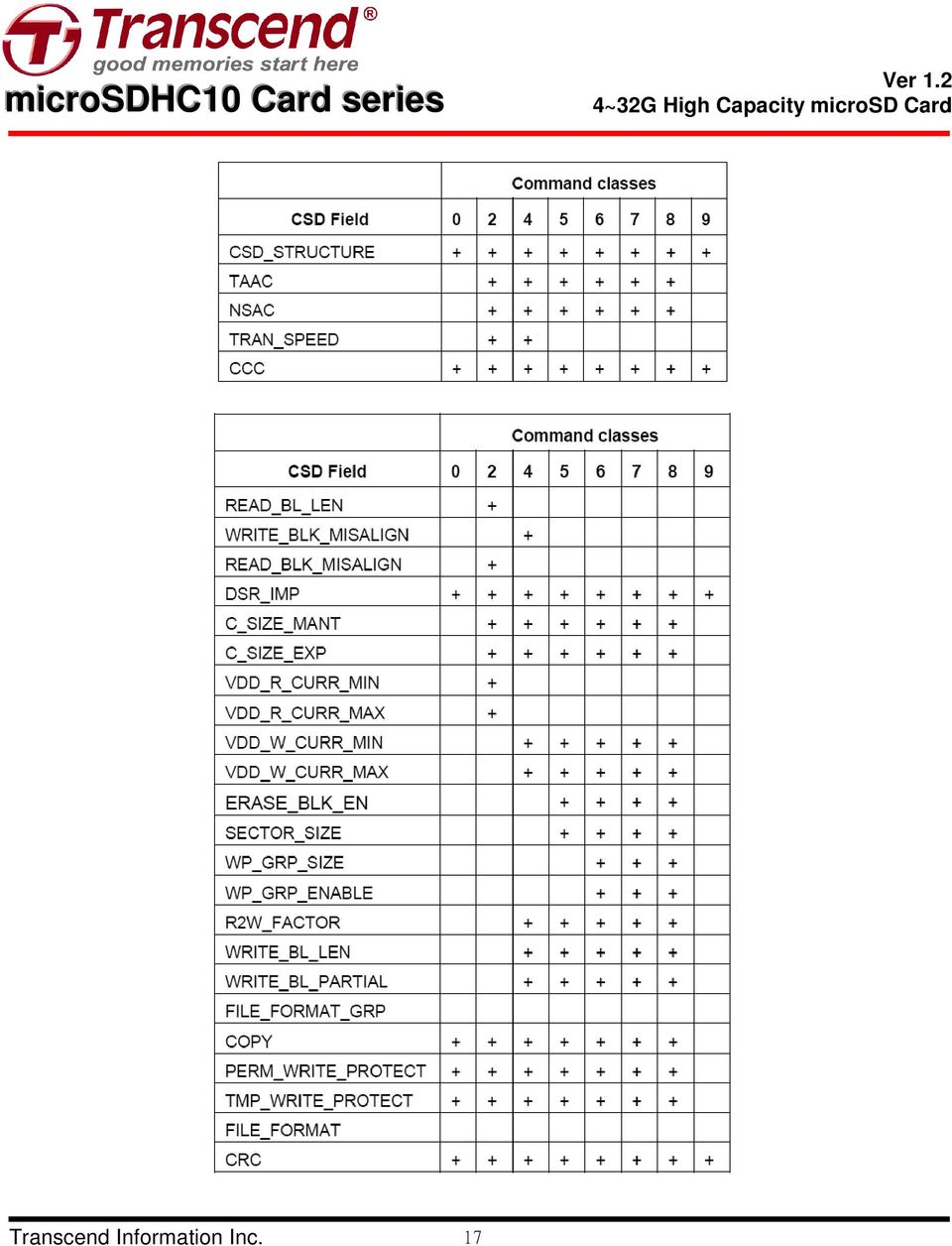
16 WRITE_BL_LEN This field is fixed to 9h, which indicates WRITE_BL_LEN=512 Byte. WRITE_BL_PARTIAL This field is fixed to 0, which indicates partial block read is inhibited and only unit of block access is allowed. FILE_FORMAT_GRP This field is set to 0. Host should not use this field. COPY Defines if the contents is original (= 0 ) or has been copied (= 1 ). The COPY bit for OTP and MTP devices, sold to end consumers, is set to 1 which identifies the card contents as a copy. The COPY bit is an one time programmable bit. PERM_WRITE_PROTECT Permanently protects the whole card content against overwriting or erasing (all write and erase commands for this card are permanently disabled). The default value is 0, i.e. not permanently write protected. TMP_WRITE_PROTECT Temporarily protects the whole card content from being overwritten or erased (all write and erase commands for this card are temporarily disabled). This bit can be set and reset. The default value is 0, i.e. not write protected. FILE_FORMAT This field is set to 0. Host should not use this field. CRC The CRC field carries the check sum for the CSD contents. The checksum has to be recalculated by the host for any CSD modification. The default corresponds to the initial CSD contents. The following table lists the correspondence between the CSD entries and the command classes. A + entry indicates that the CSD field affects the commands of the related command class. Transcend Information Inc. 16

17 Transcend Information Inc. 17
18 4. RCA Register The writable 16-bit relative card address register carries the card address that is published by the card during the card identification. This address is used for the addressed host-card communication after the card identification procedure. The default value of the RCA register is 0x0000. The value0x0000 is reserved to set all cards into the Stand-by State with CMD7. 5. DSR Register (Optional) It can be optionally used to improve the bus performance for extended operating conditions (depending on parameters like bus length, transfer rate or number of cards). The CSD register carries the information about the DSR register usage. The default value of the DSR register is 0x SCR Register In addition to the CSD register there is another configuration register that named - SD CARD Configuration Register (SCR). SCR provides information on SD Memory Card's special features that were configured into the given card. The size of SCR register is 64 bit. This register shall be set in the factory by the SD Memory Card manufacturer. The following table describes the SCR register content. Description Field Width Cell Type SCR Slic SCR Structure SCR_STRUCTURE 4 R e [63:60] SD Memory Card - Spec. Version SD_SPEC 4 R [59:56] data_status_after erases DATA_STAT_AFTER_ERASE 1 R [55:55] CPRM Security Support SD_SECURITY 3 R [54:52] DAT Bus widths supported SD_BUS_WIDTHS 4 R [51:48] Spec. Version 3.00 or higher SD_SPEC3 1 R [47] Extended Security Support EX_ SECURITY 4 R [46:43] Reserved 9 R [42:34] Command Support bits CMD_SUPPORT 14 R [33:32] reserved for manufacturer usage - 32 R [31:0] Transcend Information Inc. 18
 It can be optionally used to improve the bus performance for extended operating conditions (depending on parameters like bus length, transfer rate or number of cards).")
19 SCR_STRUCTURE Version number of the related SCR structure in the SD Memory Card Physical Layer Specification. SCR_STRUCTURE SCR structure version SD Physical Layer Specification Version 0 SCR version 1.0 Version reserved SCR Register Structure Version SD_SPEC Describes the SD Memory Card Physical Layer Specification version supported by this card. SD_SPEC Physical Layer Specification Version Number 0 Version Version 1.10 Version 2.00 or Version (Refer to SD_SPEC3) 3-15 reserved Physical Layer Specification Version SD_SPEC3 SD_SPEC SD_SPEC3 Physical Layer Specification Version Number 2 0 Version Version 3.00 The card manufacturer determines SD_SPEC value by conditions indicated below. All conditions shall be satisfied for each version. The other combination of conditions is not allowed. Essential conditions to indicate Version 1.01 Card (SD_SPEC=0 and SD_SPEC3=0) (1)The card does not support CMD6 (2)The card does not support CMD8 (3) User area capacity shall be up to 2GB Essential conditions to indicate Version 1.10 Card (SD_SPEC=1 and SD_SPEC3=0) (1) The card shall support CMD6 (2) The card does not support CMD8 (3) User area capacity shall be up to 2GB Transcend Information Inc. 19

20 Essential conditions to indicate Version 2.00 Card (SD_SPEC=2 and SD_SPEC3=0) (1) The card shall support CMD6 (2) The card shall support CMD8 (3) The card shall support CMD42 (4) User area capacity shall be up to 2GB (SDSC) or 32GB (SDHC) (5) Speed Class shall be supported (SDHC) Essential conditions to indicate Version 3.00 Card (SD_SPEC=2 and SD_SPEC3=1) (1) The card shall support CMD6 (2) The card shall support CMD8 (3) The card shall support CMD42 (4) User area capacity shall be up to 2GB (SDSC) or 32GB (SDHC) User area capacity shall be more than or equal to 32GB and up to 2TB (SDXC) (5) Speed Class shall be supported (SDHC or SDXC) A card supports any of following functions shall satisfy essential conditions of Version 3.00 Card (1) Speed Class supported under the conditions defined in Ver3.00 (2) UHS-I supported card (3) CMD23 supported card Application Notes: When checking SD_SPEC version in SCR, the host shall not forget that higher SD_SPEC version may be specified in future. It is important to keep compatibility for future version. DATA_STAT_AFTER_ERASE Defines the data status after erase, whether it is 0 or 1 (the status is card vendor dependent). Transcend Information Inc. 20
 (1) The card shall support CMD6 (2) The card shall support CMD8 (3) The card shall support CMD42 (4) User area capacity shall be up to 2GB (SDSC) or 32GB (SDHC)")
21 SD_SECURITY This field indicates CPRM Security Specification Version for each capacity card. The definition of Protected Area is different in each capacity card. SD_SECURITY CPRM Security Version 0 No Security 1 Not Used 2 SDSC Card (Security Version 1.01) 3 SDHC Card (Security Version 2.00) 4 SDXC Card (Security Version 3.xx) 5-7 Reserved The basic rule of setting this field: CPRM Security Version SDSC Card sets this field to 2 (Version 1.01) SDHC Card sets this field to 3 (Version 2.00). SDXC Card sets this field to 4 (Version 3.xx). Note that it is mandatory for a regular writable SD Memory Card to support Security Protocol. For ROM (Read Only) and OTP (One Time Programmable) types of the SD Memory Card, the security feature is optional. SD_BUS_WIDTHS Describes all the DAT bus widths that are supported by this card. SD_BUS_WIDTHS Bit 0 Bit 1 Bit 2 Bit 3 Supported Bus Widths 1 bit (DAT0) reserved 4 bit (DAT0-3) reserved SD Memory Card Supported Bus Widths Since SD Memory Card shall support at least the two bus modes 1bit or 4bit width then any SD Card shall set at least bits 0 and 2 (SD_BUS_WIDTH="0101"). Transcend Information Inc. 21
22 Mechanical Dimension Mechanical Description: Top View Transcend Information Inc. 22
23 Mechanical Description: Bottom View Transcend Information Inc. 23
24 Mechanical Description: Keep Out Area Transcend Information Inc. 24
25 microsd package: Dimensions Transcend Information Inc. 25
4~16GB High Capacity microsd Card. Description. Features. Placement. Pin Definition. Transcend Information Inc. 1
 Description Transcend High Capacity microsd Card series are specifically designed to meet the High Capacity, High Definition Audio and Video requirement for the latest Digital Cameras, DV Recorders, Mobile
microsd Memory Card Features Description Placement Pin Definition Transcend Information Inc. 1
 Description Transcend microsd card series are non-volatile, which means no external power is required to retain the information stored on it. Besides, it is also a solid-state device that without moving
Rev. 1.0. 64GB Extended Capacity Secure Digital Card. Description. Features. Placement. Pin Definition. Transcend Information Inc.
 Description Transcend secured digital extended capacity Card series are specifically designed to meet the High Capacity, High Definition Audio and Full HD Video requirement for the latest Digital Cameras,
Micro SDSC / SDHC / SDXC. Micro SD Data Sheet
 Micro SD Data Sheet Rev. 1.0 1 APR 2012 Table of Contents 1. Introduction to the micro SDSC/SDHC/SDXC............ 4 2. Micro SDSC/SDHC/SDXC Feature.............. 4 3. Product Specification.................
Industrial microsd/sdhc Memory Card
 DCC Number: Industrial microsd/sdhc Memory Card Product Specification March 2011 PRETEC/C-ONE Technology Corp. Corporate Headquarters 8F, NO5, Lane 345, Yang Guang St., Neihu, Taipei,Taiwan TEL: +886-2-2659-4380
datasheet SAMSUNG ELECTRONICS RESERVES THE RIGHT TO CHANGE PRODUCTS, INFORMATION AND SPECIFICATIONS WITHOUT NOTICE.
 Rev.1.0, May. 2011 MMBTFxxGUBCA-xMExx Samsung SD & Micro product family SDA 3.0 specification compliant-up to High Speed mode SAMSUNG ELECTRONICS RESERVES THE RIGHT TO CHANGE PRODUCTS, INFORMATION AND
SD Card Specification
 SD Card Specification Model Name : KP032S3CBS KP032S3CCS KP064S3DAS KP128S3EMS KP256S3EMS KP256S3FMS KP512S3EMS KP512S3FMS KP01GS3FMS Ver 1.1 07.08.200 1 Features Capcity:32MB/64MB/128MB/256M/512MB/1GByte
Industrial Micro SD 3.0
 RoHS Compliant Industrial Micro SD 3.0 Specifications November 3 rd, 2011 Version 1.0 Apacer Technology Inc. 4 th Fl., 75 Hsin Tai Wu Rd., Sec.1, Hsichih, New Taipei City, Taiwan 221 Tel: +886-2-2698-2888
microsdxc memory card Flash Storage Media 1. Introduction 2. Part Number 3. microsdxc memory card features Table 1: microsdxc Card Features
 microsdxc memory card Flash Storage Media 1. Introduction Industrial temperature microsdxc card is designed, manufactured and tested to withstand extreme environmental conditions. Outdoor applications
SD Specifications Part 1 Physical Layer Simplified Specification
 SD Specifications Part 1 Physical Layer Simplified Specification Version 4.10 January 22, 2013 SD Group Panasonic Corporation SanDisk Corporation Toshiba Corporation Technical Committee SD Card Association
Industrial Micro SD 3.0
 RoHS Recast Compliant Industrial Micro SD 3.0 microsdhc Product Specifications May 7, 2015 Version 1.4 Apacer Technology Inc. 1F, No.32, Zhongcheng Rd., Tucheng Dist., New Taipei City, Taiwan, R.O.C Tel:
MultiMediaCard Product Manual
 MultiMediaCard Product Manual CORPORATE HEADQUARTERS 140 Caspian Court Sunnyvale, CA 94089-1000 408-542-0500 FAX: 408-542-0503 URL: http://www.sandisk.com SanDisk Corporation general policy does not recommend
Embedded Multi-Media Card Specification (e MMC 4.5)
") Product Features: Packaged NAND flash memory with e MMC 4.5 interface Compliant with e MMC Specification Ver 4.41 & 4.5. Bus mode - High-speed e MMC protocol - Provide variable clock frequencies
Product Features: Packaged NAND flash memory with e MMC 4.5 interface Compliant with e MMC Specification Ver 4.41 & 4.5. Bus mode - High-speed e MMC protocol - Provide variable clock frequencies
SanDisk SD Card. Product Manual. Version 2.2 Document No. 80-13-00169 November 2004. SanDisk Corporation
 SanDisk SD Card Product Manual Version 2.2 Document No. 80-13-00169 November 2004 SanDisk Corporation Corporate Headquarters 140 Caspian Court Sunnyvale, CA 94089 Phone (408) 542-0500 Fax (408) 542-0503
W25Q80, W25Q16, W25Q32 8M-BIT, 16M-BIT AND 32M-BIT SERIAL FLASH MEMORY WITH DUAL AND QUAD SPI
 8M-BIT, 16M-BIT AND 32M-BIT SERIAL FLASH MEMORY WITH DUAL AND QUAD SPI - 1 - Preliminary - Revision B Table of Contents 1. GENERAL DESCRIPTION... 5 2. FEATURES... 5 3. PIN CONFIGURATION SOIC 208-MIL...
ICS379. Quad PLL with VCXO Quick Turn Clock. Description. Features. Block Diagram
 Quad PLL with VCXO Quick Turn Clock Description The ICS379 QTClock TM generates up to 9 high quality, high frequency clock outputs including a reference from a low frequency pullable crystal. It is designed
TRIPLE PLL FIELD PROG. SPREAD SPECTRUM CLOCK SYNTHESIZER. Features
 DATASHEET ICS280 Description The ICS280 field programmable spread spectrum clock synthesizer generates up to four high-quality, high-frequency clock outputs including multiple reference clocks from a low-frequency
CD4013BC Dual D-Type Flip-Flop
 CD4013BC Dual D-Type Flip-Flop General Description The CD4013B dual D-type flip-flop is a monolithic complementary MOS (CMOS) integrated circuit constructed with N- and P-channel enhancement mode transistors.
Eureka Technology. Understanding SD, SDIO and MMC Interface. by Eureka Technology Inc. May 26th, 2011. Copyright (C) All Rights Reserved
 All Rights Reserved") Understanding SD, SDIO and MMC Interface by Eureka Technology Inc. May 26th, 2011 Copyright (C) All Rights Reserved Copyright by Eureka Technology Inc. All Rights Reserved Introduction This white paper
Understanding SD, SDIO and MMC Interface by Eureka Technology Inc. May 26th, 2011 Copyright (C) All Rights Reserved Copyright by Eureka Technology Inc. All Rights Reserved Introduction This white paper
TOSHIBA SD Card Specification
 Approved Design. TOSHIBA SD Card Specification This document is subjected to change without any notice. In developing your designs, please ensure that TOSHIBA products are used within specified the latest
7 OUT1 8 OUT2 9 OUT3 10 OUT4 11 OUT5 12 OUT6 13 OUT7 14 OUT8 15 OUT9 16 OUT10 17 OUT11 18 OUT12 19 OUT13 20 OUT14 21 OUT15 22 OUT16 OUT17 23 OUT18
 18 CHANNELS LED DRIVER GENERAL DESCRIPTION IS31FL3218 is comprised of 18 constant current channels each with independent PWM control, designed for driving LEDs. The output current of each channel can be
74LS193 Synchronous 4-Bit Binary Counter with Dual Clock
 74LS193 Synchronous 4-Bit Binary Counter with Dual Clock General Description The DM74LS193 circuit is a synchronous up/down 4-bit binary counter. Synchronous operation is provided by having all flip-flops
EN25P64 EN25P64. 64 Megabit Uniform Sector, Serial Flash Memory FEATURES GENERAL DESCRIPTION
 64 Megabit Uniform Sector, Serial Flash Memory EN25P64 FEATURES Single power supply operation - Full voltage range: 2.7-3.6 volt 64 M-bit Serial Flash - 64 M-bit/8192 K-byte/32768 pages - 256 bytes per
CD4027BC Dual J-K Master/Slave Flip-Flop with Set and Reset
 October 1987 Revised March 2002 CD4027BC Dual J-K Master/Slave Flip-Flop with Set and Reset General Description The CD4027BC dual J-K flip-flops are monolithic complementary MOS (CMOS) integrated circuits
HEF4011B. 1. General description. 2. Features and benefits. 3. Ordering information. 4. Functional diagram. Quad 2-input NAND gate
 Rev. 6 10 December 2015 Product data sheet 1. General description 2. Features and benefits 3. Ordering information The is a quad 2-input NAND gate. The outputs are fully buffered for the highest noise
4-bit binary full adder with fast carry CIN + (A1 + B1) + 2(A2 + B2) + 4(A3 + B3) + 8(A4 + B4) = = S1 + 2S2 + 4S3 + 8S4 + 16COUT
 + 2(A2 + B2) + 4(A3 + B3) + 8(A4 + B4) = = S1 + 2S2 + 4S3 + 8S4 + 16COUT") Rev. 03 11 November 2004 Product data sheet 1. General description 2. Features The is a high-speed Si-gate CMOS device and is pin compatible with low power Schottky TTL (LSTTL). The is specified in compliance
Rev. 03 11 November 2004 Product data sheet 1. General description 2. Features The is a high-speed Si-gate CMOS device and is pin compatible with low power Schottky TTL (LSTTL). The is specified in compliance
LC7218, 7218M, 7218JM
 Ordering number : EN4758B CMOS LSI LC7218, 7218M, 7218JM PLL Frequency Synthesizer for Electronic Tuning in AV Systems Overview The LC7218, LC7218M and LC7218JM are PLL frequency synthesizers for electronic
ICS514 LOCO PLL CLOCK GENERATOR. Description. Features. Block Diagram DATASHEET
 DATASHEET ICS514 Description The ICS514 LOCO TM is the most cost effective way to generate a high-quality, high-frequency clock output from a 14.31818 MHz crystal or clock input. The name LOCO stands for
1-of-4 decoder/demultiplexer
 Rev. 6 1 April 2016 Product data sheet 1. General description 2. Features and benefits 3. Applications The contains two 1-of-4 decoders/demultiplexers. Each has two address inputs (na0 and na1, an active
NTE2053 Integrated Circuit 8 Bit MPU Compatible A/D Converter
 NTE2053 Integrated Circuit 8 Bit MPU Compatible A/D Converter Description: The NTE2053 is a CMOS 8 bit successive approximation Analog to Digital converter in a 20 Lead DIP type package which uses a differential
SanDisk Secure Digital Card
 SanDisk Secure Digital Card Product Manual Version 1.9 Document No. 80-13-00169 December 2003 SanDisk Corporation Corporate Headquarters 140 Caspian Court Sunnyvale, CA 94089 Phone (408) 542-0500 Fax (408)
DM74LS193 Synchronous 4-Bit Binary Counter with Dual Clock
 September 1986 Revised March 2000 DM74LS193 Synchronous 4-Bit Binary Counter with Dual Clock General Description The DM74LS193 circuit is a synchronous up/down 4-bit binary counter. Synchronous operation
HEF4021B. 1. General description. 2. Features and benefits. 3. Ordering information. 8-bit static shift register
 Rev. 10 21 March 2016 Product data sheet 1. General description 2. Features and benefits 3. Ordering information The is an (parallel-to-serial converter) with a synchronous serial data input (DS), a clock
DM74LS191 Synchronous 4-Bit Up/Down Counter with Mode Control
 August 1986 Revised February 1999 DM74LS191 Synchronous 4-Bit Up/Down Counter with Mode Control General Description The DM74LS191 circuit is a synchronous, reversible, up/ down counter. Synchronous operation
DS1621 Digital Thermometer and Thermostat
 Digital Thermometer and Thermostat www.dalsemi.com FEATURES Temperature measurements require no external components Measures temperatures from 55 C to +125 C in 0.5 C increments. Fahrenheit equivalent
System Summary Based on System Specification Version 3.2 MMCA Technical Committee
 The MultiMediaCard System Summary Based on System Specification Version 3.2 MMCA Technical Committee You acknowledge that the attached standard (the Standard ) is provided to you on an AS IS basis. MULTIMEDIACARD
HT1632C 32 8 &24 16 LED Driver
 328 &216 LED Driver Features Operating voltage: 2.V~5.5V Multiple LED display 32 ROW /8 COM and 2 ROW & 16 COM Integrated display RAM select 32 ROW & 8 COM for 6 display RAM, or select 2 ROW & 16 COM for
LCM NHD-12032BZ-FSW-GBW. User s Guide. (Liquid Crystal Display Graphic Module) RoHS Compliant. For product support, contact
 RoHS Compliant. For product support, contact") User s Guide -FSW-GBW LCM (Liquid Crystal Display Graphic Module) RoHS Compliant NHD- 12032- BZ- F - SW- G- B- W- Newhaven Display 120 x 32 pixels Version Line Transflective Side White LED B/L STN- Gray
User s Guide -FSW-GBW LCM (Liquid Crystal Display Graphic Module) RoHS Compliant NHD- 12032- BZ- F - SW- G- B- W- Newhaven Display 120 x 32 pixels Version Line Transflective Side White LED B/L STN- Gray
Data Sheet. HCMS-235x CMOS Extended Temperature Range 5 x 7 Alphanumeric Display. Features. Description. Typical Applications
 HCMS-235x CMOS Extended Temperature Range 5 x 7 Alphanumeric Display Data Sheet Description This sunlight viewable 5 x 7 LED four-character display is contained in 12 pin dual-in-line packages designed
HCC/HCF4032B HCC/HCF4038B
 HCC/HCF4032B HCC/HCF4038B TRIPLE SERIAL ADDERS INERT INPUTS ON ALL ADDERS FOR SUM COMPLEMENTING APPLICATIONS FULLY STATIC OPERATION...DC TO 10MHz (typ.) @ DD = 10 BUFFERED INPUTS AND OUTPUTS SINGLE-PHASE
Quad 2-input NAND Schmitt trigger
 Rev. 9 15 December 2015 Product data sheet 1. General description 2. Features and benefits 3. Applications The is a quad two-input NAND gate. Each input has a Schmitt trigger circuit. The gate switches
Features. Modulation Frequency (khz) VDD. PLL Clock Synthesizer with Spread Spectrum Circuitry GND
 VDD. PLL Clock Synthesizer with Spread Spectrum Circuitry GND") DATASHEET IDT5P50901/2/3/4 Description The IDT5P50901/2/3/4 is a family of 1.8V low power, spread spectrum clock generators capable of reducing EMI radiation from an input clock. Spread spectrum technique
DATASHEET IDT5P50901/2/3/4 Description The IDT5P50901/2/3/4 is a family of 1.8V low power, spread spectrum clock generators capable of reducing EMI radiation from an input clock. Spread spectrum technique
FM75 Low-Voltage Two-Wire Digital Temperature Sensor with Thermal Alarm
 Low-Voltage Two-Wire Digital Temperature Sensor with Thermal Alarm Features User Configurable to 9, 10, 11 or 12-bit Resolution Precision Calibrated to ±1 C, 0 C to 100 C Typical Temperature Range: -40
14-stage ripple-carry binary counter/divider and oscillator
 Rev. 8 25 March 2016 Product data sheet 1. General description 2. Features and benefits 3. Ordering information The is a with three oscillator terminals (RS, REXT and CEXT), ten buffered outputs (Q3 to
CD4027BM CD4027BC Dual J-K Master Slave Flip-Flop with Set and Reset
 CD4027BM CD4027BC Dual J-K Master Slave Flip-Flop with Set and Reset General Description These dual J-K flip-flops are monolithic complementary MOS (CMOS) integrated circuits constructed with N- and P-
ICS650-44 SPREAD SPECTRUM CLOCK SYNTHESIZER. Description. Features. Block Diagram DATASHEET
 DATASHEET ICS650-44 Description The ICS650-44 is a spread spectrum clock synthesizer intended for video projector and digital TV applications. It generates three copies of an EMI optimized 50 MHz clock
DS1307ZN. 64 x 8 Serial Real-Time Clock
 DS137 64 x 8 Serial Real-Time Clock www.maxim-ic.com FEATURES Real-time clock (RTC) counts seconds, minutes, hours, date of the month, month, day of the week, and year with leap-year compensation valid
CD40174BC CD40175BC Hex D-Type Flip-Flop Quad D-Type Flip-Flop
 Hex D-Type Flip-Flop Quad D-Type Flip-Flop General Description The CD40174BC consists of six positive-edge triggered D- type flip-flops; the true outputs from each flip-flop are externally available. The
HCC4541B HCF4541B PROGRAMMABLE TIMER
 HCC4541B HCF4541B PROGRAMMABLE TIMER 16 STAGE BINARI COUNTER LOW SYMMETRICAL OUTPUT RESISTANCE, TYPICALLY 100 OHM AT DD = 15 OSCILLATOR FREQUENCY RANGE : DC TO 100kHz AUTO OR MASTER RESET DISABLES OSCIL-
DM74LS112A Dual Negative-Edge-Triggered Master-Slave J-K Flip-Flop with Preset, Clear, and Complementary Outputs
 August 1986 Revised March 2000 DM74LS112A Dual Negative-Edge-Triggered Master-Slave J-K Flip-Flop with Preset, Clear, and Complementary General Description This device contains two independent negative-edge-triggered
2015 Qualcomm Technologies, Inc. All rights reserved.
 Qualcomm Technologies, Inc Qualcomm Snapdragon 600 Processor APQ8064 MultiMediaCard/Secure Digital Card Application Note LM80-P0598-7 Rev A June 2015 2015 Qualcomm Technologies, Inc All rights reserved
Vol.2. Industrial SD Memory. Program/Erase Endurance. Extended Temperature. Power Failure Robustness
 2013 Vol.2 Industrial SD Memory Extended Temperature Power Failure Robustness Program/Erase Endurance Specifications for industrial applications demanding high reliability. Various customization to meet
8-bit binary counter with output register; 3-state
 Rev. 3 24 February 2016 Product data sheet 1. General description The is an 8-bit binary counter with a storage register and 3-state outputs. The storage register has parallel (Q0 to Q7) outputs. The binary
DS1621 Digital Thermometer and Thermostat
 www.maxim-ic.com FEATURES Temperature measurements require no external components Measures temperatures from -55 C to +125 C in 0.5 C increments. Fahrenheit equivalent is -67 F to 257 F in 0.9 F increments
3-to-8 line decoder, demultiplexer with address latches
 Rev. 7 29 January 2016 Product data sheet 1. General description The is a high-speed Si-gate CMOS device and is pin compatible with low-power Schottky TTL (LSTTL). The is specified in compliance with JEDEC
Technical Note Booting from Embedded MMC
 Introduction Technical Note Booting from Embedded MMC Introduction MultiMediaCard (MMC) technology provides low-cost data storage media for many mobile applications. MMC benefits include: Royalty-free
SD Specifications Part 1 NFC (Near Field Communication) Interface Simplified Addendum
 Interface Simplified Addendum") SD Specifications Part 1 NFC (Near Field Communication) Interface Simplified Addendum Version 1.00 November 8, 2013 Addendum to: SD Specifications Part 1 Physical Layer Simplified Specification Version
SD Specifications Part 1 NFC (Near Field Communication) Interface Simplified Addendum Version 1.00 November 8, 2013 Addendum to: SD Specifications Part 1 Physical Layer Simplified Specification Version
DM74LS169A Synchronous 4-Bit Up/Down Binary Counter
 Synchronous 4-Bit Up/Down Binary Counter General Description This synchronous presettable counter features an internal carry look-ahead for cascading in high-speed counting applications. Synchronous operation
DS1721 2-Wire Digital Thermometer and Thermostat
 www.dalsemi.com FEATURES Temperature measurements require no external components with ±1 C accuracy Measures temperatures from -55 C to +125 C; Fahrenheit equivalent is -67 F to +257 F Temperature resolution
HCF4028B BCD TO DECIMAL DECODER
 BCD TO DECIMAL DECODER BCD TO DECIMAL DECODING OR BINARY TO OCTAL DECODING HIGH DECODED OUTPUT DRIVE CAPABILITY "POSITIVE LOGIC" INPUTS AND OUTPUTS: DECODED OUTPUTS GO HIGH ON SELECTION MEDIUM SPEED OPERATION
LMB162ABC LCD Module User Manual
 LMB162ABC LCD Module User Manual Shenzhen TOPWAY Technology Co., Ltd. Rev. Descriptions Release Date 0.1 Prelimiay release 2005-03-17 0.2 Typing Correction in 1.3 Block Diagram 2007-05-06 URL Document
Obsolete Product(s) - Obsolete Product(s)
 - Obsolete Product(s)") SYNCHRONOUS PROGRAMMABLE 4-BIT BINARY COUNTER WITH ASYNCHRONOUS CLEAR INTERNAL LOOK-AHEAD FOR FAST COUNTING CARRY OUTPUT FOR CASCADING SYNCHRONOUSLY PROGRAMMABLE LOW-POWER TTL COMPATIBILITY STANDARDIZED
SYNCHRONOUS PROGRAMMABLE 4-BIT BINARY COUNTER WITH ASYNCHRONOUS CLEAR INTERNAL LOOK-AHEAD FOR FAST COUNTING CARRY OUTPUT FOR CASCADING SYNCHRONOUSLY PROGRAMMABLE LOW-POWER TTL COMPATIBILITY STANDARDIZED
JTAG-HS2 Programming Cable for Xilinx FPGAs. Overview. Revised January 22, 2015 This manual applies to the HTAG-HS2 rev. A
 1300 Henley Court Pullman, WA 99163 509.334.6306 www.digilentinc.com Programming Cable for Xilinx FPGAs Revised January 22, 2015 This manual applies to the HTAG-HS2 rev. A Overview The Joint Test Action
HT9170 DTMF Receiver. Features. General Description. Selection Table
 DTMF Receiver Features Operating voltage: 2.5V~5.5V Minimal external components No external filter is required Low standby current (on power down mode) General Description The HT9170 series are Dual Tone
74HCU04. 1. General description. 2. Features and benefits. 3. Ordering information. Hex unbuffered inverter
 Rev. 7 8 December 2015 Product data sheet 1. General description The is a hex unbuffered inverter. Inputs include clamp diodes. This enables the use of current limiting resistors to interface inputs to
8254 PROGRAMMABLE INTERVAL TIMER
 PROGRAMMABLE INTERVAL TIMER Y Y Y Compatible with All Intel and Most Other Microprocessors Handles Inputs from DC to 10 MHz 8 MHz 8254 10 MHz 8254-2 Status Read-Back Command Y Y Y Y Y Six Programmable
HEF4013B. 1. General description. 2. Features and benefits. 3. Applications. 4. Ordering information. Dual D-type flip-flop
 Rev. 9 10 December 2015 Product data sheet 1. General description 2. Features and benefits 3. Applications The is a dual D-type flip-flop that features independent set-direct input (SD), clear-direct input
LC898300XA. Functions Automatic adjustment to the individual resonance frequency Automatic brake function Initial drive frequency adjustment function
 Ordering number : A2053 CMOS LSI Linear Vibrator Driver IC http://onsemi.com Overview is a Linear Vibrator Driver IC for a haptics and a vibrator installed in mobile equipments. The best feature is it
PACKAGE OUTLINE DALLAS DS2434 DS2434 GND. PR 35 PACKAGE See Mech. Drawings Section
 PRELIMINARY DS2434 Battery Identification Chip FEATURES Provides unique ID number to battery packs PACKAGE OUTLINE Eliminates thermistors by sensing battery temperature on chip DALLAS DS2434 1 2 3 256
SLG7NT4129 PCIE RTD3. Pin Configuration. Features Low Power Consumption Dynamic Supply Voltage RoHS Compliant / Halogen-Free Pb-Free TDFN-12 Package
 General Description Silego SLG7NT4129 is a low power and small form device. The SoC is housed in a 2.5mm x 2.5mm TDFN package which is optimal for using with small devices. Features Low Power Consumption
74HC165; 74HCT165. 8-bit parallel-in/serial out shift register
 Rev. 4 28 December 2015 Product data sheet 1. General description 2. Features and benefits 3. Applications 4. Ordering information The is an 8-bit serial or parallel-in/serial-out shift register. The device
MR25H10. RoHS FEATURES INTRODUCTION
 FEATURES No write delays Unlimited write endurance Data retention greater than 20 years Automatic data protection on power loss Block write protection Fast, simple SPI interface with up to 40 MHz clock
1-Mbit (128K x 8) Static RAM
 Static RAM") 1-Mbit (128K x 8) Static RAM Features Pin- and function-compatible with CY7C109B/CY7C1009B High speed t AA = 10 ns Low active power I CC = 80 ma @ 10 ns Low CMOS standby power I SB2 = 3 ma 2.0V Data Retention
1-Mbit (128K x 8) Static RAM Features Pin- and function-compatible with CY7C109B/CY7C1009B High speed t AA = 10 ns Low active power I CC = 80 ma @ 10 ns Low CMOS standby power I SB2 = 3 ma 2.0V Data Retention
DS1220Y 16k Nonvolatile SRAM
 19-5579; Rev 10/10 NOT RECOENDED FOR NEW DESIGNS 16k Nonvolatile SRAM www.maxim-ic.com FEATURES 10 years minimum data retention in the absence of external power Data is automatically protected during power
CD4013BC Dual D-Type Flip-Flop
 Dual D-Type Flip-Flop General Description The CD4013B dual D-type flip-flop is a monolithic complementary MOS (CMOS) integrated circuit cotructed with N- and P-channel enhancement mode traistors. Each
74HC377; 74HCT377. 1. General description. 2. Features and benefits. 3. Ordering information
 Rev. 4 24 February 2016 Product data sheet 1. General description 2. Features and benefits 3. Ordering information The is an octal positive-edge triggered D-type flip-flop. The device features clock (CP)
M25P40 3V 4Mb Serial Flash Embedded Memory
 Features M25P40 3V 4Mb Serial Flash Embedded Memory Features SPI bus-compatible serial interface 4Mb Flash memory 75 MHz clock frequency (maximum) 2.3V to 3.6V single supply voltage Page program (up to
Description. For Fairchild s definition of Eco Status, please visit: http://www.fairchildsemi.com/company/green/rohs_green.html.
 FSA2357 Low R ON 3:1 Analog Switch Features 10µA Maximum I CCT Current Over an Expanded Control Voltage Range: V IN=2.6V, V CC=4.5V On Capacitance (C ON): 70pF Typical 0.55Ω Typical On Resistance (R ON)
1 TO 4 CLOCK BUFFER ICS551. Description. Features. Block Diagram DATASHEET
 DATASHEET 1 TO 4 CLOCK BUFFER ICS551 Description The ICS551 is a low cost, high-speed single input to four output clock buffer. Part of IDT s ClockBlocks TM family, this is our lowest cost, small clock
2 TO 4 DIFFERENTIAL PCIE GEN1 CLOCK MUX ICS557-06. Features
 DATASHEET 2 TO 4 DIFFERENTIAL PCIE GEN1 CLOCK MUX ICS557-06 Description The ICS557-06 is a two to four differential clock mux designed for use in PCI-Express applications. The device selects one of the
74HC238; 74HCT238. 3-to-8 line decoder/demultiplexer
 Rev. 4 27 January 2016 Product data sheet 1. General description 2. Features and benefits 3. Ordering information The decodes three binary weighted address inputs (A0, A1 and A2) to eight mutually exclusive
74HC02; 74HCT02. 1. General description. 2. Features and benefits. Ordering information. Quad 2-input NOR gate
 Rev. 5 26 November 2015 Product data sheet 1. General description 2. Features and benefits The is a quad 2-input NOR gate. Inputs include clamp diodes. This enables the use of current limiting resistors
BATRON. Specification for BTHQ 21605V-FSTF-I2C-COG
 BATRON Specification for BTHQ 21605V-FSTF-I2C-COG Version October 2003 PAGE 2 OF 12 DOCUMENT REVISION HISTORY 1: DOCUMENT REVISION FROM TO DATE DESCRIPTION CHANGED BY CHECKED BY A 2003.10.16 First release.
SD Specifications Part A2 SD Host Controller Simplified Specification
 SD Specifications Part A2 SD Host Controller Simplified Specification Version 2.00 February 8, 2007 Technical Committee SD Association Revision History Date Version Changes compared to previous issue April
74HC107; 74HCT107. Dual JK flip-flop with reset; negative-edge trigger
 Rev. 5 30 November 2015 Product data sheet 1. General description 2. Features and benefits 3. Ordering information The is a dual negative edge triggered JK flip-flop featuring individual J and K inputs,
MicroMag3 3-Axis Magnetic Sensor Module
 1008121 R01 April 2005 MicroMag3 3-Axis Magnetic Sensor Module General Description The MicroMag3 is an integrated 3-axis magnetic field sensing module designed to aid in evaluation and prototyping of PNI
8741A UNIVERSAL PERIPHERAL INTERFACE 8-BIT MICROCOMPUTER
 UNIVERSAL PERIPHERAL INTERFACE 8-BIT MICROCOMPUTER 8-Bit CPU plus ROM RAM I O Timer and Clock in a Single Package One 8-Bit Status and Two Data Registers for Asynchronous Slave-to- Master Interface DMA
Low-Jitter I 2 C/SPI Programmable Dual CMOS Oscillator
 eet General Description The DSC2111 and series of programmable, highperformance dual CMOS oscillators utilizes a proven silicon MEMS technology to provide excellent jitter and stability while incorporating
256K (32K x 8) Static RAM
 Static RAM") 256K (32K x 8) Static RAM Features High speed: 55 ns and 70 ns Voltage range: 4.5V 5.5V operation Low active power (70 ns, LL version) 275 mw (max.) Low standby power (70 ns, LL version) 28 µw (max.) Easy
256K (32K x 8) Static RAM Features High speed: 55 ns and 70 ns Voltage range: 4.5V 5.5V operation Low active power (70 ns, LL version) 275 mw (max.) Low standby power (70 ns, LL version) 28 µw (max.) Easy
74HC154; 74HCT154. 4-to-16 line decoder/demultiplexer
 Rev. 7 29 February 2016 Product data sheet 1. General description 2. Features and benefits 3. Ordering information The is a. It decodes four binary weighted address inputs (A0 to A3) to sixteen mutually
Description. Table 1. Device summary. Order code Temperature range Package Packaging Marking
 14-stage ripple carry binary counter/divider and oscillator Applications Automotive Industrial Computer Consumer Description Datasheet - production data Features Medium speed operation Common reset Fully
MADR-009190-0001TR. Quad Driver for GaAs FET or PIN Diode Switches and Attenuators Rev. 4. Functional Schematic. Features.
 Features High Voltage CMOS Technology Four Channel Positive Voltage Control CMOS device using TTL input levels Low Power Dissipation Low Cost Lead-Free SOIC-16 Plastic Package Halogen-Free Green Mold Compound
Features. Instruction. Decoder Control Logic, And Clock Generators. Address Compare amd Write Enable. Protect Register V PP.
 February 1999 NM9366 (MICROWIRE Bus Interface) 4096-Bit Serial EEPROM General Description The NM9366 devices are 4096 bits of CMOS non-volatile electrically erasable memory divided into 256 16-bit registers.
INTEGRATED CIRCUITS. 74LVC08A Quad 2-input AND gate. Product specification IC24 Data Handbook. 1997 Jun 30
 INTEGRATED CIRCUITS IC24 Data Handbook 1997 Jun 30 FEATURES Wide supply voltage range of 1.2 V to 3.6 V In accordance with JEDEC standard no. 8-1A Inputs accept voltages up to 5.5 V CMOS low power consumption
INTEGRATED CIRCUITS. 74F74 Dual D-type flip-flop. Product specification Supercedes data of 1990 Oct 23 IC15 Data Handbook.
 INTEGRATED CIRCUITS Supercedes data of 1990 Oct 23 IC15 Data Handbook 1996 Mar 12 FEATURE Industrial temperature range available ( 40 C to +85 C) DESCRIPTION The is a dual positive edge-triggered D-type
HCC/HCF4027B DUAL-J-K MASTER-SLAVE FLIP-FLOP
 DUAL-J-K MASTER-SLAVE FLIP-FLOP. SET-RESET CAPABILITY STATIC FLIP-FLOP OPERATION - RETAINS STATE INDEFINITELY WITH CLOCK LEVEL EITHER HIGH OR LOW MEDIUM SPEED OPERATION - 16MHz (typ. clock toggle rate
74HC175; 74HCT175. Quad D-type flip-flop with reset; positive-edge trigger
 Rev. 5 29 January 2016 Product data sheet 1. General description 2. Features and benefits 3. Ordering information The is a quad positive-edge triggered D-type flip-flop with individual data inputs (Dn)
MGL5128 128x64 Graphic LCD Module User Manual
 MGL5128 128x64 Graphic LCD Module User Manual Version: 1.0.0 January 2005 Table of Contents I Precautions in use of LCD Modules 2 II General Specification 2 III Absolute Maximum Ratings 2 IV Electrical
MM74HC4538 Dual Retriggerable Monostable Multivibrator
 MM74HC4538 Dual Retriggerable Monostable Multivibrator General Description The MM74HC4538 high speed monostable multivibrator (one shots) is implemented in advanced silicon-gate CMOS technology. They feature
HD61202U. (Dot Matrix Liquid Crystal GraphicDisplay Column Driver)
") HD622U (Dot Matrix Liquid Crystal GraphicDisplay Column Driver) Description HD622U is a column (segment) driver for dot matrix liquid crystal graphic display systems. It stores the display data transferred
HD622U (Dot Matrix Liquid Crystal GraphicDisplay Column Driver) Description HD622U is a column (segment) driver for dot matrix liquid crystal graphic display systems. It stores the display data transferred