DS Wire Digital Thermometer and Thermostat
|
|
|
- Jeremy Terry
- 8 years ago
- Views:
Transcription
1 FEATURES Temperature measurements require no external components with ±1 C accuracy Measures temperatures from -55 C to +125 C; Fahrenheit equivalent is -67 F to +257 F Temperature resolution is configurable from 9 to 12 (default) bits (0.5 C to C resolution) Maximum conversion time (9-bit resolution) of 150 ms Thermostatic settings are user-definable Data is read/written via a 2-wire serial interface (open drain I/O lines); 3-bit addressability Wide power supply range (2.7V - 5.5V) Applications include personal computers, cellular telephones, office equipment, or any thermally sensitive system 8-pin, 150-mil SOIC package and 8-pin µsop package PIN ASSIGNMENT SDA SCL T OUT GND PIN DESCRIPTION SDA SCL GND T OUT A 0 A 1 A 2 V DD 2-Wire Digital Thermometer and Thermostat S 8-Pin SOIC (150-mil) V DD A 0 A 1 A 2 SDA SCL T OUT GND 1* U 8-PIN µ-sop V DD A 0 A 1 A 2-2-Wire Serial Data Input/Output - 2-Wire Serial Clock - Ground - Thermostat Output Signal - Chip Address Input - Chip Address Input - Chip Address Input - Power Supply Voltage (+5V) DESCRIPTION The 2-Wire Digital Thermometer and Thermostat provides 12-bit temperature readings which indicate the temperature of the device. Thermostatic settings and temperature readings are all communicated to/from the over a simple 2-wire serial interface. No additional components are required; the device is truly a temperature-to-digital converter. The has three address bits that allow a user to multidrop up to eight sensors along the 2-wire bus, greatly simplifying the bussing of distributed temperature sensing networks. The thermal alarm output, T OUT, is active when the temperature of the device exceeds a user-defined temperature TH. The output remains active until the temperature is equal to or below the user-defined temperature TL, allowing for any hysteresis necessary. The active state of T OUT is configurable by the user. For applications that require faster conversion times, the user can adjust the readout resolution from 12 to 9 bits, effectively reducing the conversion time from 1.2 s (MAX) to 150 ms (MAX). This is particularly useful in applications where temperature changes large magnitudes very rapidly. Applications for include personal computers/services, cellular telephones, office equipment, or any microprocessor-based, thermally sensitive system. 1 of
 Maximum conversion time (9-bit resolution) of 150 ms Thermostatic settings are user-definable Data is read/written via a 2-wire serial interface (open drain I/O lines); 3-bit")
2 DETAILED PIN DESCRIPTION Table 1 PIN SYMBOL DESCRIPTION 1 SDA Data input/output pin. For 2-wire serial communication port. 2 SCL Clock input/output pin. For 2-wire serial communication port. 3 T OUT Thermostat output. Active when temperature exceeds TH; will reset when temperature falls below TL. 4 GND Ground pin. 5 A2 Address input pin. 6 A1 Address input pin. 7 A0 Address input pin. 8 V DD Supply Voltage. 2.7V to 5.5V input power pin. OVERVIEW A block diagram of the is shown in Figure 1. The consists of five major components: 1. Precision temperature sensor 2. Analog-to-digital converter 3. 2-wire interface electronics 4. Data registers 5. Thermostat comparator The factory-calibrated temperature sensor requires no external components. Upon power-up, the is in an idle mode. Upon issuance of a Start Convert T command [51h], the begins temperature conversions with the default resolution of 12 bits ( C resolution). Following an 8-bit command protocol, temperature data can be read over the 2-wire interface. The host can periodically read the value in the temperature register, which contains the last completed conversion. As conversions are performed in the background, reading the temperature register does not affect the conversion in progress. In power-sensitive applications, the user can put the in a one-shot mode, under which the sensor will complete and store one temperature conversion and return to a low-power standby state. In time-sensitive applications, the user can change the conversion resolution from 12 bits to 9, 10, or 11. Each additional bit of resolution approximately doubles the conversion time, so 9-bit conversions can be performed in less than a quarter of a second. This is accomplished by issuing a command protocol to the configuration register. It is recommended that the user issue the command protocol to program the configuration register before any temperature conversion commands are issued after power-up. This is due to the fact that the configuration data is stored in volatile memory and will always power-up in the default state. The configuration register defines the conversion mode, thermometer resolution/conversion time, and active state of the thermostat comparator output. It also contains 3 status bits denoting the state of temperature conversions and thermostat flags. The user can also program over-temperature (TH) and under-temperature (TL) setpoints for thermostatic operation. The power-up state of TH is 80 C and that for TL is 75 C. The result of each temperature conversion is compared with these setpoints. The thermostat output (T OUT ) becomes active when the measured temperature exceeds the programmed TH, and remains latched in the active state until 2 of 16

3 temperature falls below TL. Thus, any hysteresis can be realized for fan control without external components. Digital data is written to/read from the via a 2-wire interface, and all communication is MSb first. Multipoint sensing is possible with the by uniquely setting the 3-bit address of up to eight parts on the 2-wire bus. FUNCTIONAL BLOCK DIAGRAM Figure 1 3 of 16

4 OPERATION-Measuring Temperature The core of functionality is its direct-to-digital temperature sensor. The measures temperature through the use of an on-chip temperature measurement technique with an operation range from -55 C to +125 C. The device can be configured to perform continuous conversions with the most recent result being stored in the thermometer register. The device can also be configured to perform a single conversion, store the result, and return to a standby mode. Regardless of the mode used, the digital temperature is retrieved from the temperature register using the Read Temperature (AAh) command, as described in detail in the Command Set section. The power-up default has the sensor set to automatically perform 12-bit conversions continuously once the Start Convert T (51h) command is issued. Details on how to change the settings after power-up are contained in the OPERATION- Programming section. The resolution of the temperature conversion can be configured as 9, 10, 11, or 12 bits, with 12-bit readings as the default state. This equates to a temperature resolution of 0.5 C, 0.25 C, C, or C. Following each conversion thermal data is stored in the thermometer register in two s complement format; the information can be retrieved over the 2-wire interface by issuing a Read Temperature (AAh) command. Table 2 describes the exact relationship of output data to measured temperature. The table assumes the is configured for 12-bit resolution; if the device is configured in a lower resolution mode, insignificant bits will contain zeros. The data is transmitted serially over the 2-wire serial interface, MSb first. The MSb of the temperature register contains the sign (S) bit, denoting whether the temperature is positive or negative. For Fahrenheit usage, a lookup table or conversion routine must be used. TEMPERATURE/DATA RELATIONSHIPS Table 2 S MSB MSb (UNIT = C) LSb LSB TEMP DIGITAL OUTPUT (Binary) DIGITAL OUTPUT (Hex) +125 C D00h C h C A20h +0.5 C h +0 C h -0.5 C FF80h C F5E0h C E6F0h -55 C C900h OPERATION-Thermostat Control In its operating mode, the functions as a thermostat with programmable hysteresis, as shown in Figure 2. The thermostat output updates as soon as a temperature conversion is complete. When the s temperature meets or exceeds the value stored in the high temperature trip register (TH), the output becomes active, and will stay active until the temperature is equal to or below the temperature stored in the low temperature trigger register (TL). In this way, any amount of hysteresis may be obtained. 4 of 16

5 The active state for the totem-pole output is programmable by the user. The power-up default of the has TH=80 C, TL=75 C, and the output state active high. Refer to the OPERATION- Programming section for instructions in adjusting the thermostat setpoints and T COM active state. THERMOSTAT OUTPUT OPERATION Figure 2 OPERATION-Programming There are two areas of interest in programming the : the Configuration/Status register and the thermostat setpoints. All programming is done via the 2-wire interface using the protocols discussed in the Command Set section. Configuration/Status Register Programming The configuration/status register is accessed via the Access Config (ACh) function command. Writing to or reading from the register is determined by the R/ W bit of the 2-wire control byte (See 2-wire Serial Data Bus section). Data is read from or written to the configuration register MSb first. The format of the register is illustrated below in Figure 3. The effect each bit has on functionality is described below along with the power-up state of the bit and its ability to be read or written to. The entire register is volatile and will always power-up in the default state. Therefore, it is recommended that the user issue any configuration programming commands immediately after power is cycled, before any other commands are issued. CONFIGURATION/STATUS REGISTER Figure 3 DONE X X U R1 R0 POL 1SHOT MSb LSb 1SHOT = Temperature Conversion Mode. If 1SHOT is "1", the will perform and store one temperature conversion upon reception of the Start Convert T (51h) command. If 1SHOT is "0", the will continuously perform temperature conversions and store the last completed result in the Thermometer Register. The user has read/write access to the bit and the power-up default state is "0" (continuous mode). POL = TCOM Polarity Bit. If POL is "1", the active state of the TCOM output will be high. A "0" stored in this location sets the thermostat output to an active low state. The user has read/write access to the POL bit, and the power-up default state is "1" (active high). U = Undefined. This bit is used internally by the. It will be a "0" at power-up and will change to a "1" once the Start Convert T [51h] command is issued. This is a Don t Care on a write; i.e. The will ignore writes to this location. 5 of 16

6 R0, R1 = Thermometer Resolution Bits. Table 3 below defines the resolution of the digital thermometer, based on the settings of these two bits. There is a direct tradeoff between resolution and conversion time, as depicted in the DC Electrical Characteristics: Digital Thermometer table. The designer has read/write access to R0 and R1, and the default state is R0="1" and R1="1" (12-bit conversions). THERMOMETER RESOLUTION CONFIGURATION Table 3 MAX R1 R0 THERMOMETER RESOLUTION CONVERSION TIME BIT 0.15s BIT 0.3s BIT 0.6s BIT 1.2s X = Undefined. These bits are used internally by the. DONE = Temperature Conversion Status Bit. "1" = conversion complete and "0" = conversion in progress. The DONE bit is read-only, and the power-up state is "1". In the continuous conversion mode, DONE = "0". Thermostat Setpoints Programming The thermostat registers (TH and TL) define the setpoints for operation of the TCOM output. The respective register can be accessed over the 2-wire bus via the Access TH (A1h) or Access TL (A2h) commands. Reading from or writing to the respective register is controlled by the state of the R/ W bit in the 2-wire control byte (See 2-Wire Serial Data Bus section). The format of the TH and TL registers is a 12-bit 2 s complement representation of the temperature in C. The user can program the number of bits (9, 10, 11, or 12) for each TH and TL that correspond to the thermometer resolution configuration chosen. If the 9-bit mode is chosen, for example, the 3 least significant bits of TH and TL will be ignored by the thermostat comparator. The format for both TH and TL is shown in Figure 4. The power-up default of TH is 80 C and that for TL is 75 C. TEMPERATURE/DATA RELATIONSHIPS Figure 4 S MSB MSb (UNIT = C) LSb LSB TEMP DIGITAL OUTPUT DIGITAL OUTPUT (Binary) (Hex) +80 C h +75 C B00h C A20h +0.5 C h +0 C h -0.5 C FF80h C F5E0h C E6F0h -55 C C900h 6 of 16

7 7 of 16 If the user does not wish to take advantage of the thermostat capabilities of the, the 24 bits can be used for general storage of system data that need not be maintained following a power loss. However, the T OUT pin should be left floating if general data is stored in T H /T L. 2-WIRE SERIAL DATA BUS The supports a bi-directional 2-wire bus and data transmission protocol. A device that sends data onto the bus is defined as a transmitter, and a device receiving data as a receiver. The device that controls the message is called a master. The devices that are controlled by the master are slaves. The bus must be controlled by a master device which generates the serial clock (SCL), controls the bus access, and generates the START and STOP conditions. The operates as a slave on the 2-wire bus. Connections to the bus are made via the open-drain I/O lines SDA and SCL. The following bus protocol has been defined (See Figure 5): Data transfer may be initiated only when the bus is not busy. During data transfer, the data line must remain stable whenever the clock line is HIGH. Changes in the data line while the clock line is high will be interpreted as control signals. Accordingly, the following bus conditions have been defined: Bus not busy: Both data and clock lines remain HIGH. Start data transfer: A change in the state of the data line, from HIGH to LOW, while the clock is HIGH, defines a START condition. Stop data transfer: A change in the state of the data line, from LOW to HIGH, while the clock line is HIGH, defines the STOP condition. Data valid: The state of the data line represents valid data when, after a START condition, the data line is stable for the duration of the HIGH period of the clock signal. The data on the line must be changed during the LOW period of the clock signal. There is one clock pulse per bit of data. Each data transfer is initiated with a START condition and terminated with a STOP condition. The number of data bytes transferred between START and STOP conditions is not limited, and is determined by the master device. The information is transferred byte-wise and each receiver acknowledges with a 9 th bit. Within the bus specifications a regular mode (100 khz clock rate) and a fast mode (400 khz clock rate) are defined. The works in both modes. Acknowledge: Each receiving device, when addressed, is obliged to generate an acknowledge after the reception of each byte. The master device must generate an extra clock pulse which is associated with this acknowledge bit. A device that acknowledges must pull down the SDA line during the acknowledge clock pulse in such a way that the SDA line is stable LOW during the HIGH period of the acknowledge related clock pulse. Of course, setup and hold times must be taken into account. A master must signal an end of data to the slave by not generating an acknowledge bit on the last byte that has been clocked out of the slave. In this case, the slave must leave the data line HIGH to enable the master to generate the STOP condition.

8 DATA TRANSFER ON 2-WIRE SERIAL BUS Figure 5 Figure 6 details how data transfer is accomplished on the two-wire bus. Depending upon the state of the R/ W bit, two types of data transfer are possible: Data transfer from a master transmitter to a slave receiver. The 1 st byte transmitted by the master is the slave address. Next follows a number of data bytes. The slave returns an acknowledge bit after each received byte. Data transfer from a slave transmitter to a master receiver. The 1 st byte (the slave address) is transmitted by the master. The slave then returns an acknowledge bit. Next follows a number of data bytes transmitted by the slave to the master. The master returns an acknowledge bit after all received bytes other than the last byte. At the end of the last received byte, a not acknowledge is returned. The master device generates all of the serial clock pulses and the START and STOP conditions. A transfer is ended with a STOP condition or with a repeated START condition. Since a repeated START condition is also the beginning of the next serial transfer, the bus will not be released. The may operate in the following two modes: Slave receiver mode: Serial data and clock are received through SDA and SCL. After each byte is received, an acknowledge bit is transmitted. START and STOP conditions are recognized as the beginning and end of a serial transfer. Address recognition is performed by hardware after reception of the slave address and direction bit. Slave transmitter mode: The first byte is received and handled as in the slave receiver mode. However, in this mode, the direction bit will indicate that the transfer direction is reversed. Serial data is transmitted on SDA by the while the serial clock is input on SCL. START and STOP conditions are recognized as the beginning and end of a serial transfer. 8 of 16
 is transmitted by the master. The slave then returns an acknowledge bit.")
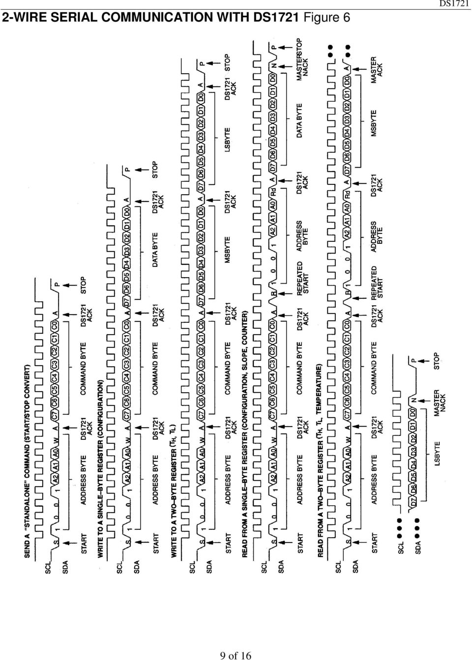
9 2-WIRE SERIAL COMMUNICATION WITH Figure 6 9 of 16
10 SLAVE ADDRESS A control byte is the 1 st byte received following the START condition from the master device. The control byte consists of a 4-bit control code; for the, this is set as 1001 binary for read and write operations. The next 3 bits of the control byte are the device select bits (A2, A1, A0). They are used by the master device to select which of eight devices are to be accessed. The set bits are in effect the 3 least significant bits of the slave address. The last bit of the control byte (R/ W ) defines the operation to be performed. When set to a 1 a read operation is selected, and when set to a 0 a write operation is selected. Following the START condition, the monitors the SDA bus checking the device type identifier being transmitted. Upon receiving the 1001 code and appropriate device select bits, the slave device outputs an acknowledge signal on the SDA line. COMMAND SET Data and control information is read from and written to the in the format shown in Figure 6. To write to the, the master will issue the slave address of the and the R/ W bit will be set to "0". After receiving an acknowledge, the bus master provides a command protocol. After receiving this protocol, the will issue an acknowledge and the master may send data to the. If the is to be read, the master must send the command protocol as before then issue a repeated START condition and the control byte again, this time with the R/ W bit set to "1" to allow reading of the data from the. The command set for the as shown in Table 4 is as follows: Read Temperature [AAh] This command reads the last temperature conversion result from the Thermometer Register in the format described in the OPERATION-Measuring Temperature section. If one s application can accept thermometer resolution of only 1.0 C, the master only must read the first data byte and follow with a NACK and STOP. For higher resolution, both bytes must be read. Access TH [A1h] If R/ W is "0", this command writes to the TH register. After issuing this command, the next 2 bytes written to the, in the format described for thermostat set-points, will set the high temperature threshold for operation of the TOUT output. If R/ W is "1", the value stored in this register is read back. Access TL [A2h] If R/ W is "0", this command writes to the TL register. After issuing this command, the next 2 bytes written to the, in the format described for thermostat set-points, will set the high temperature threshold for operation of the TOUT output. If R/ W is "1", the value stored in this register is read back. Access Config [ACh] If R/ W is "0", this command writes to the configuration register. After issuing this command, the next data byte value is to be written into the configuration register. If R/ W is "1", the next data byte read is the value stored in the configuration register. Start Convert T [51h] This command begins a temperature conversion. No further data is required. In one-shot mode, the temperature conversion will be performed and stored and then the will remain idle. In continuous mode, this command will initiate continuous conversions. 10 of 16
 defines the operation to be performed. When set to a 1 a read operation is selected, and when set to a 0 a write operation is selected.")
11 Stop Convert T [22h] This command stops temperature conversion. No further data is required. This command may be used to halt a in continuous conversion mode. After issuing this command, the current temperature measurement will be completed, stored and the will remain idle until a Start Convert T is issued to resume conversions. COMMAND SET Table 4 INSTRUCTION DESCRIPTION PROTOCOL 2-WIRE BUS DATA AFTER ISSUING NOTES PROTOCOL REGISTER COMMANDS Access Writes to/reads from 8-bit Configuration configuration/status register ACh 1 data byte 1 Access TH Writes to/reads from 12-bit TH register A1h 1 or 2 data bytes 1, 3 Access TL Writes to/reads from 12-bit TL register A2h 1 or 2 data bytes 1, 3 CONVERSION COMMANDS Start Convert T Initiates temperature conversion 51h idle 2 Stop Convert T Terminates continuous conversions 22h idle 2 Read Reads 12-bit Temperature Temperature register AAh Read 1 or 2 data bytes 3 NOTES: 1. Data direction depends upon R/ W bit in the 2-wire control byte. 2. In continuous conversion mode, a Stop Convert T command will halt continuous conversion. To restart, the Start Convert T command must be issued. In one-shot mode, a Start Convert T command must be issued for every temperature reading desired. 3. If the user only desires 8-bit thermometer readings, the master need only read 1 data byte and follow with a NACK and STOP. If higher resolution is required, 2 bytes must be read. 11 of 16

12 SAMPLE COMMAND SEQUENCE Table 5 Example: After power-up, initiates a temperature conversion, bus master reads temperature BUS MASTER DATA (MSB COMMENTS MODE MODE FIRST) TX RX START Bus Master initiates a START condition TX RX <address, 0> Bus Master sends address; R/ W = 0 TX RX 51h Bus Master sends start convert T protocol TX RX START Bus Master initiates a repeated START condition TX RX <address, 0> Bus Master sends address; R/ W = 0 TX RX AAh Bus Master sends read temperature protocol TX RX START Bus Master initiates a repeated START condition TX RX <address, 1> Bus Master sends address; R/ W =1 RX TX <1 data byte> transmits MSB of temperature TX RX ACK Bus Master generates acknowledge bit RX TX <1 data byte> transmits LSB of temperature 12 of 16

13 SAMPLE COMMAND SEQUENCE Table 6 Example: Bus master programs the for 11-bit conversions in the continuous mode with an active low state for the thermostat output. It then programs TH=50 C and TL=45 C and starts temperature conversions. BUS MASTER MODE DATA (MSB COMMENTS MODE FIRST) TX RX START Bus Master initiates a START condition TX RX <address, 0> Bus Master sends address; R/ W = 0 TX RX ACh Bus Master sends access configuration protocol TX RX 08h Bus Master programs configuration register as described above. This will also clear thermostat flags TX RX START Bus Master Initiates a REPEATED START condition TX RX <address, 0> Bus Master sends address; R/ W = 0 TX RX A1h Bus Master sends access TH protocol TX RX 32h Bus Master writes MSB of TH (50 C) TX RX 00h Bus Master writes LSB of TH (50 C) TX RX START Bus Master initiates a REPEATED START condition TX RX <address, 0> Bus Master sends address; R/ W = 0 TX RX A2h Bus Master sends access TL protocol TX RX 2Dh Bus Master writes MSB of TL (45 C) TX RX 00h Bus Master writes LSB of TL (45 C) TX RX START Bus Master initiates a REPEATED START condition TX RX <address, 0> Bus Master sends address; R/ W = 0 TX RX 51h Bus Master sends start convert protocol TX RX STOP Bus Master initiates STOP condition 13 of 16

14 ABSOLUTE MAXIMUM RATINGS* Voltage on VDD, Relative to Ground Voltage on any other pin, Related to Ground Operating Temperature Storage Temperature Soldering Temperature -0.3V to +7.0V -0.3V to +7.0V -55 C to +125 C -55 C to +125 C 260 C for 10 seconds * This is a stress rating only and functional operation of the device at these or any other conditions above those indicated in the operation sections of this specification is not implied. Exposure to absolute maximum rating conditions for extended periods of time may affect reliability. RECOMMENDED DC OPERATING CONDITIONS (-55 C to +125 C; 2.7V V DD 5.5V) PARAMETER SYMBOL CONDITION MIN TYP MAX UNITS NOTES Supply Voltage V DD V 1 DC ELECTRICAL CHARACTERISTICS (-55 C to +125 C; 2.7V V DD 5.5V) PARAMETER SYMBOL CONDITION MIN TYP MAX UNITS NOTES 0.7 V Input Logic High V DD IH V 1 V DD Input Logic Low V IL -0.5 V 1 V DD SDA Output Logic Low Voltage T OUT Output Logic Voltage V OL1 V OL2 V OH V OL 3 ma sink current V 1 6 ma sink current V 1 1 ma source current 2.4 V 1 4 ma sink current 0.4 V 1 0.4V V I/O 0.9 V DD µa 2 Input Current Each I/O Pin I/O Capacitance C I/O 10 pf Standby Current I DD1 1 µa 3, 4 Active Temp. Active Current I DD Conversions Communication only 1000 µa 3, µa 3, 4 14 of 16

15 DC ELECTRICAL CHARACTERISTICS: DIGITAL THERMOMETER (-55 C to +125 C; 2.7V V DD 5.5V) PARAMETER SYMBOL CONDITION MIN TYP MAX UNITS NOTES Thermometer Error T ERR -10 C to +85 C ±1.0 C 5 Resolution 9 12 bits 9-bit Conversions Conversion Time t CONVT 10-bit Conversions bit Conversions ms 12-bit Conversions AC ELECTRICAL CHARACTERISTICS: 2-WIRE INTERFACE (-55 C to +125 C; V DD =2.7V to 5.5V) PARAMETER SYMBOL CONDITION MIN TYP MAX UNITS NOTES SCL Clock Fast Mode f Frequency SCL KHz Standard Mode Bus Free Time Between a STOP Fast Mode 1.3 t and START BUF µs Standard Mode 4.7 Condition Hold Time (Repeated) START Condition Low Period of SCL Clock High Period of SCL Clock Setup Time for a Repeated START Condition t HD:STA t LOW t HIGH t SU:STA Fast Mode Standard Mode Fast Mode Standard Mode Fast Mode Standard Mode Fast Mode Standard Mode Fast Mode Data Hold Time t HD:DAT Standard Mode Fast Mode Data Set-up Time t SU:DAT Rise Time of both SDA and SCL Signals t R Standard Mode Fast Mode Standard Mode C B µs 6 µs µs µs 0.9 µs 7 ns 8 ns 8 Fall Time of both Fast Mode SDA and SCL t F Standard Mode C Signals B 1000 ns 9 Set-up time for Fast Mode 0.6 t STOP Condition SU:STO Standard Mode 4.0 µs Capacitive Load for each Bus Line C b 400 pf 9 Input Capacitance C I 5 pf 15 of 16
 PARAMETER SYMBOL CONDITION MIN TYP MAX UNITS NOTES SCL Clock Fast Mode 0 400 f Frequency SCL KHz Standard Mode 0 100 Bus Free Time Between a STOP Fast Mode 1.3 t and START BUF µs Standard Mode 4.")
16 NOTES: 1. All voltages are referenced to ground. 2. I/O pins of fast mode devices must not obstruct the SDA and SCL lines if V DD is switched off. 3. I DD specified with T OUT pin open. 4. I DD specified with V DD at 5.0V and SDA,SCL = 5.0V, 0 C to 70 C. 5. See typical accuracy curves for specification limits outside the temperature range indicated. 6. After this period, the first clock pulse is generated. 7. The maximum t HD:DAT has only to be met if the device does not stretch the LOW period (t LOW ) of the SCL signal. 8. A fast mode device can be used in a standard mode system, but the requirement t SU:DAT >250 ns must then be met. This will automatically be the case if the device does not stretch the LOW period of the SCL signal. If such a device does stretch the LOW period of the SCL signal, it must output the next data bit to the SDA line t R MAX+t SU:DAT = 1250 ns before the SCL line is released. 9. C b - total capacitance of one bus line in pf. TIMING DIAGRAMS Figure 7 TYPICAL THERMOMETER PERFORMANCE CURVE Figure 8 TBD 16 of 16

DS1621 Digital Thermometer and Thermostat
 www.maxim-ic.com FEATURES Temperature measurements require no external components Measures temperatures from -55 C to +125 C in 0.5 C increments. Fahrenheit equivalent is -67 F to 257 F in 0.9 F increments
DS1621 Digital Thermometer and Thermostat
 Digital Thermometer and Thermostat www.dalsemi.com FEATURES Temperature measurements require no external components Measures temperatures from 55 C to +125 C in 0.5 C increments. Fahrenheit equivalent
DS1821 Programmable Digital Thermostat and Thermometer
 ma www.maxim-ic.com FEATURES Requires no external components Unique 1-Wire interface requires only one port pin for communication Operates over a -55 C to +125 C (67 F to +257 F) temperature range Functions
DS18B20 Programmable Resolution 1-Wire Digital Thermometer
 www.dalsemi.com FEATURES Unique 1-Wire interface requires only one port pin for communication Multidrop capability simplifies distributed temperature sensing applications Requires no external components
DS1307ZN. 64 x 8 Serial Real-Time Clock
 DS137 64 x 8 Serial Real-Time Clock www.maxim-ic.com FEATURES Real-time clock (RTC) counts seconds, minutes, hours, date of the month, month, day of the week, and year with leap-year compensation valid
FM75 Low-Voltage Two-Wire Digital Temperature Sensor with Thermal Alarm
 Low-Voltage Two-Wire Digital Temperature Sensor with Thermal Alarm Features User Configurable to 9, 10, 11 or 12-bit Resolution Precision Calibrated to ±1 C, 0 C to 100 C Typical Temperature Range: -40
PACKAGE OUTLINE DALLAS DS2434 DS2434 GND. PR 35 PACKAGE See Mech. Drawings Section
 PRELIMINARY DS2434 Battery Identification Chip FEATURES Provides unique ID number to battery packs PACKAGE OUTLINE Eliminates thermistors by sensing battery temperature on chip DALLAS DS2434 1 2 3 256
LM75 Digital Temperature Sensor and Thermal Watchdog with Two-Wire Interface
 Digital Temperature Sensor and Thermal Watchdog with Two-Wire Interface General Description The LM75 is a temperature sensor, Delta-Sigma analog-todigital converter, and digital over-temperature detector
64 x 8, Serial, I 2 C Real-Time Clock
 DS1307 64 x 8, Serial, I 2 C Real-Time Clock GENERAL DESCRIPTION The DS1307 serial real-time clock (RTC) is a lowpower, full binary-coded decimal (BCD) clock/calendar plus 56 bytes of NV SRAM. Address
NTE2053 Integrated Circuit 8 Bit MPU Compatible A/D Converter
 NTE2053 Integrated Circuit 8 Bit MPU Compatible A/D Converter Description: The NTE2053 is a CMOS 8 bit successive approximation Analog to Digital converter in a 20 Lead DIP type package which uses a differential
HDMM01 V1.0. Dual-axis Magnetic Sensor Module With I 2 C Interface FEATURES. Signal Path X
 Dual-axis Magnetic Sensor Module With I 2 C Interface FEATURES Low power consumption: typically 0.4mA@3V with 50 measurements per second Power up/down function available through I 2 C interface SET/RESET
DS1232LP/LPS Low Power MicroMonitor Chip
 DSLP/LPS Low Power MicroMonitor Chip www.dalsemi.com FEATURES Super-low power version of DS 50 µa quiescent current Halts and restarts an out-of-control microprocessor Automatically restarts microprocessor
PCT2075. 1. General description. I 2 C-bus Fm+, 1 degree C accuracy, digital temperature sensor and thermal watchdog
 I 2 C-bus Fm+, 1 degree C accuracy, digital temperature sensor and thermal watchdog Rev. 9 24 October 2014 Product data sheet 1. General description The is a temperature-to-digital converter featuring
DS2401 Silicon Serial Number
 19-5860; Rev 3/15 Silicon Serial Number BENEFITS AND FEATURES Guaranteed Unique 64-Bit ROM ID Chip for Absolute Traceability o Unique, Factory-Lasered and Tested 64-Bit Registration Number (8-Bit Family
LM75A. 1. General description. 2. Features. Digital temperature sensor and thermal watchdog
 Rev. 04 10 July 2007 Product data sheet 1. General description 2. Features The is a temperature-to-digital converter using an on-chip band gap temperature sensor and Sigma-delta A-to-D conversion technique.
7 OUT1 8 OUT2 9 OUT3 10 OUT4 11 OUT5 12 OUT6 13 OUT7 14 OUT8 15 OUT9 16 OUT10 17 OUT11 18 OUT12 19 OUT13 20 OUT14 21 OUT15 22 OUT16 OUT17 23 OUT18
 18 CHANNELS LED DRIVER GENERAL DESCRIPTION IS31FL3218 is comprised of 18 constant current channels each with independent PWM control, designed for driving LEDs. The output current of each channel can be
Cold-Junction-Compensated K-Thermocoupleto-Digital Converter (0 C to +1024 C)
") 19-2235; Rev 1; 3/02 Cold-Junction-Compensated K-Thermocoupleto-Digital General Description The performs cold-junction compensation and digitizes the signal from a type-k thermocouple. The data is output
19-2235; Rev 1; 3/02 Cold-Junction-Compensated K-Thermocoupleto-Digital General Description The performs cold-junction compensation and digitizes the signal from a type-k thermocouple. The data is output
MMC314xMR. Ultra Small 3-axis Magnetic Sensor, With I 2 C Interface. Signal Path X. Signal Path Y. Signal Path Z FEATURES
 Ultra Small 3-axis Magnetic Sensor, With I 2 C Interface MMC314xMR FEATURES Full integration of 3-axis magnetic sensors and electronics circuits resulting in less external components needed Small Low profile
PCA9564 Parallel bus to I 2 C-bus controller INTEGRATED CIRCUITS. 2006 Sep 01. Product data sheet Supersedes data of 2004 Jun 25
 INTEGRATED CIRCUITS Supersedes data of 2004 Jun 25 2006 Sep 01 Philips Semiconductors FEATURES Parallel-bus to I 2 C-bus protocol converter and interface Both master and slave functions Multi-master capability
2-wire Serial EEPROM AT24C512
 Features Low-voltage and Standard-voltage Operation 5.0 (V CC = 4.5V to 5.5V). (V CC =.V to 5.5V). (V CC =.V to.v) Internally Organized 5,5 x -wire Serial Interface Schmitt Triggers, Filtered Inputs for
DS1220Y 16k Nonvolatile SRAM
 Not Recommended for New Design DS122Y 16k Nonvolatile SRAM www.maxim-ic.com FEATURES years minimum data retention in the absence of external power Data is automatically protected during power loss Directly
HT1632C 32 8 &24 16 LED Driver
 328 &216 LED Driver Features Operating voltage: 2.V~5.5V Multiple LED display 32 ROW /8 COM and 2 ROW & 16 COM Integrated display RAM select 32 ROW & 8 COM for 6 display RAM, or select 2 ROW & 16 COM for
LM75 Digital Temperature Sensor and Thermal Watchdog with Two-Wire Interface
 LM75 Digital Temperature Sensor and Thermal Watchdog with Two-Wire Interface General Description The LM75 is a temperature sensor, Delta-Sigma analog-to-digital converter, and digital over-temperature
LC898300XA. Functions Automatic adjustment to the individual resonance frequency Automatic brake function Initial drive frequency adjustment function
 Ordering number : A2053 CMOS LSI Linear Vibrator Driver IC http://onsemi.com Overview is a Linear Vibrator Driver IC for a haptics and a vibrator installed in mobile equipments. The best feature is it
MicroMag3 3-Axis Magnetic Sensor Module
 1008121 R01 April 2005 MicroMag3 3-Axis Magnetic Sensor Module General Description The MicroMag3 is an integrated 3-axis magnetic field sensing module designed to aid in evaluation and prototyping of PNI
ABRIDGED DATA SHEET EVALUATION KIT AVAILABLE
 EVALUATION KIT AVAILABLE General Description DeepCoverM embedded security solutions cloak sensitive data under multiple layers of advanced physical security to provide the most secure key storage possible.
DS1225Y 64k Nonvolatile SRAM
 DS1225Y 64k Nonvolatile SRAM www.maxim-ic.com FEATURES years minimum data retention in the absence of external power Data is automatically protected during power loss Directly replaces 2k x 8 volatile
Spread-Spectrum Crystal Multiplier DS1080L. Features
 Rev 1; 3/0 Spread-Spectrum Crystal Multiplier General Description The is a low-jitter, crystal-based clock generator with an integrated phase-locked loop (PLL) to generate spread-spectrum clock outputs
TRIPLE PLL FIELD PROG. SPREAD SPECTRUM CLOCK SYNTHESIZER. Features
 DATASHEET ICS280 Description The ICS280 field programmable spread spectrum clock synthesizer generates up to four high-quality, high-frequency clock outputs including multiple reference clocks from a low-frequency
DS1220Y 16k Nonvolatile SRAM
 19-5579; Rev 10/10 NOT RECOENDED FOR NEW DESIGNS 16k Nonvolatile SRAM www.maxim-ic.com FEATURES 10 years minimum data retention in the absence of external power Data is automatically protected during power
W25Q80, W25Q16, W25Q32 8M-BIT, 16M-BIT AND 32M-BIT SERIAL FLASH MEMORY WITH DUAL AND QUAD SPI
 8M-BIT, 16M-BIT AND 32M-BIT SERIAL FLASH MEMORY WITH DUAL AND QUAD SPI - 1 - Preliminary - Revision B Table of Contents 1. GENERAL DESCRIPTION... 5 2. FEATURES... 5 3. PIN CONFIGURATION SOIC 208-MIL...
DS1678 Real-Time Event Recorder
 DS1678 Real-Time Event Recorder www.maxim-ic.com GENERAL DESCRIPTION The DS1678 real-time clock (RTC) event recorder records the time and date of a nonperiodic, asynchronous event each time the INT pin
NB3H5150 I2C Programming Guide. I2C/SMBus Custom Configuration Application Note
 NB3H550 I2C Programming Guide I2C/SMBus Custom Configuration Application Note 3/4/206 Table of Contents Introduction... 3 Overview Process of Configuring NB3H550 via I2C/SMBus... 3 Standard I2C Communication
Develop a Dallas 1-Wire Master Using the Z8F1680 Series of MCUs
 Develop a Dallas 1-Wire Master Using the Z8F1680 Series of MCUs AN033101-0412 Abstract This describes how to interface the Dallas 1-Wire bus with Zilog s Z8F1680 Series of MCUs as master devices. The Z8F0880,
DS18B20-PAR 1-Wire Parasite-Power Digital Thermometer
 www.maxim-ic.com FEATURES Unique 1-Wire interface requires only one port pin for communication Derives power from data line ( parasite power ) does not need a local power supply Multi-drop capability simplifies
10-Bit Digital Temperature Sensor (AD7416) and Four/Single-Channel ADC (AD7417/AD7418) AD7416/AD7417/AD7418
 and Four/Single-Channel ADC (AD7417/AD7418) AD7416/AD7417/AD7418") a FEATURES 10-Bit ADC with 15 s and 30 s Conversion Times Single and Four Single-Ended Analog Input Channels On-Chip Temperature Sensor: 55 C to +125 C On-Chip Track/Hold Over-Temperature Indicator Automatic
a FEATURES 10-Bit ADC with 15 s and 30 s Conversion Times Single and Four Single-Ended Analog Input Channels On-Chip Temperature Sensor: 55 C to +125 C On-Chip Track/Hold Over-Temperature Indicator Automatic
INTEGRATED CIRCUITS DATA SHEET. PCF8591 8-bit A/D and D/A converter. Product specification Supersedes data of 2001 Dec 13.
 INTEGRATED CIRCUITS DATA SHEET Supersedes data of 2001 Dec 13 2003 Jan 27 CONTENTS 1 FEATURES 2 APPLICATIONS 3 GENERAL DESCRIPTION 4 ORDERING INFORMATION 5 BLOCK DIAGRAM 6 PINNING 7 FUNCTIONAL DESCRIPTION
NCP1840. 8-Channel Programmable LED Driver
 8-Channel Programmable LED Driver The NCP1840 is a general purpose LED driver that allows for full programmability of eight separate LED channels through a simple I 2 C serial communication interface.
Part Number Description Packages available
 Features 3 digital I/O Serial Data output Connects directly to RF Modules Easy Enc / Dec Pairing Function Minimal External Components Required Performs all encoding/decoding of data for Reliable Operation.
Allows the user to protect against inadvertent write operations. Device select and address bytes are Acknowledged Data Bytes are not Acknowledged
 Write Protect CAT24WCxxx I 2 C Serial EEPROMs. Allows the user to protect against inadvertent write operations. WP = V CC : Write Protected Device select and address bytes are Acknowledged Data Bytes are
LM95231 Precision Dual Remote Diode Temperature Sensor with SMBus Interface and TruTherm Technology
 Precision Dual Remote Diode Temperature Sensor with SMBus Interface and TruTherm Technology General Description The is a precision dual remote diode temperature sensor (RDTS) that uses National s TruTherm
The I2C Bus. NXP Semiconductors: UM10204 I2C-bus specification and user manual. 14.10.2010 HAW - Arduino 1
 The I2C Bus Introduction The I2C-bus is a de facto world standard that is now implemented in over 1000 different ICs manufactured by more than 50 companies. Additionally, the versatile I2C-bus is used
HP03 BAROMETER MODULE 2007-1-17 Version: 1.1
 . Integrated pressure sensor. Pressure Range 300-1100hpa. 16 Bit Σ Δ ADC. 11 coefficients for software compensation stored on chip. I 2 C Serial Interface. One system clock line (32768Hz). One hardware
8-Bit Flash Microcontroller for Smart Cards. AT89SCXXXXA Summary. Features. Description. Complete datasheet available under NDA
 Features Compatible with MCS-51 products On-chip Flash Program Memory Endurance: 1,000 Write/Erase Cycles On-chip EEPROM Data Memory Endurance: 100,000 Write/Erase Cycles 512 x 8-bit RAM ISO 7816 I/O Port
SE95. 1. General description. Ultra high accuracy digital temperature sensor and thermal watchdog
 Ultra high accuracy digital temperature sensor and thermal watchdog Rev. 07 2 September 2009 Product data sheet 1. General description The is a temperature-to-digital converter using an on-chip band gap
ICS514 LOCO PLL CLOCK GENERATOR. Description. Features. Block Diagram DATASHEET
 DATASHEET ICS514 Description The ICS514 LOCO TM is the most cost effective way to generate a high-quality, high-frequency clock output from a 14.31818 MHz crystal or clock input. The name LOCO stands for
M25P40 3V 4Mb Serial Flash Embedded Memory
 Features M25P40 3V 4Mb Serial Flash Embedded Memory Features SPI bus-compatible serial interface 4Mb Flash memory 75 MHz clock frequency (maximum) 2.3V to 3.6V single supply voltage Page program (up to
DM74LS191 Synchronous 4-Bit Up/Down Counter with Mode Control
 August 1986 Revised February 1999 DM74LS191 Synchronous 4-Bit Up/Down Counter with Mode Control General Description The DM74LS191 circuit is a synchronous, reversible, up/ down counter. Synchronous operation
DS1990A-F5. Serial Number ibutton TM
 www.dalsemi.com SPECIAL FEATURES Upgrade of DS1990 allows multiple Serial Number ibuttons to reside on a common bus Unique 48 bit serial number Low-cost electronic key for access control 8-bit CRC for
DS2786 Stand-Alone OCV-Based Fuel Gauge
 19-4637; 5/09 www.maxim-ic.com GENERAL DESCRIPTION The DS2786 estimates available capacity for rechargeable Li-Ion and Li-Ion Polymer batteries based on the cell voltage in the open-circuit state following
256K (32K x 8) Static RAM
 Static RAM") 256K (32K x 8) Static RAM Features High speed: 55 ns and 70 ns Voltage range: 4.5V 5.5V operation Low active power (70 ns, LL version) 275 mw (max.) Low standby power (70 ns, LL version) 28 µw (max.) Easy
256K (32K x 8) Static RAM Features High speed: 55 ns and 70 ns Voltage range: 4.5V 5.5V operation Low active power (70 ns, LL version) 275 mw (max.) Low standby power (70 ns, LL version) 28 µw (max.) Easy
Serial Communications
 Serial Communications 1 Serial Communication Introduction Serial communication buses Asynchronous and synchronous communication UART block diagram UART clock requirements Programming the UARTs Operation
M24512-W M24512-R M24512-HR M24256-BW M24256-BR M24256-BHR
 M24512-W M24512-R M24512-HR M24256-BW M24256-BR M24256-BHR 512 Kbit and 256 Kbit serial I²C bus EEPROM with three Chip Enable lines Features Two-wire I 2 C serial interface supports the 1 MHz protocol
High-Speed, Low r ON, SPST Analog Switch (1-Bit Bus Switch)
") High-Speed, Low r ON, SPST Analog Switch (1-Bit Bus Switch) DG2301 ishay Siliconix DESCRIPTION The DG2301 is a high-speed, 1-bit, low power, TTLcompatible bus switch. Using sub-micron CMOS technology,
High-Speed, Low r ON, SPST Analog Switch (1-Bit Bus Switch) DG2301 ishay Siliconix DESCRIPTION The DG2301 is a high-speed, 1-bit, low power, TTLcompatible bus switch. Using sub-micron CMOS technology,
MCP4017/18/19. 7-Bit Single I 2 C Digital POT with Volatile Memory in SC70. Package Types. Features. Device Features. Rheostat
 7-Bit Single I 2 C Digital POT with Volatile Memory in SC7 Features Potentiometer or Rheostat configuration options 7-bit: Resistor Network Resolution - 127 Resistors (128 Steps) Zero Scale to Full Scale
DG2302. High-Speed, Low r ON, SPST Analog Switch. Vishay Siliconix. (1-Bit Bus Switch with Level-Shifter) RoHS* COMPLIANT DESCRIPTION FEATURES
 RoHS* COMPLIANT DESCRIPTION FEATURES") High-Speed, Low r ON, SPST Analog Switch (1-Bit Bus Switch with Level-Shifter) DG2302 DESCRIPTION The DG2302 is a high-speed, 1-bit, low power, TTLcompatible bus switch. Using sub-micron CMOS technology,
High-Speed, Low r ON, SPST Analog Switch (1-Bit Bus Switch with Level-Shifter) DG2302 DESCRIPTION The DG2302 is a high-speed, 1-bit, low power, TTLcompatible bus switch. Using sub-micron CMOS technology,
1-to-8 I 2 C Bus Switches/Multiplexers with Bus Lock-Up Detection, Isolation, and Notification
 19-4207; Rev 0; 9/08 EVALUATION KIT AVAILABLE 1-to-8 I 2 C Bus Switches/Multiplexers with Bus General Description The 8-channel I 2 C switches/multiplexers expand the main I 2 C bus to any combination
8254 PROGRAMMABLE INTERVAL TIMER
 PROGRAMMABLE INTERVAL TIMER Y Y Y Compatible with All Intel and Most Other Microprocessors Handles Inputs from DC to 10 MHz 8 MHz 8254 10 MHz 8254-2 Status Read-Back Command Y Y Y Y Y Six Programmable
BATRON. Specification for BTHQ 21605V-FSTF-I2C-COG
 BATRON Specification for BTHQ 21605V-FSTF-I2C-COG Version October 2003 PAGE 2 OF 12 DOCUMENT REVISION HISTORY 1: DOCUMENT REVISION FROM TO DATE DESCRIPTION CHANGED BY CHECKED BY A 2003.10.16 First release.
AN141 SMBUS COMMUNICATION FOR SMALL FORM FACTOR DEVICE FAMILIES. 1. Introduction. 2. Overview of the SMBus Specification. 2.1.
 SMBUS COMMUNICATION FOR SMALL FORM FACTOR DEVICE FAMILIES 1. Introduction C8051F3xx and C8051F41x devices are equipped with an SMBus serial I/O peripheral that is compliant with both the System Management
DALLAS DS1233 Econo Reset. BOTTOM VIEW TO-92 PACKAGE See Mech. Drawings Section on Website
 5V EconoReset www.maxim-ic.com FEATURES Automatically restarts microprocessor after power failure Monitors pushbutton for external override Internal circuitry debounces pushbutton switch Maintains reset
CD4013BC Dual D-Type Flip-Flop
 CD4013BC Dual D-Type Flip-Flop General Description The CD4013B dual D-type flip-flop is a monolithic complementary MOS (CMOS) integrated circuit constructed with N- and P-channel enhancement mode transistors.
CAT28C64B F R E E. 64K-Bit CMOS PARALLEL EEPROM L E A D FEATURES DESCRIPTION BLOCK DIAGRAM
 64K-Bit CMOS PARALLEL EEPROM FEATURES Fast read access times: 90/120/150ns Low power CMOS dissipation: Active: 25 ma max. Standby: 100 µa max. Simple write operation: On-chip address and data latches Self-timed
Serial Communications / Protocol in AirTest Products
 Serial Communications / Protocol in AirTest Products General The standard sensor has two different ways of serial communication with sensor s peripherals and the outside world. One is through the UART
DATA SHEET. TDA1543 Dual 16-bit DAC (economy version) (I 2 S input format) INTEGRATED CIRCUITS
 (I 2 S input format) INTEGRATED CIRCUITS") INTEGRATED CIRCUITS DATA SHEET File under Integrated Circuits, IC01 February 1991 FEATURES Low distortion 16-bit dynamic range 4 oversampling possible Single 5 V power supply No external components required
INTEGRATED CIRCUITS DATA SHEET File under Integrated Circuits, IC01 February 1991 FEATURES Low distortion 16-bit dynamic range 4 oversampling possible Single 5 V power supply No external components required
Two-wire Automotive Serial EEPROM AT24C01A AT24C02 AT24C04 AT24C08 (1) AT24C16 (2)
 AT24C16 (2)") Features Medium-voltage and Standard-voltage Operation 5.0 (V CC = 4.5V to 5.5V) 2.7 (V CC = 2.7V to 5.5V) Internally Organized 128 x 8 (1K), 256 x 8 (2K), 512 x 8 (4K), 1024 x 8 (8K) or 2048 x 8 (16K)
Features Medium-voltage and Standard-voltage Operation 5.0 (V CC = 4.5V to 5.5V) 2.7 (V CC = 2.7V to 5.5V) Internally Organized 128 x 8 (1K), 256 x 8 (2K), 512 x 8 (4K), 1024 x 8 (8K) or 2048 x 8 (16K)
YAS532B MS-3R Magnetic Field Sensor Type 3R
 MS-3R Magnetic Field Sensor Type 3R Overview The is a 3-axis geomagnetic sensor device with the following circuits integrated on one chip: a buffer amplifier, an AD converter, a clock generator circuit,
High-Speed, 5 V, 0.1 F CMOS RS-232 Driver/Receivers ADM202/ADM203
 a FEATURES kb Transmission Rate ADM: Small (. F) Charge Pump Capacitors ADM3: No External Capacitors Required Single V Power Supply Meets EIA-3-E and V. Specifications Two Drivers and Two Receivers On-Board
LC7218, 7218M, 7218JM
 Ordering number : EN4758B CMOS LSI LC7218, 7218M, 7218JM PLL Frequency Synthesizer for Electronic Tuning in AV Systems Overview The LC7218, LC7218M and LC7218JM are PLL frequency synthesizers for electronic
PCAN-MicroMod Universal I/O Module with CAN Interface. User Manual. Document version 2.1.0 (2014-01-16)
") PCAN-MicroMod Universal I/O Module with CAN Interface User Manual Document version 2.1.0 (2014-01-16) Products taken into account Product Name Part number Model PCAN-MicroMod IPEH-002080 with firmware
PCAN-MicroMod Universal I/O Module with CAN Interface User Manual Document version 2.1.0 (2014-01-16) Products taken into account Product Name Part number Model PCAN-MicroMod IPEH-002080 with firmware
SPREAD SPECTRUM CLOCK GENERATOR. Features
 DATASHEET ICS7152 Description The ICS7152-01, -02, -11, and -12 are clock generators for EMI (Electro Magnetic Interference) reduction (see below for frequency ranges and multiplier ratios). Spectral peaks
Bi-directional level shifter for I²C-bus and other systems.
 APPLICATION NOTE Bi-directional level shifter for I²C-bus and other Abstract With a single MOS-FET a bi-directional level shifter circuit can be realised to connect devices with different supply voltages
NJU6061. Full Color LED Controller Driver with PWM Control GENERAL DESCRIPTION PACKAGE OUTLINE FEATURES
 Full Color LED Controller Driver with PWM Control GENERAL DESCRIPTION The NJU6061 is a full color LED controller driver. It can control and drive a 3 in 1 packaged (Red, Green and Blue) LED. The NJU6061
HD61202U. (Dot Matrix Liquid Crystal GraphicDisplay Column Driver)
") HD622U (Dot Matrix Liquid Crystal GraphicDisplay Column Driver) Description HD622U is a column (segment) driver for dot matrix liquid crystal graphic display systems. It stores the display data transferred
HD622U (Dot Matrix Liquid Crystal GraphicDisplay Column Driver) Description HD622U is a column (segment) driver for dot matrix liquid crystal graphic display systems. It stores the display data transferred
ADT7467. dbcool Remote Thermal Monitor and Fan Controller
 dbcool Remote Thermal Monitor and Fan Controller The ADT7467 dbcool controller is a thermal monitor and multiple fan controller for noise-sensitive or power-sensitive applications requiring active system
TDA7448 6 CHANNEL VOLUME CONTROLLER 1 FEATURES 2 DESCRIPTION. Figure 1. Package
 6 CHANNEL CONTROLLER FEATURES 6 CHANNEL INPUTS 6 CHANNEL OUTPUTS ATTENUATION RANGE OF 0 TO -79dB CONTROL IN.0dB STEPS 6 CHANNEL INDEPENDENT CONTROL ALL FUNCTION ARE PROGRAMMABLE VIA SERIAL BUS DESCRIPTION
1 TO 4 CLOCK BUFFER ICS551. Description. Features. Block Diagram DATASHEET
 DATASHEET 1 TO 4 CLOCK BUFFER ICS551 Description The ICS551 is a low cost, high-speed single input to four output clock buffer. Part of IDT s ClockBlocks TM family, this is our lowest cost, small clock
LM75B. 1. General description. 2. Features and benefits. Digital temperature sensor and thermal watchdog
 Rev. 6.1 6 February 2015 Product data sheet 1. General description The is a temperature-to-digital converter using an on-chip band gap temperature sensor and Sigma-Delta A-to-D conversion technique with
1-Mbit (128K x 8) Static RAM
 Static RAM") 1-Mbit (128K x 8) Static RAM Features Pin- and function-compatible with CY7C109B/CY7C1009B High speed t AA = 10 ns Low active power I CC = 80 ma @ 10 ns Low CMOS standby power I SB2 = 3 ma 2.0V Data Retention
1-Mbit (128K x 8) Static RAM Features Pin- and function-compatible with CY7C109B/CY7C1009B High speed t AA = 10 ns Low active power I CC = 80 ma @ 10 ns Low CMOS standby power I SB2 = 3 ma 2.0V Data Retention
DS2187 Receive Line Interface
 Receive Line Interface www.dalsemi.com FEATURES Line interface for T1 (1.544 MHz) and CEPT (2.048 MHz) primary rate networks Extracts clock and data from twisted pair or coax Meets requirements of PUB
Real Time Clock Module with I2C Bus
 Moisture Seitivity Level: MSL=1 FEATURES: With state-of-the-art RTC Technology by Micro Crystal AG RTC module with built-in crystal oscillating at 32.768 khz 3 timekeeping current at 3 Timekeeping down
MCP3426/7/8. 16-Bit, Multi-Channel ΔΣ Analog-to-Digital Converter with I 2 C Interface and On-Board Reference. Features.
 16-Bit, Multi-Channel ΔΣ Analog-to-Digital Converter with I 2 C Interface and On-Board Reference Features 16-bit ΔΣ ADC with Differential Inputs: - 2 channels: MCP3426 and MCP3427-4 channels: MCP3428 Differential
UV A Light Sensor with I 2 C Interface
 UV A Light Sensor with I 2 C Interface DESCRIPTION is an advanced ultraviolet (UV) light sensor with I 2 C protocol interface and designed by the CMOS process. It is easily operated via a simple I 2 C
USB2.0 <=> I2C V4.4. Konverter Kabel und Box mit Galvanischetrennung
 USB2.0 I2C V4.4 Konverter Kabel und Box mit Galvanischetrennung USB 2.0 I2C Konverter Kabel V4.4 (Prod. Nr. #210) USB Modul: Nach USB Spezifikation 2.0 & 1.1 Unterstützt automatisch "handshake
UM10204. I 2 C-bus specification and user manual. Document information
 Rev. 6 4 April 2014 User manual Document information Info Keywords Abstract Content I2C, I2C-bus, Standard-mode, Fast-mode, Fast-mode Plus, Fm+, Ultra Fast-mode, UFm, High Speed, Hs, inter-ic, SDA, SCL,
Sierra Dual 24 Volt Brushless DC Motor Controller Product Specification
 Sierra Dual 24 Volt Brushless DC Motor Controller Product Specification Assembly 025A0215 600A0942 Rev. A May 14, 2012 025A0215 Brushless DC Motor Controller Page 1 Revision History ECN # Date Rev Description
-80E PC2-6400 800 800 533 400 12.5 12.5 55-667 PC2-5300 667 533 400 15 15 55-53E PC2-4200 533 400 15 15 55
 SDRAM FBDIMM MT18HTF12872FDZ 1GB MT18HTF25672FDZ 2GB 1GB, 2GB (x72, DR) 240-Pin SDRAM FBDIMM Features Features 240-pin, fully buffered dual in-line memory module (FBDIMM) Fast data transfer rates: PC2-4200,
ICS379. Quad PLL with VCXO Quick Turn Clock. Description. Features. Block Diagram
 Quad PLL with VCXO Quick Turn Clock Description The ICS379 QTClock TM generates up to 9 high quality, high frequency clock outputs including a reference from a low frequency pullable crystal. It is designed
AND8336. Design Examples of On Board Dual Supply Voltage Logic Translators. Prepared by: Jim Lepkowski ON Semiconductor. http://onsemi.
 Design Examples of On Board Dual Supply Voltage Logic Translators Prepared by: Jim Lepkowski ON Semiconductor Introduction Logic translators can be used to connect ICs together that are located on the
css Custom Silicon Solutions, Inc.
 css Custom Silicon Solutions, Inc. GENERAL PART DESCRIPTION The is a micropower version of the popular timer IC. It features an operating current under µa and a minimum supply voltage of., making it ideal
Elettronica dei Sistemi Digitali Costantino Giaconia SERIAL I/O COMMON PROTOCOLS
 SERIAL I/O COMMON PROTOCOLS RS-232 Fundamentals What is RS-232 RS-232 is a popular communications interface for connecting modems and data acquisition devices (i.e. GPS receivers, electronic balances,
DDR2 SDRAM FBDIMM MT36HTF25672F 2GB MT36HTF51272F 4GB. Features. 2GB, 4GB (x72, DR) 240-Pin DDR2 SDRAM FBDIMM. Features
 240-Pin DDR2 SDRAM FBDIMM. Features") SDRAM FBDIMM MT36HTF25672F 2GB MT36HTF51272F 4GB 2GB, 4GB (x72, DR) 240-Pin SDRAM FBDIMM Features Features 240-pin, fully buffered DIMM (FBDIMM) Fast data transfer rates: PC2-4200, PC2-5300, or PC2-6400
SDRAM FBDIMM MT36HTF25672F 2GB MT36HTF51272F 4GB 2GB, 4GB (x72, DR) 240-Pin SDRAM FBDIMM Features Features 240-pin, fully buffered DIMM (FBDIMM) Fast data transfer rates: PC2-4200, PC2-5300, or PC2-6400
1 Wire TM Digital Thermometer
 DS1820 1 Wire TM Digital Thermometer FEATURES Unique 1 Wire TM interface requires only one port pin for communication Multidrop capability simplifies distributed temperature sensing applications Requires
HCC/HCF4032B HCC/HCF4038B
 HCC/HCF4032B HCC/HCF4038B TRIPLE SERIAL ADDERS INERT INPUTS ON ALL ADDERS FOR SUM COMPLEMENTING APPLICATIONS FULLY STATIC OPERATION...DC TO 10MHz (typ.) @ DD = 10 BUFFERED INPUTS AND OUTPUTS SINGLE-PHASE
DS12887. Real Time Clock FEATURES PIN ASSIGNMENT PIN DESCRIPTION
 DS12887 Real Time Clock FEATURES Drop in replacement for IBM AT computer clock/ calendar Pin compatible with the MC146818B and DS1287 Totally nonvolatile with over 10 years of operation in the absence
udrive-usd-g1 Embedded DOS micro-drive Module Data Sheet
 4D SYSTEMS udrie-usd-g1 Embedded DOS micro-drive Module Document Date: 2nd April 2009 Document Revision: 2.0 Page 1 of 9 udrie-usd-g1 Embedded DOS micro-drive 4D SYSTEMS Description Features The is an
24-Bit Analog-to-Digital Converter (ADC) for Weigh Scales FEATURES S8550 VFB. Analog Supply Regulator. Input MUX. 24-bit Σ ADC. PGA Gain = 32, 64, 128
 for Weigh Scales FEATURES S8550 VFB. Analog Supply Regulator. Input MUX. 24-bit Σ ADC. PGA Gain = 32, 64, 128") 24-Bit Analog-to-Digital Converter (ADC) for Weigh Scales DESCRIPTION Based on Avia Semiconductor s patented technology, HX711 is a precision 24-bit analogto-digital converter (ADC) designed for weigh
24-Bit Analog-to-Digital Converter (ADC) for Weigh Scales DESCRIPTION Based on Avia Semiconductor s patented technology, HX711 is a precision 24-bit analogto-digital converter (ADC) designed for weigh
Internal Oscillator. I 2 C Interface. SPI Interface. Controller. Internal Registers Port Controller. Eight I/O Pins. Figure 1.
 SPI TO I 2 C BRIDGE AND GPIO PORT EXPANDER Single Chip SPI to I 2 C Transfer Integrated clock; no external clock required On-Chip Voltage Monitor Slave Serial Peripheral Interface (SPI) Up to 1.0 Mbit/s
MR25H10. RoHS FEATURES INTRODUCTION
 FEATURES No write delays Unlimited write endurance Data retention greater than 20 years Automatic data protection on power loss Block write protection Fast, simple SPI interface with up to 40 MHz clock
www.jameco.com 1-800-831-4242
 Distributed by: www.jameco.com 1-800-831-4242 The content and copyrights of the attached material are the property of its owner. www.maxim-ic.com FEATURES 10 years minimum data retention in the absence