MPQ4420 High Efficiency 2A, 36V, Synchronous Step-Down Converter AEC-Q100 Qualified
|
|
|
- Rosamund Clarke
- 7 years ago
- Views:
Transcription
1 The Future of Analog IC Technology DESCRIPTION The MPQ4420 is a high-frequency, synchronous, rectified, step-down, switch-mode converter with built-in power MOSFETs. It offers a very compact solution to achieve a 2A continuous output current with excellent load and line regulation over a wide input supply range. The MPQ4420 has synchronous mode operation for higher efficiency over the output current load range. Current-mode operation provides fast transient response and eases loop stabilization. Full protection features include over-current protection and thermal shut down. The MPQ4420 requires a minimal number of readily-available standard external components, and is available in a space-saving 8-pin TSOT23 package. MPQ4420 High Efficiency 2A, 36V, Synchronous Step-Down Converter AEC-Q100 Qualified FEATURES Wide 4V to 30V Continuous Operating Input Range 36V Input Transient Tolerance for Automotive Load Dump 90mΩ/55mΩ Low R DS(ON) Internal Power MOSFETs High-Efficiency Synchronous Mode Operation Default 410kHz Switching Frequency Synchronizes to a 200kHz to 2.2MHz External Clock High Duty Cycle for Automotive Cold-crank Power-Save Mode Internal Soft-Start Power Good OCP Protection and Hiccup Thermal Shutdown Output Adjustable from 0.8V Available in an 8-pin TSOT-23 package Available in AEC-Q100 Grade 1 APPLICATIONS Automotive Industrial Control System Distributed Power Systems All MPS parts are lead-free and adhere to the RoHS directive. For MPS green status, please visit MPS website under Quality Assurance. MPS and The Future of Analog IC Technology are Registered Trademarks of Monolithic Power Systems, Inc. TYPICAL APPLICATION VIN EN/SYNC C1 22 F C3 0.1 F BST IN MPQ4420 EN/SYNC PG VCC GND 4 SW FB R3 51k R4 20 C4 100nF L1 10 H R2 13k R1 41.2k C2 47 F 3.3V/2A VOUT MPQ4420 Rev
2 ORDERING INFORMATION Part Number* Package Top Marking MPQ4420GJ TSOT23-8 See Below MPQ4420GJ-AEC1 TSOT23-8 * For Tape & Reel, add suffix Z (e.g. MPQ4420GJ Z); TOP MARKING AFP: product code of MPQ4420GJ and MPQ4420GJ-AEC1 ; Y: year code; PACKAGE REFERENCE TOP VIEW PG 1 8 FB IN 2 7 VCC SW 3 6 EN/SYNC GND 4 5 BST TSOT23-8 MPQ4420 Rev
3 ABSOLUTE MAXIMUM RATINGS (1) V IN V to 40V V SW V to 41V V BS... V SW +6V All Other Pins V to 6V (2) Continuous Power Dissipation (T A = +25 C) (3) TSOT W Junction Temperature C Lead Temperature C Storage Temperature C to 150 C Recommended Operating Conditions Continuous Supply Voltage V IN... 4V to 30V Output Voltage V OUT V to 0.9xV IN Operating Junction Temp. (T J ). -40 C to +125 C Thermal Resistance (4) θ JA θ JC TSOT C/W Notes: 1) Absolute maximum ratings are rated under room temperature unless otherwise noted. Exceeding these ratings may damage the device. 2) About the details of EN pin s ABS MAX rating, please refer to page 14, Enable/SYNC Control section. 3) The maximum allowable power dissipation is a function of the maximum junction temperature T J (MAX), the junction-toambient thermal resistance θ JA, and the ambient temperature T A. The maximum allowable continuous power dissipation at any ambient temperature is calculated by P D (MAX) = (T J (MAX)-T A)/θ JA. Exceeding the maximum allowable power dissipation will cause excessive die temperature, and the regulator will go into thermal shutdown. Internal thermal shutdown circuitry protects the device from permanent damage. 4) Measured on JESD51-7, 4-layer PCB. MPQ4420 Rev
4 ELECTRICAL CHARACTERISTICS V IN = 12V, T J = -40 C to +125 C, unless otherwise noted. Typical values are at T J =+25 C. Parameter Symbol Condition Min Typ Max Units Supply Current (Shutdown) I SHDN V EN = 0V 8 μa Supply Current (Quiescent) I Q V EN = 2V, V FB = 1V ma HS Switch-ON Resistance R ON_HS V BST-SW =5V mω LS Switch-ON Resistance R ON_LS V CC =5V mω Switch Leakage I LKG SW V EN = 0V, V SW =12V 1 μa Current Limit I LIMIT Under 40% Duty Cycle A Oscillator Frequency f SW V FB =750mV khz Fold-Back Frequency f FB V FB <400mV khz Maximum Duty Cycle D MAX V FB =750mV, 410kHz % Minimum ON Time (5) t ON MIN 70 ns Sync Frequency Range f SYNC MHz Feedback Voltage V FB T J =25 C mv Feedback Current I FB V FB =820mV na EN Rising Threshold V EN RISING V EN Falling Threshold V EN FALLING V EN Threshold Hysteresis V EN_HYS 150 mv EN Input Current VIN Under-Voltage Lockout Threshold-Rising VIN Under-Voltage Lockout Threshold-Falling VIN Under-Voltage Lockout Threshold-Hysteresis I EN V EN =2V 4 6 μa V EN = μa INUV RISING V INUV FALLING V INUV HYS 200 mv VCC Regulator V CC I CC =0mA V VCC Load Regulation I CC =5mA % Soft-Start Period t SS V OUT from 10% to 90% ms Thermal Shutdown (5) C Thermal Hysteresis (5) 30 C PG Rising Threshold PG Vth RISING as percentage of V FB % PG Falling Threshold PG Vth FALLING as percentage of V FB % MPQ4420 Rev
5 ELECTRICAL CHARACTERISTICS (continued) V IN = 12V, T J = -40 C to +125 C, unless otherwise noted. Typical values are at T J =+25 C. Parameter Symbol Condition Min Typ Max Units PG Threshold Hysteresis PG Vth_HYS as percentage of V FB 6 % PG Rising Delay PG Td_RISING μs PG Falling Delay PG Td_FALLING μs PG Sink Current Capability V PG Sink 4mA V PG Leakage Current I LKG_PG na Notes: 5) Derived from bench characterization. Not tested in production MPQ4420 Rev
6 PIN FUNCTIONS Package Pin # Name 1 PG Description Power Good. The output of this pin is an open drain and goes high if the output voltage exceeds 90% of the nominal voltage. 2 IN Supply Voltage. The MPQ4420 operates from a 4V to 30V input rail. Requires C1 to decouple the input rail. Connect using a wide PCB trace. 3 SW Switch Output. Connect using a wide PCB trace. 4 GND 5 BST 6 EN/SYNC 7 VCC 8 FB System Ground. This pin is the reference ground of the regulated output voltage, and PCB layout requires special care. For best results, connect to GND with copper traces and vias. Bootstrap. Requires a capacitor connected between SW and BST pins to form a floating supply across the high-side switch driver. A 20Ω resistor placed between SW and BST cap is strongly recommended to reduce SW spike voltage. Enable/Synchronize. EN high to enable the MPQ4420. Apply an external clock to the EN pin to change the switching frequency. Bias Supply. Decouple with 0.1μF-to-0.22μF capacitor. Select a capacitor that does not exceed 0.22μF. Feedback. Connect to the tap of an external resistor divider from the output to GND, to set the output voltage. The frequency fold-back comparator lowers the oscillator frequency when the FB voltage is below 660mV to prevent current limit runaway during a short-circuit fault condition. MPQ4420 Rev
7 TYPICAL CHARACTERISTICS MPQ4420 Rev
8 TYPICAL CHARACTERISTICS (continued) MPQ4420 Rev
9 TYPICAL PERFORMANCE CHARACTERISTICS V IN = 12V, V OUT = 3.3V, L = 10µH, R BST =20Ω, T A = +25 C, unless otherwise noted. MPQ4420 Rev
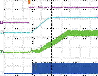


10 TYPICAL PERFORMANCE CHARACTERISTICS (continued) V IN = 12V, V OUT = 3.3V, L = 10µH, R BST =20Ω, T A = +25 C, unless otherwise noted. MPQ4420 Rev


11 TYPICAL PERFORMANCE CHARACTERISTICS (continued) V IN = 12V, V OUT = 3.3V, L = 10µH, R BST =20Ω, T A = +25 C, unless otherwise noted. MPQ4420 Rev

12 TYPICAL PERFORMANCE CHARACTERISTICS (continued) V IN = 12V, V OUT = 3.3V, L = 10µH, R BST =20Ω, T A = +25 C, unless otherwise noted. MPQ4420 Rev
13 BLOCK DIAGRAM Figure 1: Functional Block Diagram MPQ4420 Rev
14 OPERATION The MPQ4420 is a high-frequency, synchronous, rectified, step-down, switch-mode converter with built-in power MOSFETs. It offers a very compact solution to achieve 2A continuous output current with excellent load and line regulation over a wide input supply range. The MPQ4420 operates in a fixed-frequency, peak-current control mode to regulate the output voltage. An internal clock initiates a PWM cycle. The integrated high-side power MOSFET turns on and remains on until its current reaches the value set by the COMP voltage. When the power switch is off, it remains off until the next clock cycle starts. If the current in the power MOSFET does not reach the current value set by COMP within 95% of one PWM period, the power MOSFET will be forced to turn off. Internal Regulator The 5V internal regulator power most of the internal circuitries. This regulator takes the V IN input and operates in the full V IN range: When V IN exceeds 5.0V, the output of the regulator is in full regulation; when V IN falls below 5.0V, the output of the regulator decreases following the VIN. A 0.1uF decoupling ceramic capacitor is needed at the pin. Error Amplifier The error amplifier compares the FB pin voltage against the internal 0.8V reference (REF) and outputs a COMP voltage this COMP voltage controls the power MOSFET current. The optimized internal compensation network minimizes the external component count and simplifies the control loop design. Enable/SYNC Control EN/SYNC is a digital control pin that turns the regulator on and off: Drive EN high to turn on the regulator, drive it low to turn it off. An internal 500kΩ resistor from EN/SYNC to GND allows EN/SYNC to be floated to shut down the chip. The EN pin is clamped internally using a 6.5V series Zener diode, as shown in Figure 2. Connect the EN input pin through a pullup resistor to any voltage connected to the V IN pin the pullup resistor limits the EN input current to less than 150µA. For example, with 12V connected to V IN, R PULLUP (12V 6.5V) 150µA = 36.7kΩ. Connecting the EN pin directly to a voltage source without any pullup resistor requires limiting voltage amplitude to 6V to prevent damage to the Zener diode. Figure 2: 6.5V-type Zener Diode Connect an external clock with a range of 200kHz to 2.2MHz 2ms after output voltage is set to synchronize the internal clock rising edge to the external clock rising edge. The pulse width of external clock signal should be less than 1.7μs. Under-Voltage Lockout Under-voltage lockout (UVLO) protects the chip from operating at an insufficient supply voltage. The MPQ4420 UVLO comparator monitors the output voltage of the internal regulator, VCC. The UVLO rising threshold is about 3.5V while its falling threshold is 3.3V. Internal Soft-Start The soft-start prevents the converter output voltage from overshooting during startup. When the chip starts, the internal circuitry generates a soft-start voltage (SS) that ramps up from 0V to 1.2V. When SS is lower than REF, SS overrides REF so the error amplifier uses SS as the reference. When SS exceeds REF, the error amplifier uses REF as the reference. The SS time is internally set to 1.5ms. Over-Current Protection and Hiccup The MPQ4420 has cycle-by-cycle over current limit when the inductor current peak value exceeds the set current limit threshold. If the output voltage starts to drop until FB is below the Under-Voltage (UV) threshold typically 84% below the reference the MPQ4420 enters hiccup mode to periodically restart the part. This protection mode is especially useful when the output is dead-shorted to ground. The average short-circuit current is greatly reduced to alleviate the thermal issue and to protect the regulator. MPQ4420 Rev
15 The MPQ4420 exits the hiccup mode once the over-current condition is removed. Thermal Shutdown Thermal shutdown prevents the chip from operating at exceedingly high temperatures. When the silicon die temperature exceeds 170 C, it shuts down the whole chip. When the temperature drops below its lower threshold (typically 140 C) the chip is enabled again. Floating Driver and Bootstrap Charging An external bootstrap capacitor power the floating-power-mosfet driver. A dedicated internal regulator (see figure 3) charges and regulates the bootstrap capacitor voltage to ~5V. When the voltage between the BST and SW nodes drops below regulation, a PMOS pass transistor connected from V IN to BST turns on. The charging current path is from V IN, BST and then to SW. The external circuit should provide enough voltage headroom to facilitate charging. As long as V IN is significantly higher than SW, the bootstrap capacitor remains charged. When the HS-FET is ON, V IN V SW so the bootstrap capacitor cannot charge. When the LS-FET is ON, V IN V SW reaches its maximum for fast charging. When there is no inductor current, V SW =V OUT so the difference between V IN and V OUT can charge the bootstrap capacitor. The floating driver has its own UVLO protection, with a rising threshold of 2.2V and hysteresis of 150mV. A 20Ω resistor placed between SW and BST cap is strongly recommended to reduce SW spike voltage. Startup and Shutdown If both V IN and EN exceed their appropriate thresholds, the chip starts: The reference block starts first, generating stable reference voltage and currents, and then the internal regulator is enabled. The regulator provides stable supply for the remaining circuitries. Three events can shut down the chip: EN low, V IN low, and thermal shutdown. In the shutdown procedure, the signaling path is first blocked to avoid any fault triggering. The COMP voltage and the internal supply rail are then pulled down. The floating driver is not subject to this shutdown command. Power Good The MPQ4420 has power good (PG) output. The PG pin is the open drain of a MOSFET. It should be connected to VCC or some other voltage source through a resistor (e.g. 100kΩ). In the presence of an input voltage, the MOSFET turns on so that the PG pin is pulled to low before SS is ready. After V FB reaches 90% REF, the PG pin is pulled high after a delay, typically 90μs. When V FB drops to 84% REF, the PG pin is pulled low. Also, PG is pulled low if thermal shutdown or EN is pulled low. Figure 3: Internal Bootstrap Charging Circuit MPQ4420 Rev
16 APPLICATION INFORMATION Setting the Output Voltage The external resistor divider sets the output voltage (see Typical Application on page 1). The feedback resistor R1 also sets the feedback loop bandwidth with the internal compensation capacitor. Choose R1 around 40kΩ. R2 is then given by: R2 = R1 VOUT V The T-type network as shown in Figure 4 is highly recommended when V OUT is low. Choose the inductor ripple current to be approximately 30% of the maximum load current. The maximum inductor peak current is: ΔIL IL(MAX) = ILOAD + 2 Use a larger inductor for improved efficiency under light-load conditions below 100mA. VIN UVLO Setting MPQ4420 has internal fix under voltage lock out (UVLO) threshold: rising threshold is 3.5V while falling threshold is about 3.3V. For the application needs higher UVLO point, external resistor divider between EN and IN as shown in figure 4 can be used to get higher equivalent UVLO threshold. Figure 4: T-Type Network RT+R1 is used to set the loop bandwidth. Basically, higher RT+R1, lower bandwidth. To ensure the loop stability, it is strongly recommended to limit the bandwidth lower than 40kHz based on the 410kHz default fsw. Table 1 lists the recommended T-type resistors value for common output voltages. Table 1: Resistor Selection for Common Output Voltages V OUT (V) R1 (kω) R2 (kω) RT (kω) (1%) 13 (1%) 51 (1%) (1%) 7.68 (1%) 51 (1%) Selecting the Inductor Use a1µh-to-10µh inductor with a DC current rating of at least 25% percent higher than the maximum load current for most applications. For highest efficiency, an inductor with small DC resistance is recommended. For most designs, the inductance value can be derived from the following equation. V OUT (VIN V OUT ) L1 = VIN Δ IL fosc Where ΔI L is the inductor ripple current. VIN R5 R6 IN EN 500k Figure 5: Adjustable UVLO using EN divider The UVLO threshold can be computed from below two equations: R5 INUV = (1+ ) 500k//R6 RISING V EN_RISING R5 INUV = (1+ ) 500k//R6 Where V EN_RISING =1.4V, V EN_FALLING =1.25V. FALLING V EN_FALLING When choose R5, make sure it is big enough to limit the current flows into EN pin lower than 150uA. MPQ4420 Rev
17 Selecting the Input Capacitor The input current to the step-down converter is discontinuous, therefore requires a capacitor is to supply the AC current to the step-down converter while maintaining the DC input voltage. Use low ESR capacitors for the best performance. Use ceramic capacitors with X5R or X7R dielectrics for best results because of their low ESR and small temperature coefficients. For most application, a 22µF ceramic capacitor is sufficient to maintain the DC input voltage. And it is strongly recommended to use another lower value capacitor (e.g. 0.1µF) with small package size (0603) to absorb high frequency switching noise. Make sure place the small size capacitor as close to IN and GND pins as possible (see PCB LAYOUT section). Since C1 absorbs the input switching current, it requires an adequate ripple current rating. The RMS current in the input capacitor can be estimated by: I C1 = I LOAD V V OUT 1 IN V V OUT IN The worse case condition occurs at V IN = 2V OUT, where: ILOAD IC 1 = 2 For simplification, choose an input capacitor with an RMS current rating greater than half of the maximum load current. The input capacitor can be electrolytic, tantalum or ceramic. When using electrolytic or tantalum capacitors, add a small, high quality ceramic capacitor (e.g. 1μF) placed as close to the IC as possible. When using ceramic capacitors, make sure that they have enough capacitance to provide sufficient charge to prevent excessive voltage ripple at input. The input voltage ripple caused by capacitance can be estimated by: ILOAD V OUT V OUT Δ VIN = 1 fs C1 VIN VIN Selecting the Output Capacitor The output capacitor (C2) maintains the DC output voltage. Use ceramic, tantalum, or low- ESR electrolytic capacitors. For best results, use low ESR capacitors to keep the output voltage ripple low. The output voltage ripple can be estimated by: V OUT V OUT 1 Δ VOUT = 1 RESR + fs L1 VIN 8 fs C2 Where L 1 is the inductor value and R ESR is the equivalent series resistance (ESR) value of the output capacitor. For ceramic capacitors, the capacitance dominates the impedance at the switching frequency, and the capacitance causes the majority of the output voltage ripple. For simplification, the output voltage ripple can be estimated by: V V ΔV = 1 OUT OUT OUT 2 8 fs L1 C2 VIN For tantalum or electrolytic capacitors, the ESR dominates the impedance at the switching frequency. For simplification, the output ripple can be approximated to: V OUT OUT ΔVOUT = 1 RESR fs L 1 V IN The characteristics of the output capacitor also affect the stability of the regulation system. The MPQ4420 can be optimized for a wide range of capacitance and ESR values. V MPQ4420 Rev
18 BST Resistor and External BST Diode A 20ohm resistor in series with BST capacitor is recommended to reduce the SW spike voltage. Higher resistance is better for SW spike reduction, but will compromise the efficiency on the other hand. An external BST diode can enhance the efficiency of the regulator when the duty cycle is high (>65%). A power supply between 2.5V and 5V can be used to power the external bootstrap diode and VCC or VOUT is the good choice of this power supply in the circuit as shown in Figure 6. 3) Use large ground plane directly connect to GND pin. Add vias near the GND pin if bottom layer is ground plane. 4) Route SW, BST away from sensitive analog areas such as FB. 5) Place the T-type feedback resistor close to chip to ensure the trace which connects to FB pin as the short as possible. VCC 7 BST 5 External BST diode 1N4148 R BST VCC/V OUT SW 3 C BST L C OUT V OUT Figure 6: Optional External Bootstrap Diode to Enhance Efficiency The recommended external BST diode is IN4148, and the BST capacitor value is 0.1µF to 1μF. PCB Layout PCB layout, especially the input capacitor and VCC capacitor placement, is very important to achieve stable operation. For the best results, follow these guidelines: 1) Place the ceramics input capacitor as close to IN and GND pins as possible, especially the small package size (0603) input bypass capacitor. Keep the connection of input capacitor and IN pin as short and wide as possible. 2) Place the VCC capacitor to VCC pin and GND pin as close as possible. Make the trace length of VCC pin-vcc capacitor anode-vcc capacitor cathode-chip GND pin as short as possible. Top Layer Bottom Layer Figure 7: Recommended PCB Layout MPQ4420 Rev
19 TYPICAL APPLICATION CIRCUITS Figure 8: 3.3V Output Typical Application Circuit MPQ4420 Rev
20 PACKAGE INFORMATION TSOT23-8 TOP VIEW RECOMMENDED LAND PATTERN SEATING PLANE SEE DETAIL A FRONT VIEW SIDE VIEW NOTE: DETAIL A 1) ALL DIMENSIONS ARE IN MILLIMETERS. 2) PACKAGE LENGTH DOES NOT INCLUDE MOLD FLASH, PROTRUSION OR GATE BURR. 3) PACKAGE WIDTH DOES NOT INCLUDE INTERLEAD FLASH OR PROTRUSION. 4) LEAD COPLANARITY (BOTTOM OF LEADS AFTER FORMING) SHALL BE 0.10 MILLIMETERS MAX. 5) JEDEC REFERENCE IS MO-193, VARIATION BA. 6) DRAWING IS NOT TO SCALE. NOTICE: The information in this document is subject to change without notice. Users should warrant and guarantee that third party Intellectual Property rights are not infringed upon when integrating MPS products into any application. MPS will not assume any legal responsibility for any said applications. MPQ4420 Rev
MP2259 1A, 16V, 1.4MHz Step-Down Converter
 MP59 1A, 1V, 1.MHz Step-Down Converter TM The Future of Analog IC Technology DESCRIPTION The MP59 is a monolithic integrated stepdown switch mode converter with an internal power MOSFET. It achieves 1A
MP2456 0.5A, 50V, 1.2MHz Step-Down Converter in a TSOT23-6
 MP2456 0.5A, 50V, 1.2MHz Step-Down Converter in a TSOT23-6 DESCRIPTION The MP2456 is a monolithic, step-down, switchmode converter with a built-in power MOSFET. It achieves a 0.5A peak-output current over
MP2365 3A, 28V, 1.4MHz Step-Down Converter
 The Future of Analog IC Technology MP365 3A, 8,.MHz Step-Down Converter DESCRIPTION The MP365 is a.mhz step-down regulator with a built-in Power MOSFET. It achieves 3A continuous output current over a
TM MP2305 2A, 23V SYNCHRONOUS RECTIFIED, STEP-DOWN CONVERTER
 The Future of Analog IC Technology TM TM MP305 A, 3 Synchronous Rectified Step-Down Converter DESCRIPTION The MP305 is a monolithic synchronous buck regulator. The device integrates 30mΩ MOSFETS that provide
MP1541 1.3MHz Boost Converter
 MP5.3MHz Boost Converter The Future of Analog IC Technology DESCRIPTION The MP5 is a 5-pin thin SOT3 current mode step up converter intended for small, low power applications. The MP5 switches at.3mhz
LDS8720. 184 WLED Matrix Driver with Boost Converter FEATURES APPLICATION DESCRIPTION TYPICAL APPLICATION CIRCUIT
 184 WLED Matrix Driver with Boost Converter FEATURES High efficiency boost converter with the input voltage range from 2.7 to 5.5 V No external Schottky Required (Internal synchronous rectifier) 250 mv
28V, 2A Buck Constant Current Switching Regulator for White LED
 28V, 2A Buck Constant Current Switching Regulator for White LED FP7102 General Description The FP7102 is a PWM control buck converter designed to provide a simple, high efficiency solution for driving
MPM3810. 6V Input, 1.2A Module Synchronous Step-Down Converter with Integrated Inductor DESCRIPTION FEATURES APPLICATIONS
 The Future of Analog IC Technology MPM3810 6 Input, 1.2A Module Synchronous Step-Down Converter with Integrated Inductor DESCRIPTION The MPM3810 is a step-down module converter with built-in power MOSFETs
Datasheet. 2A 380KHZ 20V PWM Buck DC/DC Converter. Features
 General Description Features The is a 380 KHz fixed frequency monolithic step down switch mode regulator with a built in internal Power MOSFET. It achieves 2A continuous output current over a wide input
LM5001 High Voltage Switch Mode Regulator
 High Voltage Switch Mode Regulator General Description The LM5001 high voltage switch mode regulator features all of the functions necessary to implement efficient high voltage Boost, Flyback, SEPIC and
AAT4280 Slew Rate Controlled Load Switch
 General Description Features SmartSwitch The AAT4280 SmartSwitch is a P-channel MOSFET power switch designed for high-side load switching applications. The P-channel MOSFET device has a typical R DS(ON)
MP1493 3A, 4.2V-16V Input, Fast Transient Synchronous Step-down Converter
 The Future of Analog IC Technology DESCRIPTION The MP493 is a fully integrated, high efficiency 3A synchronous rectified step-down converter. The MP493 operates at high efficiency over a wide output current
FAN5346 Series Boost LED Driver with PWM Dimming Interface
 FAN5346 Series Boost LED Driver with PWM Dimming Interface Features Asynchronous Boost Converter Drives LEDs in Series: FAN5346S20X: 20V Output FAN5346S30X: 30V Output 2.5V to 5.5V Input Voltage Range
CAT4101TV. 1 A Constant-Current LED Driver with PWM Dimming
 A Constant-Current LED Driver with PWM Dimming Description The CAT4 is a constant current sink driving a string of high brightness LEDs up to A with very low dropout of.5 V at full load. It requires no
PAM2804. Pin Assignments. Description. Applications. Features. Typical Applications Circuit 1A STEP-DOWN CONSTANT CURRENT, HIGH EFFICIENCY LED DRIVER
 1A STEP-DOWN CONSTANT CURRENT, HIGH EFFICIENCY LED DRIER Description Pin Assignments The is a step-down constant current LED driver. When the input voltage is down to lower than LED forward voltage, then
CAT4139. 22 V High Current Boost White LED Driver
 22 V High Current Boost White LED Driver Description The CAT4139 is a DC/DC step up converter that delivers an accurate constant current ideal for driving LEDs. Operation at a fixed switching frequency
TYPICAL APPLICATION CIRCUIT. ORDER INFORMATION SOP-EP 8 pin A703EFT (Lead Free) A703EGT (Green)
 A703EGT (Green)") www.addmtek.com 2 CHANNELS 150mA HIGH VOLTAGE ADJUSTABLE CURRENT REGULATOR DESCRIPTION A703 is a high voltage, adjustable constant current driver for LED applications. Two regulated current ports are designed
www.addmtek.com 2 CHANNELS 150mA HIGH VOLTAGE ADJUSTABLE CURRENT REGULATOR DESCRIPTION A703 is a high voltage, adjustable constant current driver for LED applications. Two regulated current ports are designed
AP1509. 150KHz, 2A PWM BUCK DC/DC CONVERTER. Description. Pin Assignments V IN. Applications. Features. (Top View) GND GND. Output AP1509 GND GND
 GND GND. Output AP1509 GND GND") Description Pin Assignments The series are monolithic IC designed for a stepdown DC/DC converter, and own the ability of driving a 2A load without additional transistor. It saves board space. The external
Description Pin Assignments The series are monolithic IC designed for a stepdown DC/DC converter, and own the ability of driving a 2A load without additional transistor. It saves board space. The external
AP1510. General Description. Features. Applications. Typical Application Circuit PWM CONTROL 3A STEP-DOWN CONVERTER AP1510. x (1+R A = V FB /R B
 Features General Description Input voltage: 3.6 to 23 Output voltage: 0.8 to CC. Duty ratio: 0% to 100% PWM control Oscillation frequency: 300kHz typ. Current Limit, Enable function Thermal Shutdown function
MIC33050. General Description. Features. Applications. Typical Application. 4MHz Internal Inductor PWM Buck Regulator with HyperLight Load
 4MHz Internal Inductor PWM Buck Regulator with HyperLight Load General Description The Micrel is a high-efficiency 600mA PWM synchronous buck (step-down) regulator with internal inductor featuring HyperLight
ST1S10. 3 A, 900 khz, monolithic synchronous step-down regulator. Features. Description. Applications
 3 A, 900 khz, monolithic synchronous step-down regulator Features Step-down current mode PWM regulator Output voltage adjustable from 0.8 V Input voltage from 2.5 V up to 18 V 2% DC output voltage tolerance
LD7550-B. Green-Mode PWM Controller. General Description. Features. Applications. Typical Application. REV: 01a 12/22/2006 LD7550-B
 12/22/2006 REV: 01a Green-Mode PWM Controller General Description The LD7550-B is a low cost, low startup current, current mode PWM controller with green-mode power-saving operation. The integrated functions
ICS650-44 SPREAD SPECTRUM CLOCK SYNTHESIZER. Description. Features. Block Diagram DATASHEET
 DATASHEET ICS650-44 Description The ICS650-44 is a spread spectrum clock synthesizer intended for video projector and digital TV applications. It generates three copies of an EMI optimized 50 MHz clock
UNISONIC TECHNOLOGIES CO., LTD
 UPS61 UNISONIC TECHNOLOGIES CO., LTD HIGH PERFORMANCE CURRENT MODE POWER SWITCH DESCRIPTION The UTC UPS61 is designed to provide several special enhancements to satisfy the needs, for example, Power-Saving
Push-Pull FET Driver with Integrated Oscillator and Clock Output
 19-3662; Rev 1; 5/7 Push-Pull FET Driver with Integrated Oscillator General Description The is a +4.5V to +15V push-pull, current-fed topology driver subsystem with an integrated oscillator for use in
LM1084 5A Low Dropout Positive Regulators
 5A Low Dropout Positive Regulators General Description The LM1084 is a series of low dropout voltage positive regulators with a maximum dropout of 1.5 at 5A of load current. It has the same pin-out as
LM2704 Micropower Step-up DC/DC Converter with 550mA Peak Current Limit
 Micropower Step-up DC/DC Converter with 550mA Peak Current Limit General Description The LM2704 is a micropower step-up DC/DC in a small 5-lead SOT-23 package. A current limited, fixed off-time control
29V High Voltage LED Driver
 29V High Voltage LED Driver SP7601 FEATURES Wide Input Voltage Range 4.5V 29V 1.2MHz Constant Frequency Operation Low 0.2V Reference Voltage Adjustable Overcurrent Protection PWM Dimming and Power sequencing
Series AMLDL-Z Up to 1000mA LED Driver
 FEATURES: Click on Series name for product info on aimtec.com Series Up to ma LED Driver Models Single output Model Input Voltage (V) Step Down DC/DC LED driver Operating Temperature range 4ºC to 85ºC
L6384E. High voltage half-bridge driver. Description. Features. Applications
 High voltage half-bridge driver Description Datasheet - production data Features High voltage rail up to 600 V dv/dt immunity ± 50 V/nsec in full temperature range Driver current capability 400 ma source
28 V, 56 m, Load Switch with Programmable Current Limit and Slew Rate Control
 28 V, 56 m, Load Switch with Programmable Current Limit and Slew Rate Control OPERATION DESCRIPTION SiP32419 and SiP32429 are load switches that integrate multiple control features that simplify the design
LM138 LM338 5-Amp Adjustable Regulators
 LM138 LM338 5-Amp Adjustable Regulators General Description The LM138 series of adjustable 3-terminal positive voltage regulators is capable of supplying in excess of 5A over a 1 2V to 32V output range
SG2525A SG3525A REGULATING PULSE WIDTH MODULATORS
 SG2525A SG3525A REGULATING PULSE WIDTH MODULATORS 8 TO 35 V OPERATION 5.1 V REFERENCE TRIMMED TO ± 1 % 100 Hz TO 500 KHz OSCILLATOR RANGE SEPARATE OSCILLATOR SYNC TERMINAL ADJUSTABLE DEADTIME CONTROL INTERNAL
400KHz 60V 4A Switching Current Boost / Buck-Boost / Inverting DC/DC Converter
 Features Wide 5V to 32V Input Voltage Range Positive or Negative Output Voltage Programming with a Single Feedback Pin Current Mode Control Provides Excellent Transient Response 1.25V reference adjustable
LTC3026 1.5A Low Input Voltage VLDO Linear Regulator. Description. Features. Applications. Typical Application
 Features n Input Voltage Range: 1.14V to 3.5V (with Boost Enabled) 1.14V to 5.5V (with External 5V Boost) n Low Dropout Voltage: 1mV at I = 1.5A n Adjustable Output Range:.4V to 2.6V n Output Current:
Preliminary Datasheet
 Features Macroblock Preliminary Datasheet 1.2A Constant Output Current 93% Efficiency @ input voltage 13V, 350mA, 9~36V Input Voltage Range Hysteretic PFM Improves Efficiency at Light Loads Settable Output
Cool-Power PI33xx-x0. 8 V to 36 V IN Cool-Power ZVS Buck Regulator Family. Product Description. Features & Benefits. Applications. Package Information
 Cool-Power PI33xx-x0 8 V to 36 V IN Cool-Power ZVS Buck Regulator Family Product Description The PI33xx-x0 is a family of high efficiency, wide input range DC-DC ZVS-Buck regulators integrating controller,
TDA4605 CONTROL CIRCUIT FOR SWITCH MODE POWER SUPPLIES USING MOS TRANSISTORS
 CONTROL CIRCUIT FOR SWITCH MODE POWER SUPPLIES USING MOS TRANSISTORS Fold-Back Characteristic provides Overload Protection for External Diodes Burst Operation under Short-Circuit and no Load Conditions
AP1506. 150KHz, 3A PWM BUCK DC/DC CONVERTER. Pin Assignments. Description. Features. Applications. ( Top View ) 5 SD 4 FB 3 Gnd 2 Output 1 V IN
 5 SD 4 FB 3 Gnd 2 Output 1 V IN") Description Pin Assignments The series are monolithic IC designed for a stepdown DC/DC converter, and own the ability of driving a 3A load without external transistor. Due to reducing the number of external
Description Pin Assignments The series are monolithic IC designed for a stepdown DC/DC converter, and own the ability of driving a 3A load without external transistor. Due to reducing the number of external
SC339. Ultra Low Output Voltage Linear FET Controller POWER MANAGEMENT. Applications. Typical Application Circuit
 Description The SC339 is an ultra-low output voltage, linear power supply controller designed to simplify power management for notebook PCs. It is part of Semtech s Smart LDO TM family of products. The
ICS514 LOCO PLL CLOCK GENERATOR. Description. Features. Block Diagram DATASHEET
 DATASHEET ICS514 Description The ICS514 LOCO TM is the most cost effective way to generate a high-quality, high-frequency clock output from a 14.31818 MHz crystal or clock input. The name LOCO stands for
1ED Compact A new high performance, cost efficient, high voltage gate driver IC family
 1ED Compact A new high performance, cost efficient, high voltage gate driver IC family Heiko Rettinger, Infineon Technologies AG, Am Campeon 1-12, 85579 Neubiberg, Germany, heiko.rettinger@infineon.com
5.5 V Input, 300 ma, Low Quiescent Current, CMOS Linear Regulator ADP122/ADP123
 Data Sheet 5.5 V Input, 3 ma, Low Quiescent Current, CMOS Linear Regulator ADP/ADP3 FEATURES Input voltage supply range:.3 V to 5.5 V 3 ma maximum output current Fixed and adjustable output voltage versions
PAM2316. Description. Pin Assignments. Applications. Features. A Product Line of. Diodes Incorporated. 2.5MHz, FAST TRANSIENT 2A STEP-DOWN CONVERTER
 2.5MHz, FAST TRANSIENT 2A STEP-DOWN CONVERTER Description Pin Assignments The is a 2A step-down sync converter. The 2.5MHz switching frequency enables the use of small external components. The ultra-small
CAT4109, CAV4109. 3-Channel Constant-Current RGB LED Driver with Individual PWM Dimming
 3-Channel Constant-Current RGB LED Driver with Individual PWM Dimming Description The CAT419/CAV419 is a 3 channel constant current LED driver, requiring no inductor. LED channel currents up to 175 ma
IR1168S DUAL SMART RECTIFIER DRIVER IC
 Datasheet No PD97382 September 26, 2011 IR1168S DUAL SMART RECTIFIER DRIVER IC Features Secondary-side high speed controller for synchronous rectification in resonant half bridge topologies 200V proprietary
Enpirion Power Datasheet EP53F8QI 1500 ma PowerSoC Voltage Mode Synchronous PWM Buck with Integrated Inductor
 Enpirion Power Datasheet EP53F8QI 1500 ma PowerSoC Voltage Mode Synchronous PWM Buck with Integrated Inductor Description The EP53F8QI provides high efficiency in a very small footprint. Featuring integrated
IS31LT3360 40V/1.2A LED DRIVER WITH INTERNAL SWITCH. January 2014
 40V/1.2A LED DRIVER WITH INTERNAL SWITCH January 2014 GENERAL DESCRIPTION The IS31LT3360 is a continuous mode inductive step-down converter, designed for driving a single LED or multiple series connected
NCP707. 200 ma, Very-Low Quiescent Current, I Q 25 A, Low Noise, Low Dropout Regulator
 NCP77 2 ma, Very-Low Quiescent Current, I Q 25 A, Low Noise, Low Dropout Regulator The NCP77 is 2 ma LDO that provides the engineer with a very stable, accurate voltage with very low noise suitable for
WHITE LED STEP-UP CONVERTER. Features
 General Description The is an inductor-based DC/DC converter designed to drive up to eight white LEDs in series for backlight. Only one feedback resistor is needed to control the LED current and obtain
NCT3941S/S-A Nuvoton 4 Times Linear Fan Driver NCT3941S/S-A
 Nuvoton 4 Times Linear Fan Driver NCT3941S/S-A -I- Revision A4 Table of Content- 1. GENERAL DESCRIPTION...1 2. FEATURES...1 3. APPLICATION...1 4. BLOCK DIAGRAM...2 5. PIN CONFIGURATION AND TYPICAL APPLICATION
AS2815. 1.5A Low Dropout Voltage Regulator Adjustable & Fixed Output, Fast Response
 1.5A Low Dropout oltage Regulator Adjustable & Fixed Output, Fast Response FEATURES Adjustable Output Down To 1.2 Fixed Output oltages 1.5, 2.5, 3.3, 5.0 Output Current of 1.5A Low Dropout oltage 1.1 Typ.
LM2576R. 3.0A, 52kHz, Step-Down Switching Regulator FEATURES. Applications DESCRIPTION TO-220 PKG TO-220V PKG TO-263 PKG ORDERING INFORMATION
 LM2576 FEATURES 3.3, 5.0, 12, 15, and Adjustable Output ersions Adjustable ersion Output oltage Range, 1.23 to 37 +/- 4% AG10Maximum Over Line and Load Conditions Guaranteed 3.0A Output Current Wide Input
Pulse Width Modulation Amplifiers EQUIVALENT CIRCUIT DIAGRAM. 200mV + - SMART CONTROLLER .01F OSC Q3. 2200pF
 Pulse Width Modulation Amplifiers MSA MSA FEATURES LOW COST HIGH VOLTAGE VOLTS HIGH OUTPUT CURRENT AMPS kw OUTPUT CAPABILITY VARIABLE SWITCHING FREQUEY APPLICATIONS BRUSH MOTOR CONTROL MRI MAGNETIC BEARINGS
1 TO 4 CLOCK BUFFER ICS551. Description. Features. Block Diagram DATASHEET
 DATASHEET 1 TO 4 CLOCK BUFFER ICS551 Description The ICS551 is a low cost, high-speed single input to four output clock buffer. Part of IDT s ClockBlocks TM family, this is our lowest cost, small clock
L4970A 10A SWITCHING REGULATOR
 10A SWITCHING REGULATOR 10A OUTPUT CURRENT 5.1 TO 40 OUTPUT OLTAGE RANGE 0 TO 90% DUTY CYCLE RANGE INTERNAL FEED-FORWARD LINE REGULA- TION INTERNAL CURRENT LIMITING PRECISE 5.1 ± 2% ON CHIP REFERENCE RESET
1.5A Very L.D.O Voltage Regulator LM29150/29151/29152
 FEATURES High Current Capability 1.5A Low Dropout Voltage 350mV Low Ground Current Accurate 1% Guaranteed Initial Tolerance Extremely Fast Transient Response Reverse-Battery and "Load Dump" Protection
3-Channel Supervisor IC for Power Supply
 3-Channel Supervisor IC for Power Supply Features Over-voltage protection and lockout Under-voltage protection and lockout Open drain power good output signal Built-in 300mS delay for power good 38mS de-bounce
1.5A ASYNCHRONOUS DC-DC BUCK CONV
 General Description The is a 1.4MHz fixed frequency, current mode, PWM buck (step-down) DC-DC converter, capable of driving a 1.5A load with high efficiency, excellent line and load regulation. The device
ICS650-01 SYSTEM PERIPHERAL CLOCK SOURCE. Description. Features. Block Diagram DATASHEET
 DATASHEET ICS650-01 Description The ICS650-01 is a low-cost, low-jitter, high-performance clock synthesizer for system peripheral applications. Using analog/digital Phase-Locked Loop (PLL) techniques,
www.jameco.com 1-800-831-4242
 Distributed by: www.jameco.com 1-800-831-4242 The content and copyrights of the attached material are the property of its owner. LP3961/LP3964 800mA Fast Ultra Low Dropout Linear Regulators General Description
TRIPLE PLL FIELD PROG. SPREAD SPECTRUM CLOCK SYNTHESIZER. Features
 DATASHEET ICS280 Description The ICS280 field programmable spread spectrum clock synthesizer generates up to four high-quality, high-frequency clock outputs including multiple reference clocks from a low-frequency
AAT1150 1MHz 1A Step-Down DC/DC Converter
 General Description Features SwitchReg The AAT115 SwitchReg is a step-down switching converter ideal for applications where high efficiency, small size, and low ripple are critical. Able to deliver 1A
High Accuracy, Ultralow IQ, 1.5 A, anycap Low Dropout Regulator ADP3339
 Data Sheet High Accuracy, Ultralow IQ,.5 A, anycap Low Dropout Regulator FEATURES FUNCTIONAL BLOCK DIAGRAM High accuracy over line and load: ±.9% at 5 C, ±.5% over temperature Ultralow dropout voltage:
DDR SDRAM Memory Termination USING THE LX1672 AND LX1673 FOR DDR SDRAM MEMORY TERMINATION INTEGRATED PRODUCTS. Microsemi
 AN-17 USING THE LX1672 AND LX1673 FOR DDR SDRAM MEMORY TERMINATION LX1672 Protected by US Patents: 6,285,571 & 6,292,378 INTEGRATED PRODUCTS Page 1 TABLE OF CONTENTS 1.0 INTRODUCTION... 3 2.0 SDR vs DDR
STCS1A. 1.5 A max constant current LED driver. Features. Applications. Description
 1.5 A max constant current LED driver Features Up to 40 V input voltage Less than 0.5 V voltage overhead Up to 1.5 A output current PWM dimming pin Shutdown pin LED disconnection diagnostic DFN8 (3 x 3
ICS379. Quad PLL with VCXO Quick Turn Clock. Description. Features. Block Diagram
 Quad PLL with VCXO Quick Turn Clock Description The ICS379 QTClock TM generates up to 9 high quality, high frequency clock outputs including a reference from a low frequency pullable crystal. It is designed
AAT3238 DATA SHEET. 300mA MicroPower TM High Performance LDO Linear Regulator. Applications. Features. General Description. Typical Application
 General Description The MicroPower low dropout (LDO) linear regulator is ideally suited for portable applications where very fast transient response, extended battery life, and small size are critical.
Features. 3.3V,100mA 0.85V. COUT 4.7μF. Skyworks Solutions, Inc. Phone [781] 376-3000 Fax [781] 376-3100 sales@skyworksinc.com www.skyworksinc.
![Features. 3.3V,100mA 0.85V. COUT 4.7μF. Skyworks Solutions, Inc. Phone [781] 376-3000 Fax [781] 376-3100 sales@skyworksinc.com www.skyworksinc.](/thumbs/39/19150322.jpg "Features. 3.3V,100mA 0.85V. COUT 4.7μF. Skyworks Solutions, Inc. Phone [781] 376-3000 Fax [781] 376-3100 sales@skyworksinc.com www.skyworksinc.") General Description The is a high efficiency, synchronous, fixed frequency, step-up converter designed for single-cell or dual-cell alkaline, NiMH, or NiCd battery-powered applications. The high 1.2MHz
General Description The is a high efficiency, synchronous, fixed frequency, step-up converter designed for single-cell or dual-cell alkaline, NiMH, or NiCd battery-powered applications. The high 1.2MHz
LM117 LM317A LM317 3-Terminal Adjustable Regulator
 LM117 LM317A LM317 3-Terminal Adjustable Regulator General Description The LM117 series of adjustable 3-terminal positive voltage regulators is capable of supplying in excess of 1 5A over a 1 2V to 37V
NCP1529. 1.7MHz, 1A, High Efficiency, Low Ripple, Adjustable Output Voltage Step-down Converter
 .7MHz, A, High Efficiency, Low Ripple, Adjustable Output Voltage Step-down Converter The NCP529 stepdown DCDC converter is a monolithic integrated circuit for portable applications powered from one cell
UC3842/UC3843/UC3844/UC3845
 SMPS Controller www.fairchildsemi.com Features Low Start up Current Maximum Duty Clamp UVLO With Hysteresis Operating Frequency up to 500KHz Description The UC3842/UC3843/UC3844/UC3845 are fixed frequencycurrent-mode
SPREAD SPECTRUM CLOCK GENERATOR. Features
 DATASHEET ICS7152 Description The ICS7152-01, -02, -11, and -12 are clock generators for EMI (Electro Magnetic Interference) reduction (see below for frequency ranges and multiplier ratios). Spectral peaks
Advanced Monolithic Systems
 Advanced Monolithic Systems FEATURES Three Terminal Adjustable or Fixed oltages* 1.5, 1.8, 2.5, 2.85, 3.3 and 5. Output Current of 1A Operates Down to 1 Dropout Line Regulation:.2% Max. Load Regulation:.4%
High Accuracy, Ultralow IQ, 1 A, anycap Low Dropout Regulator ADP3338
 High Accuracy, Ultralow IQ, 1 A, anycap Low Dropout Regulator ADP3338 FEATURES High accuracy over line and load: ±.8% @ 25 C, ±1.4% over temperature Ultralow dropout voltage: 19 mv (typ) @ 1 A Requires
NCP3065, NCV3065. Up to 1.5 A Constant Current Switching Regulator for LEDs
 Up to.5 A Constant Current Switching Regulator for LEDs The NCP3065 is a monolithic switching regulator designed to deliver constant current for powering high brightness LEDs. The device has a very low
Features. Modulation Frequency (khz) VDD. PLL Clock Synthesizer with Spread Spectrum Circuitry GND
 VDD. PLL Clock Synthesizer with Spread Spectrum Circuitry GND") DATASHEET IDT5P50901/2/3/4 Description The IDT5P50901/2/3/4 is a family of 1.8V low power, spread spectrum clock generators capable of reducing EMI radiation from an input clock. Spread spectrum technique
DATASHEET IDT5P50901/2/3/4 Description The IDT5P50901/2/3/4 is a family of 1.8V low power, spread spectrum clock generators capable of reducing EMI radiation from an input clock. Spread spectrum technique
Understanding the Terms and Definitions of LDO Voltage Regulators
 Application Report SLVA79 - October 1999 Understanding the Terms and Definitions of ltage Regulators Bang S. Lee Mixed Signal Products ABSTRACT This report provides an understanding of the terms and definitions
Programmable Single-/Dual-/Triple- Tone Gong SAE 800
 Programmable Single-/Dual-/Triple- Tone Gong Preliminary Data SAE 800 Bipolar IC Features Supply voltage range 2.8 V to 18 V Few external components (no electrolytic capacitor) 1 tone, 2 tones, 3 tones
AP331A XX G - 7. Lead Free G : Green. Packaging (Note 2)
") Features General Description Wide supply Voltage range: 2.0V to 36V Single or dual supplies: ±1.0V to ±18V Very low supply current drain (0.4mA) independent of supply voltage Low input biasing current:
Features General Description Wide supply Voltage range: 2.0V to 36V Single or dual supplies: ±1.0V to ±18V Very low supply current drain (0.4mA) independent of supply voltage Low input biasing current:
PAM8403. Description. Pin Assignments. Features. Applications. Typical Applications Circuit. A Product Line of. Diodes Incorporated
 FILTERLESS 3W CLASS-D STEREO AUDIO AMPLIFIER Description Pin Assignments The is a 3W, class-d audio amplifier. It offers low THD+N, allowing it to achieve high-quality sound reproduction. The new filterless
RT9515. Linear Single Cell Li-Ion Battery Charger IC. General Description. Features. Applications. Ordering Information RT9515. Pin Configurations
 Linear Single Cell Li-Ion Battery Charger IC General Description The RT515 is a fully integrated low cost single-cell Li- Ion battery charger IC ideal for portable applications. The RT515 is capable of
SWITCH-MODE POWER SUPPLY CONTROLLER PULSE OUTPUT DC OUTPUT GROUND EXTERNAL FUNCTION SIMULATION ZERO CROSSING INPUT CONTROL EXTERNAL FUNCTION
 SWITCH-MODE POWER SUPPLY CONTROLLER. LOW START-UP CURRENT. DIRECT CONTROL OF SWITCHING TRAN- SISTOR. COLLECTOR CURRENT PROPORTIONAL TO BASE-CURRENT INPUT REERSE-GOING LINEAR OERLOAD CHARACTERISTIC CURE
.OPERATING SUPPLY VOLTAGE UP TO 46 V
 L298 DUAL FULL-BRIDGE DRIVER.OPERATING SUPPLY VOLTAGE UP TO 46 V TOTAL DC CURRENT UP TO 4 A. LOW SATURATION VOLTAGE OVERTEMPERATURE PROTECTION LOGICAL "0" INPUT VOLTAGE UP TO 1.5 V (HIGH NOISE IMMUNITY)
Rail-to-Rail, High Output Current Amplifier AD8397
 Rail-to-Rail, High Output Current Amplifier AD8397 FEATURES Dual operational amplifier Voltage feedback Wide supply range from 3 V to 24 V Rail-to-rail output Output swing to within.5 V of supply rails
MIC33030. General Description. Features. Applications. Typical Application. 8MHz 400mA Internal Inductor Buck Regulator with HyperLight Load
 8MHz 400mA Internal Inductor Buck Regulator with HyperLight Load General Description The is a high-efficiency, 8MHz, 400mA synchronous buck regulator with an internal inductor and HyperLight Load mode.
Simple PWM Boost Converter with I/O Disconnect Solves Malfunctions Caused when V OUT <V IN
 Simple PWM Boost Converter with I/O Disconnect Solves Malfunctions Caused when V OUT
Application Note AN-1138
 Application Note AN- IRS0(S) Functional Description By Jun Honda, Xiao-chang Cheng, Wenduo Liu Table of Contents Page General Description... Typical Implementation... PWM Modulator... MOSFET Selection...
NCP9001. 1.5 MHz, 600 ma, High Efficiency, Low Quiescent Current, Adjustable Output Voltage Step Down Converter
 .5 MHz, 6 ma, High Efficiency, Low Quiescent Current, Adjustable Output Voltage Step Down Converter The NCP step down PWM DC DC converter is optimized for portable applications powered from one cell Li
DATA SHEET. TDA8560Q 2 40 W/2 Ω stereo BTL car radio power amplifier with diagnostic facility INTEGRATED CIRCUITS. 1996 Jan 08
 INTEGRATED CIRCUITS DATA SHEET power amplifier with diagnostic facility Supersedes data of March 1994 File under Integrated Circuits, IC01 1996 Jan 08 FEATURES Requires very few external components High
High Frequency True PWM Dimming White LED Driver MP3304 and MP3305
 The Future of Analog IC Technology AN021 High Frequency True PWM Dimming White LED Driver MP3304 and MP3305 High Frequency True PWM Dimming White LED Driver MP3304 and MP3305 Prepared by Zhijun Ye and
ISL6700. 80V/1.25A Peak, Medium Frequency, Low Cost, Half-Bridge Driver. Features. Ordering Information. Applications. Pinouts
 ISL6700 Data Sheet FN9077.6 80V/1.25A Peak, Medium Frequency, Low Cost, Half-Bridge Driver The ISL6700 is an 80V/1.25A peak, medium frequency, low cost, half-bridge driver IC available in 8-lead SOIC and
LM1770 Low-Voltage SOT23 Synchronous Buck Controller With No External Compensation
 LM1770 Low-Voltage SOT23 Synchronous Buck Controller With No External Compensation General Description The LM1770 is an efficient synchronous buck switching controller in a tiny SOT23 package. The constant
STCS1. 1.5 A max constant current LED driver. Features. Applications. Description
 1.5 A max constant current LED driver Features Up to 40 V input voltage Less than 0.5 V voltage overhead Up to 1.5 A output current PWM dimming pin Shutdown pin LED disconnection diagnostic DFN8 (3x3 mm)
SELF-OSCILLATING HALF-BRIDGE DRIVER
 Data Sheet No. PD60029 revj I2155&(PbF) (NOTE: For new designs, we recommend I s new products I2153 and I21531) SELF-OSCILLATING HALF-BIDGE DIE Features Floating channel designed for bootstrap operation
LM350. 3.0 A, Adjustable Output, Positive Voltage Regulator THREE TERMINAL ADJUSTABLE POSITIVE VOLTAGE REGULATOR
 3. A, able Output, Positive Voltage Regulator The is an adjustable threeterminal positive voltage regulator capable of supplying in excess of 3. A over an output voltage range of 1.2 V to 33 V. This voltage
UNISONIC TECHNOLOGIES CO., LTD UC3863 LINEAR INTEGRATED CIRCUIT
 UNISONIC TECHNOLOGIES CO., LTD UC3863 LOW COST POWER-SAVING MODE PWM CONTROLLER FOR FLYBACK CONVERTERS DESCRIPTION The UC3863 is a high performance current mode PWM controller ideally suited for low standby
CA723, CA723C. Voltage Regulators Adjustable from 2V to 37V at Output Currents Up to 150mA without External Pass Transistors. Features.
 CA73, CA73C Data Sheet April 1999 File Number 788. Voltage Regulators Adjustable from V to 37V at Output Currents Up to 1mA without External Pass Transistors The CA73 and CA73C are silicon monolithic integrated
Supertex inc. HV256. 32-Channel High Voltage Amplifier Array HV256. Features. General Description. Applications. Typical Application Circuit
 32-Channel High Voltage Amplifier Array Features 32 independent high voltage amplifiers 3V operating voltage 295V output voltage 2.2V/µs typical output slew rate Adjustable output current source limit
Supply voltage Supervisor TL77xx Series. Author: Eilhard Haseloff
 Supply voltage Supervisor TL77xx Series Author: Eilhard Haseloff Literature Number: SLVAE04 March 1997 i IMPORTANT NOTICE Texas Instruments (TI) reserves the right to make changes to its products or to