Systemy RT i embedded Wykład 6 Rdzenie ARM, część 2
|
|
|
- Sabina Lamb
- 7 years ago
- Views:
Transcription

1 Systemy RT i embedded Wykład 6 Rdzenie ARM, część 2 Wrocław 2013
2 Pipelining
3 What Is A Pipeline? Pipelining is used by virtually all modern microprocessors to enhance performance by overlapping the execution of instructions. In terms of a pipeline within a CPU, each instruction is broken up into different stages.
4 What Is A Pipeline? Ideally if each stage is balanced (all stages are ready to start at the same time and take an equal amount of time to execute.) the time taken per instruction (pipelined) is defined as: Time per instruction (unpipelined) / Number of stages
5 What is a pipeline If the stages of a pipeline are not balanced and one stage is slower than another, the entire throughput of the pipeline is affected.
6 What is a pipeline In terms of a CPU, the implementation of pipelining has the effect of reducing the average instruction time, therefore reducing the average CPI (Clocks per Instruction). Example: If each instruction in a microprocessor takes 5 clock cycles (unpipelined) and we have a 4 stage pipeline, the ideal average CPI with the pipeline will be 1.25.
7 Classical 5-stage pipeline Usually we have 5 cycle deep pipeline: Instruction Fetch Cycle Instruction Decode/Register Fetch Cycle Execution Cycle Memory Access Cycle Write-Back Cycle
8 Instruction Fetch (IF) Cycle During IF cycle the instructiondecoder fetches an instruction from an instruction memory
9 Instruction Decode (ID)/Register Fetch Cycle Decoding the instruction and at the same time reading in the values of the register involved. As the registers are being read, the equality test is done in case the instruction decodes as a branch or jump. Instruction can be decoded in parallel with reading the registers because the register addresses are at fixed locations.
10 Execution (EX)/Effective Address Cycle If a branch or jump did not occur in the previous cycle, the arithmetic logic unit (ALU) can execute the instruction. At this point the instruction falls into three different types: Memory Reference: ALU adds the base register and the offset to form the effective address. Register-Register: ALU performs the arithmetic, logical, etc operation as per the opcode. Register-Immediate: ALU performs operation based on the register and the immediate value (sign extended).
11 Memory Access (MEM) Cycle If a load, the effective address computed from the previous cycle is referenced and the memory is read. The actual data transfer to the register does not occur until the next cycle. If a store, the data from the register is written to the effective address in memory.
12 Write-Back (WB) Cycle Occurs with Register-Register ALU instructions or load instructions. Simple operation whether the operation is a register-register operation or a memory load operation, the resulting data is written to the appropriate register.
13
14 Problems With The Previous Figure The memory is accessed twice during each clock cycle. This problem is avoided by using separate data and instruction caches. It is important to note that if the clock period is the same for a pipelined processor and an non-pipelined processor, the memory must work five times faster. Another problem that we can observe is that the registers are accessed twice every clock cycle. To try to avoid a resource conflict we perform the register write in the first half of
15 Problems With The Previous Figure (cont d) We write in the first half because therefore a write operation can be read by another instruction further down the pipeline. A third problem arises with the interaction of the pipeline with the PC. We use an adder to increment PC by the end of IF. Within ID we may branch and modify PC. How does this affect the pipeline?
16 Pipeline Hazards The performance gain from using pipelining occurs because we can start the execution of a new instruction each clock cycle. In a real implementation this is not always possible. Another important note is that in a pipelined processor, a particular instruction still takes at least as long to execute as non-pipelined. Pipeline hazards prevent the execution of
17 Types Of Hazards There are three types of hazards in a pipeline, they are as follows: Structural Hazards: are created when the data path hardware in the pipeline cannot support all of the overlapped instructions in the pipeline. Data Hazards: When there is an instruction in the pipeline that affects the result of another instruction in the pipeline. Control Hazards: The PC causes these due to the pipelining of branches and other instructions that change the PC.
18 A Hazard Will Cause A Pipeline Stall We can look at pipeline performance in terms of a faster clock cycle time as well: Speedup = CPI unpipelined CPI pipelined x Clock cycle time unpipelined Clock cycle time pipelined Clock cycle pipelined = Clock cycle time unpipelined Pipeline Depth Speedup = Pipeline stalls per Ins x Pipeline Depth
19 Dealing With Structural Hazards Structural hazards result from the CPU data path not having resources to service all the required overlapping resources. Suppose a processor can only read and write from the registers in one clock cycle. This would cause a problem during the ID and WB stages. Assume that there are not separate instruction and data caches, and only one memory access can occur during one clock cycle. A hazard would be caused during the IF and MEM cycles.
20
21 Dealing With Structural Hazards A structural hazard is dealt with by inserting a stall or pipeline bubble into the pipeline. This means that for that clock cycle, nothing happens for that instruction. This effectively slides that instruction, and subsequent instructions, by one clock cycle. This effectively increases the average CPI.
22 Dealing With Structural Hazards (cont d) Speedup = CPI no haz CPI haz x Clock cycle time no haz Clock cycle time haz Speedup = *1 x 1 1/1.05 = 0.75
23 Dealing With Structural Hazards (cont d) We can see that even though the clock speed of the processor with the hazard is a little faster, the speedup is still less than 1. Therefore the hazard has quite an effect on the performance. Sometimes computer architects will opt to design a processor that exhibits a structural hazard. Why? A: The improvement to the processor data path is too costly. B: The hazard occurs rarely enough so that the processor will still perform to specifications.
24 Data Hazards (A Programming Problem?) We haven t looked at assembly programming in detail at this point. Consider the following operations: DADD R1, R2, R3 DSUB R4, R1, R5 AND R6, R1, R7 OR R8, R1, R9 XOR R10, R1, R11
25 Pipeline Registers What are the problems?
26 Data Hazard Avoidance In this trivial example, the programmer cannot be expected to reorder his/her operations. Assuming this is the only code we want to execute. Data forwarding can be used to solve this problem. To implement data forwarding we need to bypass the pipeline register flow: Output from the EX/MEM and MEM/WB stages must be fed back into the ALU input. We need routing hardware that detects when the next instruction depends on the write of a previous
27
28 General Data Forwarding It is easy to see how data forwarding can be used by drawing out the pipelined execution of each instruction. Now consider the following instructions: DADD R1, R2, R3 LD R4, O(R1) SD R4, 12(R1)
29
30 Problems Can data forwarding prevent all data hazards? NO! The following operations will still cause a data hazard. This happens because the further down the pipeline we get, the less we can LDuse forwarding. R1, O(R2) DSUB R4, R1, R5 AND R6, R1, R7 OR R8, R1, R9
31
32 Problems We can avoid the hazard by using a pipeline interlock. The pipeline interlock will detect when data forwarding will not be able to get the data to the next instruction in time. A stall is introduced until the instruction can get the appropriate data from the previous instruction.
33 Control Hazards Control hazards are caused by branches in the code. During the IF stage remember that the PC is incremented by 4 in preparation for the next IF cycle of the next instruction. What happens if there is a branch performed and we aren t simply incrementing the PC by 4. The easiest way to deal with the occurrence of a branch is to perform the IF stage again once the branch occurs.
34 Performing IF Twice We take a big performance hit by performing the instruction fetch whenever a branch occurs. Note, this happens even if the branch is taken or not. This guarantees that the PC will get the correct value. IF ID EX MEM WB branch IF ID EX MEM WB IF IF ID EX MEM WB
35 Performing IF Twice This method will work but as always in computer architecture we should try to make the most common operation fast and efficient. By performing IF twice we will encounter a performance hit between 10%-30% Next class we will look at some methods for dealing with Control Hazards.
36 Control Hazards (other solutions) What if every branch is treated as not taken. Than not only the registers are read during ID, but we also an equality test is performed in case a branch is necessary or not. The performance can be improved by assuming that the branch will not be taken. The complexity arises when the branch evaluates and we end up needing to
37 Control Hazards (other solutions) If the branch is actually taken than the pipeline needs to be cleared of any code loaded in from of the not-taken path. Likewise it can be assumed that the branch is always taken.
38 Control Hazards (other solutions) The next method for dealing with a control hazard is to implement a delayed branch scheme. In this scheme an instruction is inserted into the pipeline that is useful and not dependent on whether the branch is taken or not. It is the job of the compiler to determine the delayed branch instruction.
39 How To Implement a Pipeline
40 Multi-clock Operations Sometimes operations require more than one clock cycle to complete. Examples are: Floating Point Multiply Floating Point Divide Floating Point Add
41 Dependences and Hazards Types of data hazards: RAW: read after write WAW: write after write WAR: write after read RAW hazard was already shown. WAW hazards occur due to output dependence. WAR hazards do not usually occur because of the amount of time between the read cycle and write cycle in a pipeline.
42 Dynamic Scheduling In the statically scheduled pipeline the instructions are fetched and then issued. If the users code has a data dependency / control dependence it is hidden by forwarding. If the dependence cannot be hidden a stall occurs. Dynamic Scheduling is an important technique in which both dataflow and exception behavior of the program are maintained.
43 Dynamic Scheduling (continued) Data dependence can cause stalling in a pipeline that has long execution times for instructions that dependencies. EX: Let s consider this code (.D is floating point), DIV.D F0,F2,F4 ADD.D F10,F0,F8 SUB.D F12,F8,F14
44 Dynamic Scheduling (continued) Longer execution times of certain floating point operations give the possibility of WAW and WAR hazards. EX: DIV.D F0, F2, F4 ADD.D F6, F0, F8 SUB.D F8, F10, F14 MUL.D F6, F10, F8
45 Dynamic Scheduling (continued) If we want to execute instructions out of order in hardware (if they are not dependent etc ) we need to modify the ID stage of the 5 stage pipeline. Split ID into the following stages: Issue: Decode instructions, check for structural hazards. Read Operands: Wait until no data hazards, then read operands. IF still precedes ID and will store the instruction into a register or queue.
46 Branch Prediction In Hardware Data hazards can be overcome by dynamic hardware scheduling, control hazards need also to be addressed. Branch prediction is extremely useful in repetitive branches, such as loops. A simple branch prediction can be implemented using a small amount of memory and the lower order bits of the address of the branch instruction. The memory only needs to contain one bit, representing whether the branch was taken or
47 Branch Prediction In Hardware If the branch is taken the bit is set to 1. The next time the branch instruction is fetched we will know that the branch occurred and we can assume that the branch will be taken. This scheme adds some history to our previous discussion on branch taken and branch not taken control hazard avoidance.
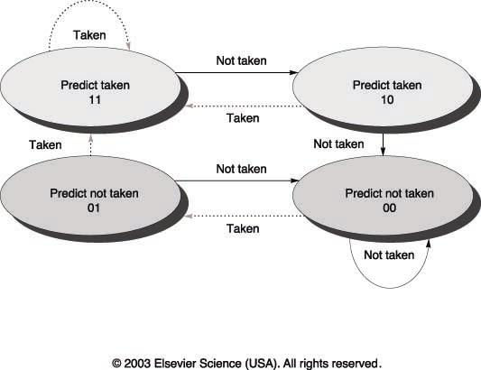
48 2-bit Prediction Scheme This method is more reliable than using a single bit to represent whether the branch was recently taken or not. The use of a 2-bit predictor will allow branches that favor taken (or not taken) to be mispredicted less often than the onebit case.
49
50 Branch Predictors The size of a branch predictor memory will only increase it s effectiveness so much. We also need to address the effectiveness of the scheme used. Just increasing the number of bits in the predictor doesn t do very much either. Some other predictors include: Correlating Predictors Tournament Predictors
51 Branch Predictors Correlating predictors will use the history of a local branch AND some overall information on how branches are executing to make a decision whether to execute or not. Tournament Predictors are even more sophisticated in that they will use multiple predictors local and global and enable them with a selector to improve accuracy.
52 ARM cores, part 2
53 Plan ARM9 AMBA Cortex-M Cortex-R
54 ARM9
55 Source: [2]

56 ARM9 Source: [2]
57 ARM9 - features Over 5 Billion ARM9 processors have been shipped so far The ARM9 family is the most popular ARM processor family ever 250+ silicon licensees 100+ licensees of the ARM926EJ-S processor ARM9 processors continue to be successfully deployed across a wide range of products and applications. The ARM9 family offers proven, low risk and easy to use designs which reduce costs and enable rapid time to market. The ARM9 family consists of three processors - ARM926EJ-S, ARM946E-S and ARM968E-S
58 ARM9 family features Main features Based on ARMv5TE architecture Efficient 5-stage pipeline for faster throughput and system performance Fetch/Decode/Execute/Memory/Writeback Supports both ARM and Thumb instruction sets Efficient ARM-Thumb interworking allows optimal mix of performance and code density
59 ARM9 family features Main features Harvard architecture - Separate Instruction & Data memory interfaces Increased available memory bandwidth Simultaneous access to I & D memory Improved performance 31 x 32-bit registers 32-bit ALU & barrel shifter Enhanced 32-bit MAC block
60 ARM9 DSP enhancements Single cycle 32x16 multiplier implementation Speeds up all multiply instructions Pipelined design allows one 16x16 or 32x16 to start each cycle New 32x16 and 16x16 multiply instructions Allow independent access to 16-bit halves of registers
61 ARM9 DSP enhancements Gives efficient use of 32-bit bandwidth for packed 16-bit operands ARM ISA provides 32x32 multiply instructions Efficient fractional saturating arithmetic QADD, QSUB, QDADD, QDSUB Count leading zeros instruction CLZ for faster normalisation and division

62 ARM9 features comparison Source: [3]
63 AMBA
64 AMBA - Advanced Microcontroller Bus Architecture AMBA onchip communications standard for designing high-performance embedded microcontrollers introduced by ARM in 1996 A few versions: AHB (Advanced High-performance Bus) ASB (Advanced System Bus) APB (Advanced Peripheral Bus) AXI
65 AMBA first specification Buses defined : Advanced System Bus (ASB) Advanced Peripheral Bus (APB)
66 AMBA 2 specification Buses defined : Advanced High-performance Bus (AHB) - widely used on ARM7, ARM9 and ARM Cortex- M based designs Advanced System Bus (ASB) Advanced Peripheral Bus (APB2 or APB)
67 AMBA 3 specification Buses defined: Advanced extensible Interface (AXI3 or AXI v1.0) - widely used on ARM Cortex-A processors including Cortex-A9 Advanced High-performance Bus Lite (AHB- Lite v1.0) Advanced Peripheral Bus (APB3 v1.0) Advanced Trace Bus (ATB v1.0)
68 AMBA 2 specification Buses defined : AXI Coherency Extensions (ACE) - widely used on the latest ARM Cortex-A processors including Cortex-A7 and Cortex-A15 AXI Coherency Extensions Lite (ACE-Lite) Advanced extensible Interface 4 (AXI4) Advanced extensible Interface 4 Lite (AXI4-Lite) Advanced extensible Interface 4 Stream (AXI4- Stream v1.0) Advanced Trace Bus (ATB v1.1) Advanced Peripheral Bus (APB4 v2.0)
69 APB APB designed for low-power system modules, for example register interfaces on system peripherals optimized for minimal power consumption and reduced interface complexity to support peripheral functions It has to support 32bit and 66 MHz signals.
70 ASB ASB designed for high-performance system modules alternative system bus suitable for use where the high-performance features of AHB are not required supports also the efficient connection of: processors, on-chip memories off-chip external memory interfaces with low-power peripheral macrocell functions
71 AHB AHB designed for high-performance, high clock frequency system modules acts as the high-performance system backbone bus supports the efficient connection of: processors, on-chip memories off-chip external memory interfaces with low-power peripheral macrocell functions
72 AHB Features: single edge clock protocol split transactions several bus masters burst transfers pipelined operations single-cycle bus master handover non-tristate implementation large bus-widths (64/128 bit).
73 AHB - Lite AHB Lite is a subset of AHB This subset simplifies the design for a bus with a single master
74 AXI AXI designed for high-performance, high clock frequency system modules with low latency enables high-frequency operation without using complex bridges provides flexibility in the implementation of interconnect architectures is backward-compatible with existing AHB and APB interfaces.
75 AXI Features: separate address/control and data phases support for unaligned data transfers using byte strobes burst based transactions with only start address issued issuing of multiple outstanding addresses with out of order responses easy addition of register stages to provide timing closure.
76 Typical AMBA system
77 Cortex-M
78 Source: [2]
79 Cortex family Currently Cortex family is strongly introduced to the market by ARM corporation Cortex family consists of three subfamilies: Cortex-M cores for microcontrollers and costsensitive applications; Thumb-2 instructions supported
80 Cortex family Cortex family consists of three subfamilies: Cortex-R cores for real time systems appliactions; ARM, Thumb and Thumb-2 instructions supported Cortex-A the most complex and the most powerful cores, for multimedia devices and application processors; ARM, Thumb and Thumb-2 instructions supported

81 Cortex-M Source: [4]

82 Cortex-M
83 Cortex-M Main features: 32-bit processor 3 stage pipelining Thumb-2 instruction list concise and efficient code Many power saving modes and domains Nested Vectored Interrupt Controller well defined times and methods of interrupts invoking RTOS support Debugger support (JTAG, SWD Serial Wire Debug)
84 Cortex-M0/M0+ Source: [2]
85 Cortex-M0/M0+ Source: [2]
86 Cortex-M0 Main features: The armest version of ARM cores The most power saving version of ARM cores only 85mW/MHz Upward compatibility with Cortex-M3 Only gates Only 56 C-optimized instructions Support for low power wireless communication: Bluetooth Low Energy (BLE), ZigBee, etc. Performance 0.9 DMIPS/MHz Single cycle 32x32 multiply instructions Interrupt execution delay: 16 cycles
87 Cortex-M0 Source: [2]
88 Cortex-M0 Processor modes: Thread mode: Used to execute application software. The processor enters Thread mode when it comes out of reset. Handler mode: Used to handle exceptions. The processor returns to Thread mode when it has finished all exception processing.
89 Cortex-M0 core registers
90 Cortex-M0 memory map
91 Cortex-M0 vector table
92 Cortex-M0 register stacking
93 Cortex-M1 Source: [2]
 to ASIC (production) Source:")
94 Cortex-M1 Main features: Core destined for FPGA applications Support for Actel, Altera and Xilinx chips Easy migration from FPGA (development) to ASIC (production) Source: [2]
95 Cortex-M1 Main features: A general-purpose 32-bit microprocessor, which executes the ARMv6-M subset of the Thumb-2 instruction set and offers high performance operation and small size in FPGAs. It has: a three-stage pipeline a three-cycle hardware multiplier little-endian format for accessing all memory. A system control block containing memory-mapped control registers. Source: [2]
96 Cortex-M1 Main features: An integrated Operating System (OS) extensions system timer. An integrated Nested Vectored Interrupt Controller (NVIC) for low-latency interrupt processing. A memory model that supports accesses to both memory and peripheral registers. Integrated and configurable Tightly Coupled Memories (TCMs) Optional debug support. Source: [2]
97 Cortex-M1 Source: [2]
98 Cortex-M1 Processor modes as in Cortex-M0 Source: [2]
99 Cortex-M1 Memory Map Source: [2]
100 Cortex-M3 Source: [2]
101 Cortex-M3 Main features: Introduced to the market in 2004 Destined for the most demanding microcontrollers High performance and many additional features Low power consumption (12.5 DMIPS/mW) Up to 240 interrupt sources!!! Support for many serial protocols
102 Cortex-M3 Main features: Performance of 1.25DMIPS/MHz Support for bit operations Single cycle 32x32bit multiply; 2-12 cycle division Three stage pipelining with branch prediction Memory Protection Unit (MPU) Max speed: up to 275 MHz /340 DMIPS
103 Cortex-M3
104 Cortex-M3 Core features: Thumb instruction set (ARMv7) Banked Stack Pointer Hardware integer divide instructions Automatic processor state saving and restoration for low latency Interrupt Service Routine (ISR) entry and exit.
105 Cortex-M3 NVIC (Nested Vector Interrupt Controller) features: External interrupts, configurable from 1 to 240. Bits of priority, configurable from 3 to 8. Dynamic reprioritization of interrupts. Priority grouping - selection of preempting interrupt levels and non preempting interrupt levels. Support for tail-chaining and late arrival of interrupts. This enables back-to-back interrupt processing without the overhead of state saving and restoration between interrupts. Processor state automatically saved on interrupt entry, and restored on interrupt exit, with no instruction overhead. Optional Wake-up Interrupt Controller (WIC), providing ultra-low power sleep mode support.
106 Cortex-M3 MPU features features: Eight memory regions. Sub Region Disable (SRD), enabling efficient use of memory regions. The ability to enable a background region that implements the default memory map attributes.
107 Cortex-M3 Bus interfaces: Three Advanced High-performance Bus-Lite (AHB-Lite) interfaces: ICode, DCode, and System bus interfaces. Private Peripheral Bus (PPB) based on Advanced Peripheral Bus (APB) interface. Bit-band support that includes atomic bit-band write and read operations. Memory access alignment. Write buffer for buffering of write data. Exclusive access transfers for multiprocessor systems.
108 Cortex-M3 The processor supports two modes of operation, Thread mode and Handler mode: The processor enters Thread mode on Reset, or as a result of an exception return. Privileged and Unprivileged code can run in Thread mode. The processor enters Handler mode as a result of an exception. All code is privileged in Handler mode.
109 Cortex-M3 The processor can operate in one of two operating states: Thumb state. This is normal execution running 16-bit and 32-bit halfword aligned Thumb instructions. Debug State. This is the state when the processor is in halting debug.
110 Cortex-M3
111 Cortex-M3 bit band mapping
112 Cortex-M4 Source: [2]
113 Cortex-M4 Main features: The richest version of Cortex-M subfamily Destined for low power digital signal applications Integrated 32b CPU and DSP Single precision FPU unit Other features like in Cortex-M3 DSP instructions Max speed: up to 300 MHz /375 DMIPS
114 Cortex-M4
115 Cortex-M4 FPU features: 32-bit instructions for single-precision (C float) dataprocessing operations. Combined Multiply and Accumulate instructions for increased precision (Fused MAC). Hardware support for conversion, addition, subtraction, multiplication with optional accumulate, division, and square-root. Hardware support for denormals and all IEEE rounding modes. 32 dedicated 32-bit single precision registers, also addressable as 16 double-word registers. Decoupled three stage pipeline.
116 Cortex-M4 - FPU FPU registers: sixteen 64-bit doubleword registers, D0-D15 or thirty-two 32-bit single-word registers, S0- S31

117 Cortex-R4 Source: [2]
118 Cortex-R4 Main features: A mid-range processor for use in deeply-embedded, real-time systems Includes Thumb-2 technology for optimum code density and processing throughput Integrated 32b CPU and DSP Single precision FPU unit (in versions R4F) ARM and Thumb instructions Tightly-Coupled Memory (TCM) ports for low-latency and deterministic accesses to local RAM, in addition to caches for higher performance to general memory
119 Cortex-R4 Main features: High-speed Advanced Microprocessor Bus Architecture (AMBA) Advanced extensible Interfaces (AXI) for master and slave interfaces Dynamic branch prediction with a global history buffer, and a 4-entry return stack The ability to implement and use redundant core logic, for example, in fault detection ECC Error Corrcting Codes - Optional singlebit error correction and two-bit error detection for cache and/or TCM memories with ECC bits
120 Cortex-R4 Main features: A Harvard L1 memory system with: optional Tightly-Coupled Memory (TCM) interfaces with support for error correction or parity checking memories optional caches with support for optional error correction schemes optional ARMv7-R architecture Memory Protection Unit (MPU) optional parity and Error Checking and Correction (ECC) on all RAM blocks. An L2 memory interface: single 64-bit master AXI interface 64-bit slave AXI interface to TCM RAM blocks and cache RAM blocks.
121 Cortex-R4 Main features: A Harvard L1 memory system with: optional Tightly-Coupled Memory (TCM) interfaces with support for error correction or parity checking memories optional caches with support for optional error correction schemes optional ARMv7-R architecture Memory Protection Unit (MPU) optional parity and Error Checking and Correction (ECC) on all RAM blocks. An L2 memory interface: single 64-bit master AXI interface 64-bit slave AXI interface to TCM RAM blocks and cache RAM blocks.
122 Cortex-R4 Operating modes: User (USR) mode - the usual mode for the execution of ARM or Thumb programs. Fast interrupt (FIQ) mode entered on taking a fast interrupt. Interrupt (IRQ) mode entered on taking a normal interrupt. Supervisor (SVC) mode is a protected mode for the operating system entered on taking a Supervisor Call (SVC), formerly SWI. Abort (ABT) mode entered after a data or instruction abort. System (SYS) mode is a privileged user mode for the operating system.
123 Cortex-R4 register set
124 Cortex-R4 status register

125 Cortex-R5 Source: [2]
126 Cortex-R5 Main features: Improved (extended) version of Cortex-R4 processor Added hardware Accelerator Coherency Port (ACP) to reduce the requirement for slow software cache maintenance operations when sharing memory with other master Added Vector Floatin-Point v3 Added Multiprocessing Extensions for multiprocessing functionality Added Low Latency Peripheral Port for integration of latency sensitive peripherals with processor
127 Cortex-R5 Implementation example:
128 Thank you for your attention
129 Cortex-R5 VFP v3-d16: The FPU fully supports single-precision and double-precision add, subtract, multiply, divide,multiply and accumulate, and square root operations provides conversions between fixed-point and floating-point data formats, and floating-point constant instructions includes 16 double-precision registers
130 Cortex-R5 Vector instructions:

131 Cortex-R7 Source: [2]
132 Cortex-R7 Main features: The highest perfoming Cortex-R processor On a 40 nm G process the Cortex-R7 processor can be implemented to run at well over 1 GHz when it delivers over 2700 Dhrystone MIPS performance On a 28nm process the perfomance is estimated to reach 4600 Dhrystone MIPS
133 Cortex-R7 Main features: Eleven-stage pipeline with instruction prefetch, branch prediction, superscalar and out of order execution divide and floating-point 2.53 Dhrystone MIPS/MHz Added LLRAM low latency memory port designed specifically to connect to local memory (64-bit)
134 Thank you for your attention
135 References [1] ARM7TDMI core documentation; [2] [3] ARM9 family documentation; [4] Cortex family documentation; [5] ipelining: Basic and Intermediate Concepts
ADVANCED PROCESSOR ARCHITECTURES AND MEMORY ORGANISATION Lesson-12: ARM
 ADVANCED PROCESSOR ARCHITECTURES AND MEMORY ORGANISATION Lesson-12: ARM 1 The ARM architecture processors popular in Mobile phone systems 2 ARM Features ARM has 32-bit architecture but supports 16 bit
ARM Microprocessor and ARM-Based Microcontrollers
 ARM Microprocessor and ARM-Based Microcontrollers Nguatem William 24th May 2006 A Microcontroller-Based Embedded System Roadmap 1 Introduction ARM ARM Basics 2 ARM Extensions Thumb Jazelle NEON & DSP Enhancement
An Introduction to the ARM 7 Architecture
 An Introduction to the ARM 7 Architecture Trevor Martin CEng, MIEE Technical Director This article gives an overview of the ARM 7 architecture and a description of its major features for a developer new
Overview of the Cortex-M3
 CHAPTER Overview of the Cortex-M3 2 In This Chapter Fundamentals 11 Registers 12 Operation Modes 14 The Built-In Nested Vectored Interrupt Controller 15 The Memory Map 16 The Bus Interface 17 The MPU 18
Pipeline Hazards. Structure hazard Data hazard. ComputerArchitecture_PipelineHazard1
 Pipeline Hazards Structure hazard Data hazard Pipeline hazard: the major hurdle A hazard is a condition that prevents an instruction in the pipe from executing its next scheduled pipe stage Taxonomy of
 More on Pipelining and Pipelines in Real Machines CS 333 Fall 2006 Main Ideas Data Hazards RAW WAR WAW More pipeline stall reduction techniques Branch prediction» static» dynamic bimodal branch prediction
BEAGLEBONE BLACK ARCHITECTURE MADELEINE DAIGNEAU MICHELLE ADVENA
 BEAGLEBONE BLACK ARCHITECTURE MADELEINE DAIGNEAU MICHELLE ADVENA AGENDA INTRO TO BEAGLEBONE BLACK HARDWARE & SPECS CORTEX-A8 ARMV7 PROCESSOR PROS & CONS VS RASPBERRY PI WHEN TO USE BEAGLEBONE BLACK Single
Exception and Interrupt Handling in ARM
 Exception and Interrupt Handling in ARM Architectures and Design Methods for Embedded Systems Summer Semester 2006 Author: Ahmed Fathy Mohammed Abdelrazek Advisor: Dominik Lücke Abstract We discuss exceptions
Solution: start more than one instruction in the same clock cycle CPI < 1 (or IPC > 1, Instructions per Cycle) Two approaches:
 Two approaches:") Multiple-Issue Processors Pipelining can achieve CPI close to 1 Mechanisms for handling hazards Static or dynamic scheduling Static or dynamic branch handling Increase in transistor counts (Moore s Law):
Multiple-Issue Processors Pipelining can achieve CPI close to 1 Mechanisms for handling hazards Static or dynamic scheduling Static or dynamic branch handling Increase in transistor counts (Moore s Law):
Digitale Signalverarbeitung mit FPGA (DSF) Soft Core Prozessor NIOS II Stand Mai 2007. Jens Onno Krah
 Soft Core Prozessor NIOS II Stand Mai 2007. Jens Onno Krah") (DSF) Soft Core Prozessor NIOS II Stand Mai 2007 Jens Onno Krah Cologne University of Applied Sciences www.fh-koeln.de jens_onno.krah@fh-koeln.de NIOS II 1 1 What is Nios II? Altera s Second Generation
(DSF) Soft Core Prozessor NIOS II Stand Mai 2007 Jens Onno Krah Cologne University of Applied Sciences www.fh-koeln.de jens_onno.krah@fh-koeln.de NIOS II 1 1 What is Nios II? Altera s Second Generation
Five Families of ARM Processor IP
 ARM1026EJ-S Synthesizable ARM10E Family Processor Core Eric Schorn CPU Product Manager ARM Austin Design Center Five Families of ARM Processor IP Performance ARM preserves SW & HW investment through code
The ARM Architecture. With a focus on v7a and Cortex-A8
 The ARM Architecture With a focus on v7a and Cortex-A8 1 Agenda Introduction to ARM Ltd ARM Processors Overview ARM v7a Architecture/Programmers Model Cortex-A8 Memory Management Cortex-A8 Pipeline 2 ARM
Q. Consider a dynamic instruction execution (an execution trace, in other words) that consists of repeats of code in this pattern:
 that consists of repeats of code in this pattern:") Pipelining HW Q. Can a MIPS SW instruction executing in a simple 5-stage pipelined implementation have a data dependency hazard of any type resulting in a nop bubble? If so, show an example; if not, prove
Pipelining HW Q. Can a MIPS SW instruction executing in a simple 5-stage pipelined implementation have a data dependency hazard of any type resulting in a nop bubble? If so, show an example; if not, prove
Exploring the Design of the Cortex-A15 Processor ARM s next generation mobile applications processor. Travis Lanier Senior Product Manager
 Exploring the Design of the Cortex-A15 Processor ARM s next generation mobile applications processor Travis Lanier Senior Product Manager 1 Cortex-A15: Next Generation Leadership Cortex-A class multi-processor
Migrating Application Code from ARM Cortex-M4 to Cortex-M7 Processors
 Migrating Application Code from ARM Cortex-M4 to Cortex-M7 Processors Joseph Yiu and Robert Boys January 2015 Version 1.1 The latest version of this document is here: /appnotes/docs/apnt_270.asp 1 Cortex
150127-Microprocessor & Assembly Language
 Chapter 3 Z80 Microprocessor Architecture The Z 80 is one of the most talented 8 bit microprocessors, and many microprocessor-based systems are designed around the Z80. The Z80 microprocessor needs an
ARM Ltd 110 Fulbourn Road, Cambridge, CB1 9NJ, UK. *peter.harrod@arm.com
 Serial Wire Debug and the CoreSight TM Debug and Trace Architecture Eddie Ashfield, Ian Field, Peter Harrod *, Sean Houlihane, William Orme and Sheldon Woodhouse ARM Ltd 110 Fulbourn Road, Cambridge, CB1
Which ARM Cortex Core Is Right for Your Application: A, R or M?
 Which ARM Cortex Core Is Right for Your Application: A, R or M? Introduction The ARM Cortex series of cores encompasses a very wide range of scalable performance options offering designers a great deal
INSTRUCTION LEVEL PARALLELISM PART VII: REORDER BUFFER
 Course on: Advanced Computer Architectures INSTRUCTION LEVEL PARALLELISM PART VII: REORDER BUFFER Prof. Cristina Silvano Politecnico di Milano cristina.silvano@polimi.it Prof. Silvano, Politecnico di Milano
A Survey on ARM Cortex A Processors. Wei Wang Tanima Dey
 A Survey on ARM Cortex A Processors Wei Wang Tanima Dey 1 Overview of ARM Processors Focusing on Cortex A9 & Cortex A15 ARM ships no processors but only IP cores For SoC integration Targeting markets:
Chapter 13. PIC Family Microcontroller
 Chapter 13 PIC Family Microcontroller Lesson 01 PIC Characteristics and Examples PIC microcontroller characteristics Power-on reset Brown out reset Simplified instruction set High speed execution Up to
ARM Processors and the Internet of Things. Joseph Yiu Senior Embedded Technology Specialist, ARM
 ARM Processors and the Internet of Things Joseph Yiu Senior Embedded Technology Specialist, ARM 1 Internet of Things is a very Diverse Market Human interface Location aware MEMS sensors Smart homes Security,
CS352H: Computer Systems Architecture
 CS352H: Computer Systems Architecture Topic 9: MIPS Pipeline - Hazards October 1, 2009 University of Texas at Austin CS352H - Computer Systems Architecture Fall 2009 Don Fussell Data Hazards in ALU Instructions
Cortex-A9 MPCore Software Development
 Cortex-A9 MPCore Software Development Course Description Cortex-A9 MPCore software development is a 4 days ARM official course. The course goes into great depth and provides all necessary know-how to develop
Introduction to Cloud Computing
 Introduction to Cloud Computing Parallel Processing I 15 319, spring 2010 7 th Lecture, Feb 2 nd Majd F. Sakr Lecture Motivation Concurrency and why? Different flavors of parallel computing Get the basic
IA-64 Application Developer s Architecture Guide
 IA-64 Application Developer s Architecture Guide The IA-64 architecture was designed to overcome the performance limitations of today s architectures and provide maximum headroom for the future. To achieve
(Refer Slide Time: 00:01:16 min)
") Digital Computer Organization Prof. P. K. Biswas Department of Electronic & Electrical Communication Engineering Indian Institute of Technology, Kharagpur Lecture No. # 04 CPU Design: Tirning & Control
Digital Computer Organization Prof. P. K. Biswas Department of Electronic & Electrical Communication Engineering Indian Institute of Technology, Kharagpur Lecture No. # 04 CPU Design: Tirning & Control
Architectures, Processors, and Devices
 Architectures, Processors, and Devices Development Article Copyright 2009 ARM Limited. All rights reserved. ARM DHT 0001A Development Article Copyright 2009 ARM Limited. All rights reserved. Release Information
The ARM Cortex-A9 Processors
 The ARM Cortex-A9 Processors This whitepaper describes the details of a newly developed processor design within the common ARM Cortex applications profile ARM Cortex-A9 MPCore processor: A multicore processor
7a. System-on-chip design and prototyping platforms
 7a. System-on-chip design and prototyping platforms Labros Bisdounis, Ph.D. Department of Computer and Communication Engineering 1 What is System-on-Chip (SoC)? System-on-chip is an integrated circuit
Software based Finite State Machine (FSM) with general purpose processors
 with general purpose processors") Software based Finite State Machine (FSM) with general purpose processors White paper Joseph Yiu January 2013 Overview Finite state machines (FSM) are commonly used in electronic designs. FSM can be used
Software based Finite State Machine (FSM) with general purpose processors White paper Joseph Yiu January 2013 Overview Finite state machines (FSM) are commonly used in electronic designs. FSM can be used
Introduction to RISC Processor. ni logic Pvt. Ltd., Pune
 Introduction to RISC Processor ni logic Pvt. Ltd., Pune AGENDA What is RISC & its History What is meant by RISC Architecture of MIPS-R4000 Processor Difference Between RISC and CISC Pros and Cons of RISC
Advanced Computer Architecture-CS501. Computer Systems Design and Architecture 2.1, 2.2, 3.2
 Lecture Handout Computer Architecture Lecture No. 2 Reading Material Vincent P. Heuring&Harry F. Jordan Chapter 2,Chapter3 Computer Systems Design and Architecture 2.1, 2.2, 3.2 Summary 1) A taxonomy of
ADVANCED PROCESSOR ARCHITECTURES AND MEMORY ORGANISATION Lesson-17: Memory organisation, and types of memory
 ADVANCED PROCESSOR ARCHITECTURES AND MEMORY ORGANISATION Lesson-17: Memory organisation, and types of memory 1 1. Memory Organisation 2 Random access model A memory-, a data byte, or a word, or a double
Application Note 195. ARM11 performance monitor unit. Document number: ARM DAI 195B Issued: 15th February, 2008 Copyright ARM Limited 2007
 Application Note 195 ARM11 performance monitor unit Document number: ARM DAI 195B Issued: 15th February, 2008 Copyright ARM Limited 2007 Copyright 2007 ARM Limited. All rights reserved. Application Note
CHAPTER 7: The CPU and Memory
 CHAPTER 7: The CPU and Memory The Architecture of Computer Hardware, Systems Software & Networking: An Information Technology Approach 4th Edition, Irv Englander John Wiley and Sons 2010 PowerPoint slides
Week 1 out-of-class notes, discussions and sample problems
 Week 1 out-of-class notes, discussions and sample problems Although we will primarily concentrate on RISC processors as found in some desktop/laptop computers, here we take a look at the varying types
Chapter 1 Computer System Overview
 Operating Systems: Internals and Design Principles Chapter 1 Computer System Overview Eighth Edition By William Stallings Operating System Exploits the hardware resources of one or more processors Provides
MACHINE ARCHITECTURE & LANGUAGE
 in the name of God the compassionate, the merciful notes on MACHINE ARCHITECTURE & LANGUAGE compiled by Jumong Chap. 9 Microprocessor Fundamentals A system designer should consider a microprocessor-based
EE482: Advanced Computer Organization Lecture #11 Processor Architecture Stanford University Wednesday, 31 May 2000. ILP Execution
 EE482: Advanced Computer Organization Lecture #11 Processor Architecture Stanford University Wednesday, 31 May 2000 Lecture #11: Wednesday, 3 May 2000 Lecturer: Ben Serebrin Scribe: Dean Liu ILP Execution
CHAPTER 4 MARIE: An Introduction to a Simple Computer
 CHAPTER 4 MARIE: An Introduction to a Simple Computer 4.1 Introduction 195 4.2 CPU Basics and Organization 195 4.2.1 The Registers 196 4.2.2 The ALU 197 4.2.3 The Control Unit 197 4.3 The Bus 197 4.4 Clocks
WAR: Write After Read
 WAR: Write After Read write-after-read (WAR) = artificial (name) dependence add R1, R2, R3 sub R2, R4, R1 or R1, R6, R3 problem: add could use wrong value for R2 can t happen in vanilla pipeline (reads
Central Processing Unit (CPU)
") Central Processing Unit (CPU) CPU is the heart and brain It interprets and executes machine level instructions Controls data transfer from/to Main Memory (MM) and CPU Detects any errors In the following
Central Processing Unit (CPU) CPU is the heart and brain It interprets and executes machine level instructions Controls data transfer from/to Main Memory (MM) and CPU Detects any errors In the following
Pipelining Review and Its Limitations
 Pipelining Review and Its Limitations Yuri Baida yuri.baida@gmail.com yuriy.v.baida@intel.com October 16, 2010 Moscow Institute of Physics and Technology Agenda Review Instruction set architecture Basic
ARM Webinar series. ARM Based SoC. Abey Thomas
 ARM Webinar series ARM Based SoC Verification Abey Thomas Agenda About ARM and ARM IP ARM based SoC Verification challenges Verification planning and strategy IP Connectivity verification Performance verification
All Programmable Logic. Hans-Joachim Gelke Institute of Embedded Systems. Zürcher Fachhochschule
 All Programmable Logic Hans-Joachim Gelke Institute of Embedded Systems Institute of Embedded Systems 31 Assistants 10 Professors 7 Technical Employees 2 Secretaries www.ines.zhaw.ch Research: Education:
CS:APP Chapter 4 Computer Architecture. Wrap-Up. William J. Taffe Plymouth State University. using the slides of
 CS:APP Chapter 4 Computer Architecture Wrap-Up William J. Taffe Plymouth State University using the slides of Randal E. Bryant Carnegie Mellon University Overview Wrap-Up of PIPE Design Performance analysis
Lecture: Pipelining Extensions. Topics: control hazards, multi-cycle instructions, pipelining equations
 Lecture: Pipelining Extensions Topics: control hazards, multi-cycle instructions, pipelining equations 1 Problem 6 Show the instruction occupying each stage in each cycle (with bypassing) if I1 is R1+R2
A Lab Course on Computer Architecture
 A Lab Course on Computer Architecture Pedro López José Duato Depto. de Informática de Sistemas y Computadores Facultad de Informática Universidad Politécnica de Valencia Camino de Vera s/n, 46071 - Valencia,
Central Processing Unit
 Chapter 4 Central Processing Unit 1. CPU organization and operation flowchart 1.1. General concepts The primary function of the Central Processing Unit is to execute sequences of instructions representing
Overview. CISC Developments. RISC Designs. CISC Designs. VAX: Addressing Modes. Digital VAX
 Overview CISC Developments Over Twenty Years Classic CISC design: Digital VAX VAXÕs RISC successor: PRISM/Alpha IntelÕs ubiquitous 80x86 architecture Ð 8086 through the Pentium Pro (P6) RJS 2/3/97 Philosophy
Execution Cycle. Pipelining. IF and ID Stages. Simple MIPS Instruction Formats
 Execution Cycle Pipelining CSE 410, Spring 2005 Computer Systems http://www.cs.washington.edu/410 1. Instruction Fetch 2. Instruction Decode 3. Execute 4. Memory 5. Write Back IF and ID Stages 1. Instruction
İSTANBUL AYDIN UNIVERSITY
 İSTANBUL AYDIN UNIVERSITY FACULTY OF ENGİNEERİNG SOFTWARE ENGINEERING THE PROJECT OF THE INSTRUCTION SET COMPUTER ORGANIZATION GÖZDE ARAS B1205.090015 Instructor: Prof. Dr. HASAN HÜSEYİN BALIK DECEMBER
OpenSPARC T1 Processor
 OpenSPARC T1 Processor The OpenSPARC T1 processor is the first chip multiprocessor that fully implements the Sun Throughput Computing Initiative. Each of the eight SPARC processor cores has full hardware
Switch Fabric Implementation Using Shared Memory
 Order this document by /D Switch Fabric Implementation Using Shared Memory Prepared by: Lakshmi Mandyam and B. Kinney INTRODUCTION Whether it be for the World Wide Web or for an intra office network, today
Architectures and Platforms
 Hardware/Software Codesign Arch&Platf. - 1 Architectures and Platforms 1. Architecture Selection: The Basic Trade-Offs 2. General Purpose vs. Application-Specific Processors 3. Processor Specialisation
VLIW Processors. VLIW Processors
 1 VLIW Processors VLIW ( very long instruction word ) processors instructions are scheduled by the compiler a fixed number of operations are formatted as one big instruction (called a bundle) usually LIW
Applying the Benefits of Network on a Chip Architecture to FPGA System Design
 Applying the Benefits of on a Chip Architecture to FPGA System Design WP-01149-1.1 White Paper This document describes the advantages of network on a chip (NoC) architecture in Altera FPGA system design.
what operations can it perform? how does it perform them? on what kind of data? where are instructions and data stored?
 Inside the CPU how does the CPU work? what operations can it perform? how does it perform them? on what kind of data? where are instructions and data stored? some short, boring programs to illustrate the
Let s put together a Manual Processor
 Lecture 14 Let s put together a Manual Processor Hardware Lecture 14 Slide 1 The processor Inside every computer there is at least one processor which can take an instruction, some operands and produce
An Overview of Stack Architecture and the PSC 1000 Microprocessor
 An Overview of Stack Architecture and the PSC 1000 Microprocessor Introduction A stack is an important data handling structure used in computing. Specifically, a stack is a dynamic set of elements in which
How To Design A Single Chip System Bus (Amba) For A Single Threaded Microprocessor (Mma) (I386) (Mmb) (Microprocessor) (Ai) (Bower) (Dmi) (Dual
 For A Single Threaded Microprocessor (Mma) (I386) (Mmb) (Microprocessor) (Ai) (Bower) (Dmi) (Dual") Architetture di bus per System-On On-Chip Massimo Bocchi Corso di Architettura dei Sistemi Integrati A.A. 2002/2003 System-on on-chip motivations 400 300 200 100 0 19971999 2001 2003 2005 2007 2009 Transistors
Architetture di bus per System-On On-Chip Massimo Bocchi Corso di Architettura dei Sistemi Integrati A.A. 2002/2003 System-on on-chip motivations 400 300 200 100 0 19971999 2001 2003 2005 2007 2009 Transistors
Computer Organization and Components
 Computer Organization and Components IS5, fall 25 Lecture : Pipelined Processors ssociate Professor, KTH Royal Institute of Technology ssistant Research ngineer, University of California, Berkeley Slides
Computer Architecture Lecture 2: Instruction Set Principles (Appendix A) Chih Wei Liu 劉 志 尉 National Chiao Tung University cwliu@twins.ee.nctu.edu.
 Chih Wei Liu 劉 志 尉 National Chiao Tung University cwliu@twins.ee.nctu.edu.") Computer Architecture Lecture 2: Instruction Set Principles (Appendix A) Chih Wei Liu 劉 志 尉 National Chiao Tung University cwliu@twins.ee.nctu.edu.tw Review Computers in mid 50 s Hardware was expensive
Computer Architecture Lecture 2: Instruction Set Principles (Appendix A) Chih Wei Liu 劉 志 尉 National Chiao Tung University cwliu@twins.ee.nctu.edu.tw Review Computers in mid 50 s Hardware was expensive
Chapter 2 Basic Structure of Computers. Jin-Fu Li Department of Electrical Engineering National Central University Jungli, Taiwan
 Chapter 2 Basic Structure of Computers Jin-Fu Li Department of Electrical Engineering National Central University Jungli, Taiwan Outline Functional Units Basic Operational Concepts Bus Structures Software
Am186ER/Am188ER AMD Continues 16-bit Innovation
 Am186ER/Am188ER AMD Continues 16-bit Innovation 386-Class Performance, Enhanced System Integration, and Built-in SRAM Problem with External RAM All embedded systems require RAM Low density SRAM moving
STM32 F-2 series High-performance Cortex-M3 MCUs
 STM32 F-2 series High-performance Cortex-M3 MCUs STMicroelectronics 32-bit microcontrollers, 120 MHz/150 DMIPS with ART Accelerator TM and advanced peripherals www.st.com/mcu STM32 F-2 series The STM32
Instruction Set Design
 Instruction Set Design Instruction Set Architecture: to what purpose? ISA provides the level of abstraction between the software and the hardware One of the most important abstraction in CS It s narrow,
StrongARM** SA-110 Microprocessor Instruction Timing
 StrongARM** SA-110 Microprocessor Instruction Timing Application Note September 1998 Order Number: 278194-001 Information in this document is provided in connection with Intel products. No license, express
AMD Opteron Quad-Core
 AMD Opteron Quad-Core a brief overview Daniele Magliozzi Politecnico di Milano Opteron Memory Architecture native quad-core design (four cores on a single die for more efficient data sharing) enhanced
COMPUTER HARDWARE. Input- Output and Communication Memory Systems
 COMPUTER HARDWARE Input- Output and Communication Memory Systems Computer I/O I/O devices commonly found in Computer systems Keyboards Displays Printers Magnetic Drives Compact disk read only memory (CD-ROM)
LogiCORE IP AXI Performance Monitor v2.00.a
 LogiCORE IP AXI Performance Monitor v2.00.a Product Guide Table of Contents IP Facts Chapter 1: Overview Target Technology................................................................. 9 Applications......................................................................
LSN 2 Computer Processors
 LSN 2 Computer Processors Department of Engineering Technology LSN 2 Computer Processors Microprocessors Design Instruction set Processor organization Processor performance Bandwidth Clock speed LSN 2
Hardware accelerated Virtualization in the ARM Cortex Processors
 Hardware accelerated Virtualization in the ARM Cortex Processors John Goodacre Director, Program Management ARM Processor Division ARM Ltd. Cambridge UK 2nd November 2010 Sponsored by: & & New Capabilities
Cortex -A15. Technical Reference Manual. Revision: r2p0. Copyright 2011 ARM. All rights reserved. ARM DDI 0438C (ID102211)
") Cortex -A15 Revision: r2p0 Technical Reference Manual Copyright 2011 ARM. All rights reserved. ARM DDI 0438C () Cortex-A15 Technical Reference Manual Copyright 2011 ARM. All rights reserved. Release Information
Cortex -A15 Revision: r2p0 Technical Reference Manual Copyright 2011 ARM. All rights reserved. ARM DDI 0438C () Cortex-A15 Technical Reference Manual Copyright 2011 ARM. All rights reserved. Release Information
Lecture 11: Multi-Core and GPU. Multithreading. Integration of multiple processor cores on a single chip.
 Lecture 11: Multi-Core and GPU Multi-core computers Multithreading GPUs General Purpose GPUs Zebo Peng, IDA, LiTH 1 Multi-Core System Integration of multiple processor cores on a single chip. To provide
PROBLEMS #20,R0,R1 #$3A,R2,R4
 506 CHAPTER 8 PIPELINING (Corrisponde al cap. 11 - Introduzione al pipelining) PROBLEMS 8.1 Consider the following sequence of instructions Mul And #20,R0,R1 #3,R2,R3 #$3A,R2,R4 R0,R2,R5 In all instructions,
Computer Performance. Topic 3. Contents. Prerequisite knowledge Before studying this topic you should be able to:
 55 Topic 3 Computer Performance Contents 3.1 Introduction...................................... 56 3.2 Measuring performance............................... 56 3.2.1 Clock Speed.................................
UNIVERSITY OF CALIFORNIA, DAVIS Department of Electrical and Computer Engineering. EEC180B Lab 7: MISP Processor Design Spring 1995
 UNIVERSITY OF CALIFORNIA, DAVIS Department of Electrical and Computer Engineering EEC180B Lab 7: MISP Processor Design Spring 1995 Objective: In this lab, you will complete the design of the MISP processor,
CISC, RISC, and DSP Microprocessors
 CISC, RISC, and DSP Microprocessors Douglas L. Jones ECE 497 Spring 2000 4/6/00 CISC, RISC, and DSP D.L. Jones 1 Outline Microprocessors circa 1984 RISC vs. CISC Microprocessors circa 1999 Perspective:
SoC IP Interfaces and Infrastructure A Hybrid Approach
 SoC IP Interfaces and Infrastructure A Hybrid Approach Cary Robins, Shannon Hill ChipWrights, Inc. ABSTRACT System-On-Chip (SoC) designs incorporate more and more Intellectual Property (IP) with each year.
Instruction Set Architecture. or How to talk to computers if you aren t in Star Trek
 Instruction Set Architecture or How to talk to computers if you aren t in Star Trek The Instruction Set Architecture Application Compiler Instr. Set Proc. Operating System I/O system Instruction Set Architecture
Chapter 2 Logic Gates and Introduction to Computer Architecture
 Chapter 2 Logic Gates and Introduction to Computer Architecture 2.1 Introduction The basic components of an Integrated Circuit (IC) is logic gates which made of transistors, in digital system there are
An Implementation Of Multiprocessor Linux
 An Implementation Of Multiprocessor Linux This document describes the implementation of a simple SMP Linux kernel extension and how to use this to develop SMP Linux kernels for architectures other than
Digital Signal Controller Based Automatic Transfer Switch
 Digital Signal Controller Based Automatic Transfer Switch by Venkat Anant Senior Staff Applications Engineer Freescale Semiconductor, Inc. Abstract: An automatic transfer switch (ATS) enables backup generators,
Learning Outcomes. Simple CPU Operation and Buses. Composition of a CPU. A simple CPU design
 Learning Outcomes Simple CPU Operation and Buses Dr Eddie Edwards eddie.edwards@imperial.ac.uk At the end of this lecture you will Understand how a CPU might be put together Be able to name the basic components
Design of Pipelined MIPS Processor. Sept. 24 & 26, 1997
 Design of Pipelined MIPS Processor Sept. 24 & 26, 1997 Topics Instruction processing Principles of pipelining Inserting pipe registers Data Hazards Control Hazards Exceptions MIPS architecture subset R-type
Chapter 5 Instructor's Manual
 The Essentials of Computer Organization and Architecture Linda Null and Julia Lobur Jones and Bartlett Publishers, 2003 Chapter 5 Instructor's Manual Chapter Objectives Chapter 5, A Closer Look at Instruction
Embedded Systems on ARM Cortex-M3 (4weeks/45hrs)
") Embedded Systems on ARM Cortex-M3 (4weeks/45hrs) Course & Kit Contents LEARN HOW TO: Use of Keil Real View for ARM Use ARM Cortex-M3 MCU for professional embedded application development Understanding
Embedded Systems on ARM Cortex-M3 (4weeks/45hrs) Course & Kit Contents LEARN HOW TO: Use of Keil Real View for ARM Use ARM Cortex-M3 MCU for professional embedded application development Understanding
MICROPROCESSOR AND MICROCOMPUTER BASICS
 Introduction MICROPROCESSOR AND MICROCOMPUTER BASICS At present there are many types and sizes of computers available. These computers are designed and constructed based on digital and Integrated Circuit
PART B QUESTIONS AND ANSWERS UNIT I
 PART B QUESTIONS AND ANSWERS UNIT I 1. Explain the architecture of 8085 microprocessor? Logic pin out of 8085 microprocessor Address bus: unidirectional bus, used as high order bus Data bus: bi-directional
Addressing The problem. When & Where do we encounter Data? The concept of addressing data' in computations. The implications for our machine design(s)
") Addressing The problem Objectives:- When & Where do we encounter Data? The concept of addressing data' in computations The implications for our machine design(s) Introducing the stack-machine concept Slide
Addressing The problem Objectives:- When & Where do we encounter Data? The concept of addressing data' in computations The implications for our machine design(s) Introducing the stack-machine concept Slide
EE361: Digital Computer Organization Course Syllabus
 EE361: Digital Computer Organization Course Syllabus Dr. Mohammad H. Awedh Spring 2014 Course Objectives Simply, a computer is a set of components (Processor, Memory and Storage, Input/Output Devices)
Embedded Development Tools
 Embedded Development Tools Software Development Tools by ARM ARM tools enable developers to get the best from their ARM technology-based systems. Whether implementing an ARM processor-based SoC, writing
Von der Hardware zur Software in FPGAs mit Embedded Prozessoren. Alexander Hahn Senior Field Application Engineer Lattice Semiconductor
 Von der Hardware zur Software in FPGAs mit Embedded Prozessoren Alexander Hahn Senior Field Application Engineer Lattice Semiconductor AGENDA Overview Mico32 Embedded Processor Development Tool Chain HW/SW
MICROPROCESSOR. Exclusive for IACE Students www.iace.co.in iacehyd.blogspot.in Ph: 9700077455/422 Page 1
 MICROPROCESSOR A microprocessor incorporates the functions of a computer s central processing unit (CPU) on a single Integrated (IC), or at most a few integrated circuit. It is a multipurpose, programmable
Giving credit where credit is due
 CSCE 230J Computer Organization Processor Architecture VI: Wrap-Up Dr. Steve Goddard goddard@cse.unl.edu http://cse.unl.edu/~goddard/courses/csce230j Giving credit where credit is due ost of slides for
Computer organization
 Computer organization Computer design an application of digital logic design procedures Computer = processing unit + memory system Processing unit = control + datapath Control = finite state machine inputs
Debug and Trace for Multicore SoCs How to build an efficient and effective debug and trace system for complex, multicore SoCs
 Debug and Trace for Multicore SoCs How to build an efficient and effective debug and trace system for complex, multicore SoCs William Orme September 2008 Abstract As SoC designs become ever more complex