ECE 331: Introduction to Materials for Electrical Engineers
|
|
|
- Abel Wood
- 9 years ago
- Views:
Transcription
1 ECE 331: Introduction to Materials for Electrical Engineers Course Objective... Introduce fundamental concepts in Materials Science and how they are used in ECE You will learn about: material structure how structure dictates properties how electronic & physical properties are related This course will help you to: use materials properly realize new design opportunities with materials understand the physics of semiconductor devices

2 ECE 331 Intro to Materials for ECE Materials in ECE are: semiconductors, metals (e.g. Al contacts), t polymers (e.g. encapsulants for LEDs) and insulators (ceramics such as silicon dioxide in FETs) Materials in ECE are single crystals, polycrystals, amorphous layers and nanostructures t Si (silicon) is NOT the only semiconductor (though Si electronics is the world s largest manufacturing industry), but it is the most important one and will remain so!
, but it is the most important one and will remain")
3 ECE 331 Intro to Materials for ECE III-V examples GaAs InP InAs AlGaAs InGaAs InGaAsP GaN InGaN Know your periodic table! Find your old chemistry notes! III -V

4 Materials Roadmap for Device Technologies: the Bandgap vs Lattice Constant Relationship III-V electronics CD Lasers Fiber pump lasers Space solar ECE applications are expanding across this entire space! CMOS, BiCMOS, Terrestrial solar, Power CMOS Telecomm Optoelectronics thermophotovoltaics

5 TECHNOLOGY ROADMAPS: New Age for ECE Materials and opportunities Roadmaps are calling for unusual properties not obtainable using conventional materials or processes Electronics: - Nanoscale patterning - optical interconnects - speed enhancing materials Optoelectronics: - tunable light emission/detection wavelengths - seamless integration with electronic systems Alternative Energy: - clean, renewable, cheap, safe, autonomous - Biocompatiblity and medicine

6 The Materials Selection Process 1. Pick Application Determine required Properties Properties: mechanical, electrical, thermal, magnetic, optical, deteriorative. 2. Properties Identify candidate Material(s) Material: structure, composition. 3. Material Identify required Processing Processing: changes structure and overall shape ex: casting, sintering, vapor deposition, doping forming, joining, annealing.

7 ELECTRICAL Electrical Resistivity of Copper: y, r m) esistivit 0-8 Ohm- Re (10 6 Adapted from Fig. 18.8, Callister 7e. (Fig adapted from: J.O. Linde, 5 Ann Physik 5, 219 (1932); and C.A. Wert and R.M. Thomson, Physics of Solids, 2nd edition, 4 McGraw-Hill Company, New York, 1970.) T ( C) Adding impurity atoms to Cu increases resistivity. Deforming Cu increases resistivity.
 3 2 1 0-200 -100 0 T ( C) Adding impurity atoms to Cu increases resistivity.")
8 THERMAL Space Shuttle Tiles: --Silica fiber insulation offers low heat conduction. Thermal Conductivity of Copper: - decreases when you add zinc! 100mm Adapted from chapteropening photograph, Chapter 19, Callister 7e. (Courtesy of Lockheed Missiles and Space Company, Inc.) Adapted from Fig. 19.4W, Callister 6e. (Courtesy of Lockheed Aerospace Ceramics Systems, Sunnyvale, CA) (Note: "W" denotes fig. is on CD-ROM.) Th hermal Co onductivi ity (W/ /m-k) Composition (wt% Zinc) Adapted from Fig. 19.4, Callister 7e. (Fig is adapted from Metals Handbook: Properties and Selection: Nonferrous alloys and Pure Metals, Vol. 2, 9th ed., H. Baker, (Managing Editor), American Society for Metals, 1979, p. 315.)
 Th hermal Co onductivi ity (W/ /m-k) 400 300 200 100 0 0 10 20 30 40 Composition (wt% Zinc) Adapted from Fig. 19.")
9 MAGNETIC Magnetic Storage: --Recording medium is magnetized by recording head. Magnetic Permeability vs. Composition: --Adding 3 atomic % Si makes Fe a better recording medium! Fig , Callister 7e. (Fig is from J.U. Lemke, MRS Bulletin, Vol. XV, No. 3, p. 31, 1990.) Magnetiz zation Fe+3%Si Fe Magnetic Field Adapted from C.R. Barrett, W.D. Nix, and A.S. Tetelman, The Principles of Engineering Materials, Fig. 1-7(a), p. 9, Electronically reproduced by permission of Pearson Education, Inc., Upper Saddle River, New Jersey.
, p. 9, 1973.")
10 OPTICAL Transmittance: --Aluminum oxide may be transparent, translucent, or opaque depending on the material structure. polycrystal: polycrystal: single crystal low porosity high porosity Adapted from Fig. 1.2, Callister 7e. (Specimen preparation, P.A. Lessing; photo by S. Tanner.)

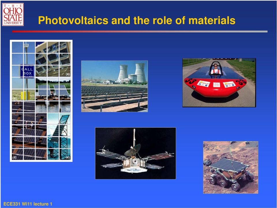
11 Photovoltaics and the role of materials
12
13 Conversion of radiant heat to electricity: Thermophotovoltaics Front Contact Grid Finger Interconnect n InPAs window n/p InGaAs Emitter/Bas e p InPAs BSF p/n InGaAs TJ n InPAs Buffer Semi-Insulating InP SiN/Gold Back Surface Reflector SEM Micrograph Of Processed Ternary MIM Structure Efficiency ~18% With addition of a a front surface filter 0.9 W/cm 2 power density - h = 20.6% at a radiator temperature re of 1058 C. System Eff ficiency (%) C 25.6 C 26.7 C 26.7 C Radiator Temperature ( C)
 23 22 21 20 19 18 17 16 15 25.6 C 25.6 C 26.7 C 26.")
14 Wide Bandgap Semiconductors GaN: Energy-Efficient Solid State Lighting g (SSL) Al-Ga-In-N spans uv-blue-green-red-near ir spectrum National SSL Initiative: by 2020: 50% of elec.used by lighting: save $115B eliminate 258M metric ton of C emission

15 Course Goals: SUMMARY Use the right material for the job. Understand the relation between properties, structure, and processing. Recognize new design opportunities offered by materials selection. Appreciate the relationship between devices, their characteristics and their constituent materials

Materials Sciences. Dr.-Ing. Norbert Hort [email protected]. International Masters Programme in Biomedical Engineering
 Materials Sciences International Masters Programme in Biomedical Engineering Magnesium Innovations Center (MagIC) GKSS Forschungszentrum Geesthacht GmbH Dr.-Ing. Norbert Hort [email protected] Contents
ELECTRICAL CONDUCTION
 Chapter 12: Electrical Properties Learning Objectives... How are electrical conductance and resistance characterized? What are the physical phenomena that distinguish conductors, semiconductors, and insulators?
6.772/SMA5111 - Compound Semiconductors Lecture 1 - The Compound Semiconductor Palette - Outline Announcements
 6.772/SMA5111 - Compound Semiconductors Lecture 1 - The Compound Semiconductor Palette - Outline Announcements Handouts - General Information; Syllabus; Lecture 1 Notes Why are semiconductors useful to
Solar Photovoltaic (PV) Cells
 Cells") Solar Photovoltaic (PV) Cells A supplement topic to: Mi ti l S Micro-optical Sensors - A MEMS for electric power generation Science of Silicon PV Cells Scientific base for solar PV electric power generation
Solar Photovoltaic (PV) Cells A supplement topic to: Mi ti l S Micro-optical Sensors - A MEMS for electric power generation Science of Silicon PV Cells Scientific base for solar PV electric power generation
Types of Epitaxy. Homoepitaxy. Heteroepitaxy
 Epitaxy Epitaxial Growth Epitaxy means the growth of a single crystal film on top of a crystalline substrate. For most thin film applications (hard and soft coatings, optical coatings, protective coatings)
Introduction to VLSI Fabrication Technologies. Emanuele Baravelli
 Introduction to VLSI Fabrication Technologies Emanuele Baravelli 27/09/2005 Organization Materials Used in VLSI Fabrication VLSI Fabrication Technologies Overview of Fabrication Methods Device simulation
Conductivity of silicon can be changed several orders of magnitude by introducing impurity atoms in silicon crystal lattice.
 CMOS Processing Technology Silicon: a semiconductor with resistance between that of conductor and an insulator. Conductivity of silicon can be changed several orders of magnitude by introducing impurity
Photovoltaics photo volt Photovoltaic Cells Crystalline Silicon Cells Photovoltaic Systems
 1 Photovoltaics Photovoltaic (PV) materials and devices convert sunlight into electrical energy, and PV cells are commonly known as solar cells. Photovoltaics can literally be translated as light-electricity.
Using the PDF for material identification using elemental data. from XRF and SEM EDS.
 XRF and SEM EDS Using the PDF for material identification using elemental data from XRF and SEM EDS. XRF and SEM EDS What? The Powder Diffraction File contains data on pure solid state compounds of well
Lecture 2 - Semiconductor Physics (I) September 13, 2005
 September 13, 2005") 6.012 - Microelectronic Devices and Circuits - Fall 2005 Lecture 2-1 Lecture 2 - Semiconductor Physics (I) September 13, 2005 Contents: 1. Silicon bond model: electrons and holes 2. Generation and recombination
6.012 - Microelectronic Devices and Circuits - Fall 2005 Lecture 2-1 Lecture 2 - Semiconductor Physics (I) September 13, 2005 Contents: 1. Silicon bond model: electrons and holes 2. Generation and recombination
Soft lithography for diffractive microfabrications
 Soft lithography for diffractive microfabrications Liliana D Amico PhD Section: Materials Engineering XXVIII Cycle (3 Year) Mauro Casalboni, Fabio De Matteis, Paolo Prosposito, Roberta De Angelis Summary
6.772/SMA5111 - Compound Semiconductors Lecture 18 - Light Emitting Diodes - Outline
 6.772/SMA5111 - Compound Semiconductors Lecture 18 - Light Emitting Diodes - Outline Recombination Processes (continued from Lecture 17) Radiative vs. non-radiative Relative carrier lifetimes Light emitting
h e l p s y o u C O N T R O L
 contamination analysis for compound semiconductors ANALYTICAL SERVICES B u r i e d d e f e c t s, E v a n s A n a l y t i c a l g r o u p h e l p s y o u C O N T R O L C O N T A M I N A T I O N Contamination
Volumes. Goal: Drive optical to high volumes and low costs
 First Electrically Pumped Hybrid Silicon Laser Sept 18 th 2006 The information in this presentation is under embargo until 9/18/06 10:00 AM PST 1 Agenda Dr. Mario Paniccia Director, Photonics Technology
Laser beam sintering of coatings and structures
 Laser beam sintering of coatings and structures Anne- Maria Reinecke, Peter Regenfuß, Maren Nieher, Sascha Klötzer, Robby Ebert, Horst Exner Laserinstitut Mittelsachsen e.v. an der Hochschule Mittweida,
The Physics of Energy sources Renewable sources of energy. Solar Energy
 The Physics of Energy sources Renewable sources of energy Solar Energy B. Maffei [email protected] Renewable sources 1 Solar power! There are basically two ways of using directly the radiative
Chapter 5. Second Edition ( 2001 McGraw-Hill) 5.6 Doped GaAs. Solution
 5.6 Doped GaAs. Solution") Chapter 5 5.6 Doped GaAs Consider the GaAs crystal at 300 K. a. Calculate the intrinsic conductivity and resistivity. Second Edition ( 2001 McGraw-Hill) b. In a sample containing only 10 15 cm -3 ionized
Chapter 5 5.6 Doped GaAs Consider the GaAs crystal at 300 K. a. Calculate the intrinsic conductivity and resistivity. Second Edition ( 2001 McGraw-Hill) b. In a sample containing only 10 15 cm -3 ionized
Arizona Institute for Renewable Energy & the Solar Power Laboratories
 Arizona Institute for Renewable Energy & the Solar Power Laboratories International Photovoltaic Reliability Workshop July 29-31, Tempe AZ Christiana Honsberg, Stephen Goodnick, Stuart Bowden Arizona State
Chemical Synthesis. Overview. Chemical Synthesis of Nanocrystals. Self-Assembly of Nanocrystals. Example: Cu 146 Se 73 (PPh 3 ) 30
 30") Chemical Synthesis Spontaneous organization of molecules into stable, structurally well-defined aggregates at the nanometer length scale. Overview The 1-100 nm nanoscale length is in between traditional
Chemical Synthesis Spontaneous organization of molecules into stable, structurally well-defined aggregates at the nanometer length scale. Overview The 1-100 nm nanoscale length is in between traditional
EVERYDAY ENGINEERING EXAMPLES FOR SIMPLE CONCEPTS
 EVERYDAY ENGINEERING EXAMPLES FOR SIMPLE CONCEPTS Thermal Properties ENGR 3350 - Materials Science Dr. Nedim Vardar Copyright 2015 Thermal Properties of Materials Engage: MSEIP Engineering Everyday Engineering
ME349 Engineering Design Projects
 ME349 Engineering Design Projects Introduction to Materials Selection The Material Selection Problem Design of an engineering component involves three interrelated problems: (i) selecting a material, (ii)
Matter, Materials, Crystal Structure and Bonding. Chris J. Pickard
 Matter, Materials, Crystal Structure and Bonding Chris J. Pickard Why should a theorist care? Where the atoms are determines what they do Where the atoms can be determines what we can do Overview of Structure
DIFFUSION IN SOLIDS. Materials often heat treated to improve properties. Atomic diffusion occurs during heat treatment
 DIFFUSION IN SOLIDS WHY STUDY DIFFUSION? Materials often heat treated to improve properties Atomic diffusion occurs during heat treatment Depending on situation higher or lower diffusion rates desired
Microwave absorbing tiles:
 On the basis of the results obtained from the first project activities, the grinding conditions on a larger scale were determined. As regards the sintering, an adjustment has been made to the roller furnaces
Hello and Welcome to this presentation on LED Basics. In this presentation we will look at a few topics in semiconductor lighting such as light
 Hello and Welcome to this presentation on LED Basics. In this presentation we will look at a few topics in semiconductor lighting such as light generation from a semiconductor material, LED chip technology,
POROUS BURNER - A New Approach to Infrared
 Page: 1 POROUS BURNER - A New Approach to Infrared 1. Preface There are several possibilities to produce infrared radiation in the technical sense. Regarding the source of energy you can distinguish between
Light management for photovoltaics. Ando Kuypers, TNO Program manager Solar
 Light management for photovoltaics Ando Kuypers, TNO Program manager Solar Global energy consumption: 500 ExaJoule/Year Solar irradiation on earth sphere: 5.000.000 ExaJoule/year 2 Capturing 0,01% covers
Production of Solar Energy Using Nanosemiconductors
 Production of Solar Energy Using Nanosemiconductors 1 Kiruthika S, 2 Dinesh Kumar M, 3 Surendar.A 1, 2 II year, KSR College of Engineering, Tiruchengode, Tamilnadu, India 3 Assistant Professor, KSR College
FEATURES AND BENEFITS OF DIFFERENT PLATINUM ALLOYS. Kris Vaithinathan and Richard Lanam Engelhard Corporation
 FEATURES AND BENEFITS OF DIFFERENT PLATINUM ALLOYS Kris Vaithinathan and Richard Lanam Engelhard Corporation Introduction There has been a significant increase in the world wide use of platinum for jewelry
Laboratory #3 Guide: Optical and Electrical Properties of Transparent Conductors -- September 23, 2014
 Laboratory #3 Guide: Optical and Electrical Properties of Transparent Conductors -- September 23, 2014 Introduction Following our previous lab exercises, you now have the skills and understanding to control
Laser sintering of greens compacts of MoSi 2
 Laser sintering of greens compacts of MoSi 2 G. de Vasconcelos 1, R. Cesar Maia 2, C.A.A.Cairo 3, R. Riva 2, N.A.S.Rodrigues 2, F.C.L.Mello 3 Instituto de Estudos Avançados 1, Instituto Tecnológico de
Wafer Manufacturing. Reading Assignments: Plummer, Chap 3.1~3.4
 Wafer Manufacturing Reading Assignments: Plummer, Chap 3.1~3.4 1 Periodic Table Roman letters give valence of the Elements 2 Why Silicon? First transistor, Shockley, Bardeen, Brattain1947 Made by Germanium
Ultra-High Density Phase-Change Storage and Memory
 Ultra-High Density Phase-Change Storage and Memory by Egill Skúlason Heated AFM Probe used to Change the Phase Presentation for Oral Examination 30 th of May 2006 Modern Physics, DTU Phase-Change Material
Solid State Detectors = Semi-Conductor based Detectors
 Solid State Detectors = Semi-Conductor based Detectors Materials and their properties Energy bands and electronic structure Charge transport and conductivity Boundaries: the p-n junction Charge collection
NetShape - MIM. Metal Injection Molding Design Guide. NetShape Technologies - MIM Phone: 440-248-5456 31005 Solon Road FAX: 440-248-5807
 Metal Injection Molding Design Guide NetShape Technologies - MIM Phone: 440-248-5456 31005 Solon Road FAX: 440-248-5807 Solon, OH 44139 [email protected] 1 Frequently Asked Questions Page What
Recent developments in high bandwidth optical interconnects. Brian Corbett. www.tyndall.ie
 Recent developments in high bandwidth optical interconnects Brian Corbett Outline Introduction to photonics for interconnections Polymeric waveguides and the Firefly project Silicon on insulator (SOI)
SEMICONDUCTOR I: Doping, semiconductor statistics (REF: Sze, McKelvey, and Kittel)
") SEMICONDUCTOR I: Doping, semiconductor statistics (REF: Sze, McKelvey, and Kittel) Introduction Based on known band structures of Si, Ge, and GaAs, we will begin to focus on specific properties of semiconductors,
SEMICONDUCTOR I: Doping, semiconductor statistics (REF: Sze, McKelvey, and Kittel) Introduction Based on known band structures of Si, Ge, and GaAs, we will begin to focus on specific properties of semiconductors,
SOLAR ELECTRICITY: PROBLEM, CONSTRAINTS AND SOLUTIONS
 SOLAR ELECTRICITY: PROBLEM, CONSTRAINTS AND SOLUTIONS The United States generates over 4,110 TWh of electricity each year, costing $400 billion and emitting 2.5 billion metric tons of carbon dioxide (Yildiz,
Hard Condensed Matter WZI
 Hard Condensed Matter WZI Tom Gregorkiewicz University of Amsterdam VU-LaserLab Dec 10, 2015 Hard Condensed Matter Cluster Quantum Matter Optoelectronic Materials Quantum Matter Amsterdam Mark Golden Anne
Improved Contact Formation for Large Area Solar Cells Using the Alternative Seed Layer (ASL) Process
 Process") Improved Contact Formation for Large Area Solar Cells Using the Alternative Seed Layer (ASL) Process Lynne Michaelson, Krystal Munoz, Jonathan C. Wang, Y.A. Xi*, Tom Tyson, Anthony Gallegos Technic Inc.,
Improved Contact Formation for Large Area Solar Cells Using the Alternative Seed Layer (ASL) Process Lynne Michaelson, Krystal Munoz, Jonathan C. Wang, Y.A. Xi*, Tom Tyson, Anthony Gallegos Technic Inc.,
Optical Hyperdoping: Transforming Semiconductor Band Structure for Solar Energy Harvesting
 Optical Hyperdoping: Transforming Semiconductor Band Structure for Solar Energy Harvesting 3G Solar Technologies Multidisciplinary Workshop MRS Spring Meeting San Francisco, CA, 5 April 2010 Michael P.
Searching New Materials for Energy Conversion and Energy Storage
 Searching New Materials for Energy Conversion and Energy Storage ZÜRICH & COLLEGIU UM HELVE ETICUM R. NES SPER ETH 1. Renewable Energy 2. Solar Cells 3. Thermoelectricity 4. Fast High Energy Li-Ion Batteries
Formation of solids from solutions and melts
 Formation of solids from solutions and melts Solids from a liquid phase. 1. The liquid has the same composition as the solid. Formed from the melt without any chemical transformation. Crystallization and
OPTIMIZING OF THERMAL EVAPORATION PROCESS COMPARED TO MAGNETRON SPUTTERING FOR FABRICATION OF TITANIA QUANTUM DOTS
 OPTIMIZING OF THERMAL EVAPORATION PROCESS COMPARED TO MAGNETRON SPUTTERING FOR FABRICATION OF TITANIA QUANTUM DOTS Vojtěch SVATOŠ 1, Jana DRBOHLAVOVÁ 1, Marian MÁRIK 1, Jan PEKÁREK 1, Jana CHOMOCKÁ 1,
Secondary Lead Smelting
 Secondary Lead Smelting Secondary Lead Smelting Objectives Describe the basic smelting process terms: smelting, refining, and alloying List key chemicals associated with secondary lead smelting Define
Solar Energy Discovery Lab
 Solar Energy Discovery Lab Objective Set up circuits with solar cells in series and parallel and analyze the resulting characteristics. Introduction A photovoltaic solar cell converts radiant (solar) energy
Quartz Glass. Tubes and Rods
 Quartz Glass Tubes and Rods PH 300, GE 214, QI PN GVB Solutions in Glass Schlackstrasse 3 52080 Aachen Germany +49-241/9108588 +49-241/9108589 E- [email protected] www.g-v-b.de Table of contents General Information
High Open Circuit Voltage of MQW Amorphous Silicon Photovoltaic Structures
 High Open Circuit Voltage of MQW Amorphous Silicon Photovoltaic Structures ARGYRIOS C. VARONIDES Physics and EE Department University of Scranton 800 Linden Street, Scranton PA, 18510 United States Abstract:
Semiconductors, diodes, transistors
 Semiconductors, diodes, transistors (Horst Wahl, QuarkNet presentation, June 2001) Electrical conductivity! Energy bands in solids! Band structure and conductivity Semiconductors! Intrinsic semiconductors!
Crystal Structure of Aluminum, Zinc, and their Alloys By: Omar Fajardo Sebastian Henao Devin Baines ENGR45, F2014, SRJC
 Crystal Structure of Aluminum, Zinc, and their Alloys By: Omar Fajardo Sebastian Henao Devin Baines ENGR45, F2014, SRJC Purpose The purpose of this experiment was to examine and observe the microstructure
Lecture 18 Strain Hardening And Recrystallization
 -138- Lecture 18 Strain Hardening And Recrystallization Strain Hardening We have previously seen that the flow stress (the stress necessary to produce a certain plastic strain rate) increases with increasing
Data Sheets of AVA Technology SMD Type White LED. Model : T5050. AVA Technology Co.
 Data Sheets of AVA Technology SMD Type White LED Model : AVA Technology Co. 2640 S. Myrtle Ave. Suite 6 Monrovia, CA 91016 P: 626-574-7726 F: 626-574-7732 http://www.led4light.com Top View LED with Reflector
Photovoltaic and Photoelectrochemical Solar Cells
 Photovoltaic and Photoelectrochemical Solar Cells EDDIE FOROUZAN, PH.D. ARTIN ENGINEERING AND CONSULTING GROUP, INC. 7933 SILVERTON AVE. #715 SAN DIEGO, CA 92128 PSES San Diego Chapter 2012-02-10 History
Objectives/Introduction Extraction of zinc Physical properties of zinc Zinc casting alloys Wrought zinc alloys Engineering design with zinc alloys
 Lecture 7 Zinc and its alloys Subjects of interest Objectives/Introduction Extraction of zinc Physical properties of zinc Zinc casting alloys Wrought zinc alloys Engineering design with zinc alloys Objectives
Lecture 35: Atmosphere in Furnaces
 Lecture 35: Atmosphere in Furnaces Contents: Selection of atmosphere: Gases and their behavior: Prepared atmospheres Protective atmospheres applications Atmosphere volume requirements Atmosphere sensors
Silicon photonics: low cost and high performance. L. Pavesi 18-11-10
 Silicon photonics: a new technology platform to enable low cost and high performance photonics Outline Silicon Photonics State of the art Silicon Photonics for lab-on-a-chip NanoSilicon photonics Conclusion
Advanced VLSI Design CMOS Processing Technology
 Isolation of transistors, i.e., their source and drains, from other transistors is needed to reduce electrical interactions between them. For technologies
ALS TRIBOLOGY Engine Coolant Reference Guide
 ALS TRIBOLOGY Engine Coolant Reference Guide Engine coolants are a mixture of, inhibitors, and water. Each formula is designed for specific protection and engine requirements. Mixing different coolants
WŝŽŶĞĞƌŝŶŐ > ĞdžƉĞƌŝĞŶĐĞ ƐŝŶĐĞ ϭϵϳϰ WŝĐŽƐƵŶ ^he > Ρ ZͲƐĞƌŝĞƐ > ƐLJƐƚĞŵƐ ƌŝěőŝŷő ƚśğ ŐĂƉ ďğƚǁğğŷ ƌğɛğăƌđś ĂŶĚ ƉƌŽĚƵĐƟŽŶ d, &hdhz K& d,/e &/>D /^, Z
 The ALD Powerhouse Picosun Defining the future of ALD Picosun s history and background date back to the very beginning of the field of atomic layer deposition. ALD was invented in Finland in 1974 by Dr.
Click to edit Master title style. The Prospects for Cost-Competitive Photovoltaics: From Nanoscale Science to Macroscale Manufacturing
 1 The Prospects for Cost-Competitive Photovoltaics: From Nanoscale Science to Macroscale Manufacturing Jeffrey S. Nelson, Manager Nanostructure Physics Department Center for Integrated Nanotechnologies
Developments in Photoluminescence Characterisation for Silicon PV
 Developments in Photoluminescence Characterisation for Silicon PV School of Photovoltaic and Solar Energy Engineering Bernhard Mitchell 1, Thorsten Trupke 1,2, Jürgen W. Weber 2, Johannes Greulich 3, Matthias
How MOCVD. Works Deposition Technology for Beginners
 How MOCVD Works Deposition Technology for Beginners Contents MOCVD for Beginners...3 MOCVD A Definition...4 Planetary Reactor Technology...5 Close Coupled Showerhead Technology...6 AIXTRON MOCVD Production
Unbeatable energy efficient glass curtain wall system
 Unbeatable energy efficient glass curtain wall system CONTENT Introduction 1 System 2 World Class Engineering 4 Unit Selection 5 Energy Efficiency & Comfort 10 Maximised Installation Efficiency 12 Aesthetics
Thermodynamic database of the phase diagrams in copper base alloy systems
 Journal of Physics and Chemistry of Solids 66 (2005) 256 260 www.elsevier.com/locate/jpcs Thermodynamic database of the phase diagrams in copper base alloy systems C.P. Wang a, X.J. Liu b, M. Jiang b,
Evaluating Surface Roughness of Si Following Selected Lapping and Polishing Processes
 Applications Laboratory Report 86 Evaluating Surface Roughness of Si Following Selected Processes Purpose polishing of samples is a common application and required for a variety of manufacturing and research
Sample Exercise 12.1 Calculating Packing Efficiency
 Sample Exercise 12.1 Calculating Packing Efficiency It is not possible to pack spheres together without leaving some void spaces between the spheres. Packing efficiency is the fraction of space in a crystal
NANO SILICON DOTS EMBEDDED SIO 2 /SIO 2 MULTILAYERS FOR PV HIGH EFFICIENCY APPLICATION
 NANO SILICON DOTS EMBEDDED SIO 2 /SIO 2 MULTILAYERS FOR PV HIGH EFFICIENCY APPLICATION Olivier Palais, Damien Barakel, David Maestre, Fabrice Gourbilleau and Marcel Pasquinelli 1 Outline Photovoltaic today
High Strength and Wear Resistant Aluminum Alloy for High Temperature Applications
 High Strength and Wear Resistant Aluminum Alloy for High Temperature Applications JONATHAN A. LEE NASA-Marshall Space Flight Center (MSFC) Mail Code ED33 Huntsville, AL 35812 Email: [email protected]
Solar Energy. Solar Energy range. NSG TEC Pilkington Microwhite Pilkington Optiwhite Pilkington Sunplus
 Solar Energy Solar Energy range NSG TEC Pilkington Microwhite Pilkington Optiwhite Pilkington Sunplus Moving from hydrocarbon dependency to renewable energy The use of solar energy glass and the NSG Group
CVD SILICON CARBIDE. CVD SILICON CARBIDE s attributes include:
 CVD SILICON CARBIDE CVD SILICON CARBIDE is the ideal performance material for design engineers. It outperforms conventional forms of silicon carbide, as well as other ceramics, quartz, and metals in chemical
1. INTRODUCTION ABSTRACT
 MultiWave Hybrid Laser Processing of Micrometer Scale Features for Flexible Electronics Applications J. Hillman, Y. Sukhman, D. Miller, M. Oropeza and C. Risser Universal Laser Systems, 7845 E. Paradise
Solar PV Cells Free Electricity from the Sun?
 Solar PV Cells Free Electricity from the Sun? An Overview of Solar Photovoltaic Electricity Carl Almgren and George Collins( editor) Terrestrial Energy from the Sun 5 4 3 2 1 0.5 Electron-Volts per Photon
Ceralink Capabilities and Opportunities
 Ceralink Capabilities and Opportunities Dr. Holly Shulman President, Materials Scientist Ceralink Inc. Rensselaer Technology Park 105 Jordan Rd. Troy, New York 12180 [email protected] www.ceralink.com
Silicon Wafer Solar Cells
 Silicon Wafer Solar Cells Armin Aberle Solar Energy Research Institute of Singapore (SERIS) National University of Singapore (NUS) April 2009 1 1. PV Some background Photovoltaics (PV): Direct conversion
From Nano-Electronics and Photonics to Renewable Energy
 From Nano-Electronics and Photonics to Renewable Energy Tom Smy Department of Electronics, Carleton University Questions are welcome! OUTLINE Introduction: to EE and Engineering Physics Renewable Energy
APPLICATION OF X-RAY COMPUTED TOMOGRAPHY IN SILICON SOLAR CELLS
 APPLICATION OF X-RAY COMPUTED TOMOGRAPHY IN SILICON SOLAR CELLS V.A. Popovich 1, W. Verwaal 2, M. Janssen 1, I. J. Bennett 3, I.M.Richardson 1, 1. Delft University of Technology, Department of Materials
Effective Cooling Method for Spin Casting Process
 Effective Cooling Method for Spin Casting Process Yong-Ak Song, Sehyung Park, Yongsin Kwon Korea Institute of Science and Technology KIST, CAD/CAM Research Center P.O. Box 131, Cheongryang, Seoul, Korea
Abdullah GÖKTAŞ, Ph. D. -*- CURRICULUM VITAE-* 01.05.2015
 Name and Last Name: Abdullah GÖKTAŞ Date and Place of Birth: 24 April 1981, Sanliurfa (Turkey) Marital Status: Married with 1 children Foreign Languages: English, Japanese (Basic level) Address: Harran
3 Nextel Textiles. Ceramic fiber products for outerspace applications.
 3 Nextel Textiles Ceramic fiber products for outerspace applications. Physical Properties 3M Nextel Fabrics, Tapes, and Sleevings are designed to meet the toughest thermal, mechanical and electrical performance
The CVD diamond booklet
 available at: www.diamond-materials.com/download Content 1. General properties of diamond... 2 2. Optical Properties... 4 Optical transparency...4 Absorption coefficient at 10.6 µm...5 Refractive index:
Powder Injection Moulding (PIM) of Dissimilar Materials and Complex Internal Features
 of Dissimilar Materials and Complex Internal Features") Powder Injection Moulding (PIM) of Dissimilar Materials and Complex Internal Features Li Tao, Scientist II Metal&Ceramic Team, Forming Technology Group, (SIMTech) Tel: 67938968 Email: [email protected]
Powder Injection Moulding (PIM) of Dissimilar Materials and Complex Internal Features Li Tao, Scientist II Metal&Ceramic Team, Forming Technology Group, (SIMTech) Tel: 67938968 Email: [email protected]
Lecture 12. Physical Vapor Deposition: Evaporation and Sputtering Reading: Chapter 12. ECE 6450 - Dr. Alan Doolittle
 Lecture 12 Physical Vapor Deposition: Evaporation and Sputtering Reading: Chapter 12 Evaporation and Sputtering (Metalization) Evaporation For all devices, there is a need to go from semiconductor to metal.
ELG4126: Photovoltaic Materials. Based Partially on Renewable and Efficient Electric Power System, Gilbert M. Masters, Wiely
 ELG4126: Photovoltaic Materials Based Partially on Renewable and Efficient Electric Power System, Gilbert M. Masters, Wiely Introduction A material or device that is capable of converting the energy contained
LASER CUTTING OF STAINLESS STEEL
 LASER CUTTING OF STAINLESS STEEL Laser inert gas cutting is the most applicable process type used for cutting of stainless steel. Laser oxygen cutting is also applied in cases where the cut face oxidation
3. What would you predict for the intensity and binding energy for the 3p orbital for that of sulfur?
 PSI AP Chemistry Periodic Trends MC Review Name Periodic Law and the Quantum Model Use the PES spectrum of Phosphorus below to answer questions 1-3. 1. Which peak corresponds to the 1s orbital? (A) 1.06
Structure and properties of transparent conductive ZnO films grown by pulsed laser
 Structure and properties of transparent conductive ZnO films grown by pulsed laser deposition (PLD) by Yu Hsiu, Lin A dissertation submitted to the University of Birmingham for the degree of Master of
Secondary Ion Mass Spectrometry
 Secondary Ion Mass Spectrometry A PRACTICAL HANDBOOK FOR DEPTH PROFILING AND BULK IMPURITY ANALYSIS R. G. Wilson Hughes Research Laboratories Malibu, California F. A. Stevie AT&T Bell Laboratories Allentown,
Power chip resistor size 2512 PRC221 5%; 2% FEATURES Reduced size of final equipment Low assembly costs Higher component and equipment reliability.
 FEATURES Reduced size of final equipment Low assembly costs Higher component and equipment reliability. APPLICATIONS Power supplies Printers Computers Battery chargers Automotive Converters CD-ROM. QUICK
High power picosecond lasers enable higher efficiency solar cells.
 White Paper High power picosecond lasers enable higher efficiency solar cells. The combination of high peak power and short wavelength of the latest industrial grade Talisker laser enables higher efficiency
Modification of Pd-H 2 and Pd-D 2 thin films processed by He-Ne laser
 Modification of Pd-H 2 and Pd-D 2 thin films processed by He-Ne laser V.Nassisi #, G.Caretto #, A. Lorusso #, D.Manno %, L.Famà %, G.Buccolieri %, A.Buccolieri %, U.Mastromatteo* # Laboratory of Applied
Ion Beam Sputtering: Practical Applications to Electron Microscopy
 Ion Beam Sputtering: Practical Applications to Electron Microscopy Applications Laboratory Report Introduction Electron microscope specimens, both scanning (SEM) and transmission (TEM), often require a
Nanoparticle Deposition on Packaging Materials by the Liquid Flame Spray
 Nanoparticle Deposition on Packaging Materials by the Liquid Flame Spray Hannu Teisala a, Mikko Tuominen a, Mikko Aromaa b, Jyrki M. Mäkelä b, Milena Stepien c, Jarkko J. Saarinen c, Martti Toivakka c
GREEN NANOTECHNOLOGY. Geoffrey. Energy in the Built Environment. Solutions for Sustainability and. B. Smith Claes G. Granqvist.
 GREEN NANOTECHNOLOGY Solutions for Sustainability and Energy in the Built Environment Geoffrey B. Smith Claes G. Granqvist CRC Press Taylor & Francis Group Boca Raton London NewYork CRC Press is an imprint
Basic Properties and Application Examples of PGS Graphite Sheet
 Basic Properties and Application Examples of 1. Basic properties of Graphite sheet 2. Functions of Graphite sheet 3. Application Examples Presentation [Sales Liaison] Panasonic Electronic Devices Co.,
Graduate Student Presentations
 Graduate Student Presentations Dang, Huong Chip packaging March 27 Call, Nathan Thin film transistors/ liquid crystal displays April 4 Feldman, Ari Optical computing April 11 Guerassio, Ian Self-assembly
Comprehensive Investigation of Sequential Plasma Activated Si/Si Bonded Interface for Nano-integration
 Comprehensive Investigation of Sequential Plasma Activated Si/Si Bonded Interface for Nano-integration M G Kibria, F Zhang, T H Lee, M J Kim and M M R Howlader Dept. Electrical and Computer Engineering,
Contamination. Cleanroom. Cleanroom for micro and nano fabrication. Particle Contamination and Yield in Semiconductors.
 Fe Particles Metallic contaminants Organic contaminants Surface roughness Au Particles SiO 2 or other thin films Contamination Na Cu Photoresist Interconnect Metal N, P Damages: Oxide breakdown, metal