08 - Address Generator Unit (AGU)
|
|
|
- Eustace Rose
- 9 years ago
- Views:
Transcription
1 September 30, 2013
2 Todays lecture Memory subsystem Address Generator Unit (AGU)

3 Memory subsystem Applications may need from kilobytes to gigabytes of memory Having large amounts of memory on-chip is expensive Accessing memory is costly in terms of power Designing the memory subsystem is one of the main challenges when designing for low silicon area and low power

4 Memory issues Memory speed increases slower than logic speed Impact on Memory size Small size memory: Fast and area inefficient Large size memory: Slow and area efficient


5 Comparison: Traditional SRAM vs ASIC memory block I Traditional memory I I I Single tri-state data bus for read/write Asynchronous operation ASIC memory block I I Separate buses for data input and data output Synchronous operation

6 Embedded SRAM overview Medium to large sized SRAM memories are almost always based on this architecture That is, it is not possible to have a large asynchronous memory!

7 Best practices for memory usage in RTL code Use synchronous memories for all but the smallest memory blocks Register the data output as soon as possible A little combinational logic could be ok, but don t put a multiplier unit here for example Some combinational logic before the inputs to the memory is ok The physical layout of the chip can cause delays here that you don t see in the RTL code

8 Best practices for memory usage in RTL code Disable the enable signal to the memory when you are not reading or writing This will save you a lot of power

9 ASIC memories ASIC synthesis tools are usually not capable of creating optimized memories Specialized memory compilers are used for this task Conclusion: You can t implement large memories in VHDL or Verilog, you need to instantiate them An inferred memory will be implemented using standard cells which is very inefficient (10x larger than an inferred memory and much slower)

10 Inferred vs instantiated memory reg [31:0] mem [511:0]; clk) begin if (enable) begin if (write) begin mem[addr] <= writedata; end else begin data <= mem[addr]; end end end SPHS9gp_512x32m4d4_bL dm(.q(data),.a(addr),.ck(clk),.d(writedata),.en(enable),.we(write));
![writedata; end else begin data <= mem[addr]; end end end](/docs-images/41/22492151/images/page_10.jpg "SPHS9gp_512x32m4d4_bL dm(.q(data),.a(addr),.ck(clk),.d(writedata),.")
11 Memory design in a core Memory is not located in the core Memory address generation is in the core Memory interface is in the core

12 Scratch pad vs Cache memories Scratch pad memory Simpler, cheaper, and use less power It has more deterministic behavior Suitable for embedded / DSP May exist in separate address spaces

13 Scratch pad vs Cache memories Cache memory Consumes more power Cache miss induced cycles costs uncertainty Suitable for general computing, general DSP Global address space. Hide complexity

14 Selecting Scratch pad vs Cache memory Low addressing High addressing complexity complexity Cache If you are lazy Good candidate when aiming for quick TTM Scratch pad Good candidate when Difficult to implement aiming for low power/cost and analyze

15 The cost of caches More silicon area (tag memory and memory area) More power (need to read both tag and memory area at the same time) If low latency is desired, several ways in a set associative cache may be read simultaneously as well. Higher verification cost Many potential corner cases when dealing with cache misses.

16 Address generation Regardless of whether cache or scratch pad memory is used, address generation must be efficient Key characteristic of most DSP applications: Addressing is deterministc

17 Typical AGU location
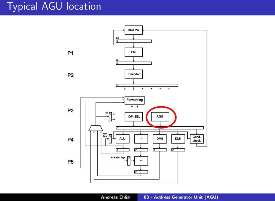
18 Basic AGU functionality Inputs Initial address Combinational output Address calculation logic circuit Keeper Address pointer Registered output Addressing feedback [Liu2008]

19 AGU Example Memory direct A <= Immediate data Address register + offset A <= AR + Immediate data Register indirect A <= RF Register + offset A <= RF + immediate data Addr. reg. post increment A <= AR; AR <= AR + 1 Addr. reg. pre decrement AR <= AR - 1;A <= AR; Address register + register A <= RF + AR

20 Modulo addressing Most general solution Address = TOP + AR % BUFFERSIZE Modulo operation too expensive in AGU (Unless BUFFERSIZE is a power of two) More practical: AR = AR + 1 If AR is more than BOT, correct by setting AR to TOP

21 AGU Example with Modulo Addressing Lets add Modulo addressing to the AGU: A=AR; AR = AR + 1 if(ar == BOT) AR = TOP;
22 AGU Example with Modulo Addressing What about post-decrement mode?
23 Modulo addressing - Post Decrement The programmer can exchange TOP and BOTTOM. Alternative - Add hardware to select TOP and BOTTOM based on which instruction is used
24 Variable step size Sometimes it makes sense to use a larger stepsize than 1 In this case we can t check for equality but must check for greater than or less than conditions if( AR > BOTTOM) AR = AR - BUFFERSIZE
25 Variable step size Keepers and registers for BUFFERSIZE, STEPSIZE, and BOTTOM not shown. Note that STEPSIZE can t be larger than BUFFERSIZE
26 Bit reversed addressing Important for FFT:s and similar creatures Typical behavior from FFT-like transforms: Input Transformed Output sample sample index (binary) x[0] X[0] 000 x[1] X[4] 100 x[2] X[2] 010 x[3] X[6] 110 x[4] X[1] 001 x[5] X[5] 101 x[6] X[3] 011 x[7] X[7] 111
27 Bit reversed addressing Case 1: Buffer size and buffer location can be fixed Case 2: Buffer size is fixed, buffer location is arbitrary Case 3: Buffer size and location are not fixed
28 Bit reversed addressing Case 1: Buffer size and buffer location can be fixed Solution: If buffer size is 2 N, place the start of the buffer at an even multiple of 2 N ADDR = {FIXED PART, BIT REVERSE(ADDR COUNTER N BITS);}
29 Bit reversed addressing Case 2: Buffer size is fixed, buffer location is arbitrary Solution: If buffer size is 2 N, place the start of the buffer at an even multiple of 2 N ADDR = BASE REGISTER + BIT REVERSE(ADDR COUNTER N BITS);
30 Bit reversed addressing Case 3: Buffer size and location are not fixed The most programmer friendly solution. Can be done in several ways.
31 Why design for memory hierarchy Small size memory is faster Acting data / program in small size memories Large size memory is area efficient Volume storage using large size memories
32 Typical SoC Memory Hierarchy DSP MCU Accelerators L1: RF DP+CP L1: RF DP+CP DP+CP DM1 DMn PM DM1 DMn PM DMn PM I/F DMA DMA I/F DMA I/F DMA SoCBUS and its arbitration / routing / control Main on chip memory Nonvolatile memory I/F Off chip DRAM I/F I/F [Liu2008]
33 Memory partition Requirements The number of data simultaneously Supporting access of different data types Memory shutting down for low power Overhead costs from memory peripheral Critical path from memory peripheral Limit of on chip memory size
34 Issues with off-chip memory Relatively low clockrate compared to on-chip Will need clock domain crossing, possibly using asynchronous FIFOs High latency Many clockcycles to send a command and receive a response Burst oriented Theoretical bandwidth can only be reached by relatively large consecutive read/write transactions
35 Why burst reads from external memory? Procedure for reading from (DDR-)SDRAM memory Read out one column (with around 2048 bits) from DRAM memory into flip-flops (slow) Do a burst read from these flip-flops (fast) Write back all bits into the DRAM memory Conclusion: If we have off-chip memory we should use burst reads if at all possible
36 Example: Image processing Typical organization of framebuffer memory Linear addresses
37 Example: Image processing Fetching an 8x8 pixel block from main memory Minimum transfer size: 16 pixels Minimum alignment: 16 pixels Must load: 256 bytes
38 Rearranging memory content to save bandwidth Use tile based frame buffer instead of linear
39 Rearranging memory content to save bandwidth Fetching 8x8 block from memory Minimum transfer size: 16 pixels Minimum alignment: 16 pixels Must load: 144 pixels Only 56% of the previous example!
40 Rearranging memory content to save bandwidth Extra important when using a wide memory bus and/or a cache
41 Buses External memory SDRAM, DDR-SDRAM, DDR2-SDRAM, etc SoC bus AMBA, PLB, Wishbone, etc You still need to worry about burst length, latency, etc
42 DMA definition and specification DMA: Direct memory access An external device independent of the core Running load and store in parallel with DSP DSP processor can do other things in parallel Requirements Large bandwidth and low latency Flexible and support different access patterns For DSP: Multiple access is not so important
43 Data memory access policies Both DMA and DSP can access the data memory simultaneously Requires a dual-port memory DSP has priority, DMA must use spare cycles to access DSP memory Verifying the DMA controller gets more complicated DMA has priority, can stall DSP processor Verifying the processor gets more complicated Ping-pong buffer Verifying the software gets more complicated
44 Ping-pong buffers
45 A simplified DMA architecture [Liu2008]
46 A typical DMA request Start address in data memory Start address in off-chip memory Length Priority Permission to stall DSP core Priority over other users of off-chip memory Interrupt flag Should the DSP core get an interrupt when the DMA is finished?
47 Scatter Gather-DMA Pointer to DMA request 1 Pointer to DMA request 2 Pointer to DMA request 3 End of List Start address in data memory Start address in off-chip memory Length Priority Permission stall DSP core Priority over other users of offchip memory Interrupt flag Should the DSP core get an interrupt when the DMA is finished?
48 Discussed on the whiteboard Why a cache takes more power than a scratch pad memory Schematic of a basic AGU including a control table Bit-reversed addressing in an AGU
1. Memory technology & Hierarchy
 1. Memory technology & Hierarchy RAM types Advances in Computer Architecture Andy D. Pimentel Memory wall Memory wall = divergence between CPU and RAM speed We can increase bandwidth by introducing concurrency
Modeling Sequential Elements with Verilog. Prof. Chien-Nan Liu TEL: 03-4227151 ext:34534 Email: [email protected]. Sequential Circuit
 Modeling Sequential Elements with Verilog Prof. Chien-Nan Liu TEL: 03-4227151 ext:34534 Email: [email protected] 4-1 Sequential Circuit Outputs are functions of inputs and present states of storage elements
What is a bus? A Bus is: Advantages of Buses. Disadvantage of Buses. Master versus Slave. The General Organization of a Bus
 Datorteknik F1 bild 1 What is a bus? Slow vehicle that many people ride together well, true... A bunch of wires... A is: a shared communication link a single set of wires used to connect multiple subsystems
Computer Systems Structure Main Memory Organization
 Computer Systems Structure Main Memory Organization Peripherals Computer Central Processing Unit Main Memory Computer Systems Interconnection Communication lines Input Output Ward 1 Ward 2 Storage/Memory
150127-Microprocessor & Assembly Language
 Chapter 3 Z80 Microprocessor Architecture The Z 80 is one of the most talented 8 bit microprocessors, and many microprocessor-based systems are designed around the Z80. The Z80 microprocessor needs an
7a. System-on-chip design and prototyping platforms
 7a. System-on-chip design and prototyping platforms Labros Bisdounis, Ph.D. Department of Computer and Communication Engineering 1 What is System-on-Chip (SoC)? System-on-chip is an integrated circuit
Architectures and Platforms
 Hardware/Software Codesign Arch&Platf. - 1 Architectures and Platforms 1. Architecture Selection: The Basic Trade-Offs 2. General Purpose vs. Application-Specific Processors 3. Processor Specialisation
361 Computer Architecture Lecture 14: Cache Memory
 1 361 Computer Architecture Lecture 14 Memory cache.1 The Motivation for s Memory System Processor DRAM Motivation Large memories (DRAM) are slow Small memories (SRAM) are fast Make the average access
ADVANCED PROCESSOR ARCHITECTURES AND MEMORY ORGANISATION Lesson-17: Memory organisation, and types of memory
 ADVANCED PROCESSOR ARCHITECTURES AND MEMORY ORGANISATION Lesson-17: Memory organisation, and types of memory 1 1. Memory Organisation 2 Random access model A memory-, a data byte, or a word, or a double
Computer Architecture
 Computer Architecture Random Access Memory Technologies 2015. április 2. Budapest Gábor Horváth associate professor BUTE Dept. Of Networked Systems and Services [email protected] 2 Storing data Possible
Chapter 1 Computer System Overview
 Operating Systems: Internals and Design Principles Chapter 1 Computer System Overview Eighth Edition By William Stallings Operating System Exploits the hardware resources of one or more processors Provides
Digitale Signalverarbeitung mit FPGA (DSF) Soft Core Prozessor NIOS II Stand Mai 2007. Jens Onno Krah
 Soft Core Prozessor NIOS II Stand Mai 2007. Jens Onno Krah") (DSF) Soft Core Prozessor NIOS II Stand Mai 2007 Jens Onno Krah Cologne University of Applied Sciences www.fh-koeln.de [email protected] NIOS II 1 1 What is Nios II? Altera s Second Generation
(DSF) Soft Core Prozessor NIOS II Stand Mai 2007 Jens Onno Krah Cologne University of Applied Sciences www.fh-koeln.de [email protected] NIOS II 1 1 What is Nios II? Altera s Second Generation
Lecture-3 MEMORY: Development of Memory:
 Lecture-3 MEMORY: It is a storage device. It stores program data and the results. There are two kind of memories; semiconductor memories & magnetic memories. Semiconductor memories are faster, smaller,
COMPUTER HARDWARE. Input- Output and Communication Memory Systems
 COMPUTER HARDWARE Input- Output and Communication Memory Systems Computer I/O I/O devices commonly found in Computer systems Keyboards Displays Printers Magnetic Drives Compact disk read only memory (CD-ROM)
Switch Fabric Implementation Using Shared Memory
 Order this document by /D Switch Fabric Implementation Using Shared Memory Prepared by: Lakshmi Mandyam and B. Kinney INTRODUCTION Whether it be for the World Wide Web or for an intra office network, today
Registers & Counters
 Objectives This section deals with some simple and useful sequential circuits. Its objectives are to: Introduce registers as multi-bit storage devices. Introduce counters by adding logic to registers implementing
DDR subsystem: Enhancing System Reliability and Yield
 DDR subsystem: Enhancing System Reliability and Yield Agenda Evolution of DDR SDRAM standards What is the variation problem? How DRAM standards tackle system variability What problems have been adequately
Homework # 2. Solutions. 4.1 What are the differences among sequential access, direct access, and random access?
 ECE337 / CS341, Fall 2005 Introduction to Computer Architecture and Organization Instructor: Victor Manuel Murray Herrera Date assigned: 09/19/05, 05:00 PM Due back: 09/30/05, 8:00 AM Homework # 2 Solutions
Agenda. Michele Taliercio, Il circuito Integrato, Novembre 2001
 Agenda Introduzione Il mercato Dal circuito integrato al System on a Chip (SoC) La progettazione di un SoC La tecnologia Una fabbrica di circuiti integrati 28 How to handle complexity G The engineering
ARM Microprocessor and ARM-Based Microcontrollers
 ARM Microprocessor and ARM-Based Microcontrollers Nguatem William 24th May 2006 A Microcontroller-Based Embedded System Roadmap 1 Introduction ARM ARM Basics 2 ARM Extensions Thumb Jazelle NEON & DSP Enhancement
Software based Finite State Machine (FSM) with general purpose processors
 with general purpose processors") Software based Finite State Machine (FSM) with general purpose processors White paper Joseph Yiu January 2013 Overview Finite state machines (FSM) are commonly used in electronic designs. FSM can be used
Software based Finite State Machine (FSM) with general purpose processors White paper Joseph Yiu January 2013 Overview Finite state machines (FSM) are commonly used in electronic designs. FSM can be used
Module 2. Embedded Processors and Memory. Version 2 EE IIT, Kharagpur 1
 Module 2 Embedded Processors and Memory Version 2 EE IIT, Kharagpur 1 Lesson 5 Memory-I Version 2 EE IIT, Kharagpur 2 Instructional Objectives After going through this lesson the student would Pre-Requisite
A New Paradigm for Synchronous State Machine Design in Verilog
 A New Paradigm for Synchronous State Machine Design in Verilog Randy Nuss Copyright 1999 Idea Consulting Introduction Synchronous State Machines are one of the most common building blocks in modern digital
Computers. Hardware. The Central Processing Unit (CPU) CMPT 125: Lecture 1: Understanding the Computer
 CMPT 125: Lecture 1: Understanding the Computer") Computers CMPT 125: Lecture 1: Understanding the Computer Tamara Smyth, [email protected] School of Computing Science, Simon Fraser University January 3, 2009 A computer performs 2 basic functions: 1.
Computers CMPT 125: Lecture 1: Understanding the Computer Tamara Smyth, [email protected] School of Computing Science, Simon Fraser University January 3, 2009 A computer performs 2 basic functions: 1.
Am186ER/Am188ER AMD Continues 16-bit Innovation
 Am186ER/Am188ER AMD Continues 16-bit Innovation 386-Class Performance, Enhanced System Integration, and Built-in SRAM Problem with External RAM All embedded systems require RAM Low density SRAM moving
Memory Systems. Static Random Access Memory (SRAM) Cell
 Cell") Memory Systems This chapter begins the discussion of memory systems from the implementation of a single bit. The architecture of memory chips is then constructed using arrays of bit implementations coupled
Memory Systems This chapter begins the discussion of memory systems from the implementation of a single bit. The architecture of memory chips is then constructed using arrays of bit implementations coupled
ADVANCED PROCESSOR ARCHITECTURES AND MEMORY ORGANISATION Lesson-12: ARM
 ADVANCED PROCESSOR ARCHITECTURES AND MEMORY ORGANISATION Lesson-12: ARM 1 The ARM architecture processors popular in Mobile phone systems 2 ARM Features ARM has 32-bit architecture but supports 16 bit
(Refer Slide Time: 00:01:16 min)
") Digital Computer Organization Prof. P. K. Biswas Department of Electronic & Electrical Communication Engineering Indian Institute of Technology, Kharagpur Lecture No. # 04 CPU Design: Tirning & Control
Digital Computer Organization Prof. P. K. Biswas Department of Electronic & Electrical Communication Engineering Indian Institute of Technology, Kharagpur Lecture No. # 04 CPU Design: Tirning & Control
Serial port interface for microcontroller embedded into integrated power meter
 Serial port interface for microcontroller embedded into integrated power meter Mr. Borisav Jovanović, Prof. dr. Predrag Petković, Prof. dr. Milunka Damnjanović, Faculty of Electronic Engineering Nis, Serbia
White Paper Utilizing Leveling Techniques in DDR3 SDRAM Memory Interfaces
 White Paper Introduction The DDR3 SDRAM memory architectures support higher bandwidths with bus rates of 600 Mbps to 1.6 Gbps (300 to 800 MHz), 1.5V operation for lower power, and higher densities of 2
EEM870 Embedded System and Experiment Lecture 1: SoC Design Overview
 EEM870 Embedded System and Experiment Lecture 1: SoC Design Overview Wen-Yen Lin, Ph.D. Department of Electrical Engineering Chang Gung University Email: [email protected] Feb. 2013 Course Overview
ETEC 2301 Programmable Logic Devices. Chapter 10 Counters. Shawnee State University Department of Industrial and Engineering Technologies
 ETEC 2301 Programmable Logic Devices Chapter 10 Counters Shawnee State University Department of Industrial and Engineering Technologies Copyright 2007 by Janna B. Gallaher Asynchronous Counter Operation
NAND Flash FAQ. Eureka Technology. apn5_87. NAND Flash FAQ
 What is NAND Flash? What is the major difference between NAND Flash and other Memory? Structural differences between NAND Flash and NOR Flash What does NAND Flash controller do? How to send command to
Computer Architecture
 Computer Architecture Slide Sets WS 2013/2014 Prof. Dr. Uwe Brinkschulte M.Sc. Benjamin Betting Part 11 Memory Management Computer Architecture Part 11 page 1 of 44 Prof. Dr. Uwe Brinkschulte, M.Sc. Benjamin
Advanced Computer Architecture-CS501. Computer Systems Design and Architecture 2.1, 2.2, 3.2
 Lecture Handout Computer Architecture Lecture No. 2 Reading Material Vincent P. Heuring&Harry F. Jordan Chapter 2,Chapter3 Computer Systems Design and Architecture 2.1, 2.2, 3.2 Summary 1) A taxonomy of
MICROPROCESSOR AND MICROCOMPUTER BASICS
 Introduction MICROPROCESSOR AND MICROCOMPUTER BASICS At present there are many types and sizes of computers available. These computers are designed and constructed based on digital and Integrated Circuit
How To Design A Single Chip System Bus (Amba) For A Single Threaded Microprocessor (Mma) (I386) (Mmb) (Microprocessor) (Ai) (Bower) (Dmi) (Dual
 For A Single Threaded Microprocessor (Mma) (I386) (Mmb) (Microprocessor) (Ai) (Bower) (Dmi) (Dual") Architetture di bus per System-On On-Chip Massimo Bocchi Corso di Architettura dei Sistemi Integrati A.A. 2002/2003 System-on on-chip motivations 400 300 200 100 0 19971999 2001 2003 2005 2007 2009 Transistors
Architetture di bus per System-On On-Chip Massimo Bocchi Corso di Architettura dei Sistemi Integrati A.A. 2002/2003 System-on on-chip motivations 400 300 200 100 0 19971999 2001 2003 2005 2007 2009 Transistors
Building Blocks for PRU Development
 Building Blocks for PRU Development Module 1 PRU Hardware Overview This session covers a hardware overview of the PRU-ICSS Subsystem. Author: Texas Instruments, Sitara ARM Processors Oct 2014 2 ARM SoC
Central Processing Unit (CPU)
") Central Processing Unit (CPU) CPU is the heart and brain It interprets and executes machine level instructions Controls data transfer from/to Main Memory (MM) and CPU Detects any errors In the following
Central Processing Unit (CPU) CPU is the heart and brain It interprets and executes machine level instructions Controls data transfer from/to Main Memory (MM) and CPU Detects any errors In the following
Memory Basics. SRAM/DRAM Basics
 Memory Basics RAM: Random Access Memory historically defined as memory array with individual bit access refers to memory with both Read and Write capabilities ROM: Read Only Memory no capabilities for
Chapter 7. Registers & Register Transfers. J.J. Shann. J. J. Shann
 Chapter 7 Registers & Register Transfers J. J. Shann J.J. Shann Chapter Overview 7- Registers and Load Enable 7-2 Register Transfers 7-3 Register Transfer Operations 7-4 A Note for VHDL and Verilog Users
SoC IP Interfaces and Infrastructure A Hybrid Approach
 SoC IP Interfaces and Infrastructure A Hybrid Approach Cary Robins, Shannon Hill ChipWrights, Inc. ABSTRACT System-On-Chip (SoC) designs incorporate more and more Intellectual Property (IP) with each year.
Low Power AMD Athlon 64 and AMD Opteron Processors
 Low Power AMD Athlon 64 and AMD Opteron Processors Hot Chips 2004 Presenter: Marius Evers Block Diagram of AMD Athlon 64 and AMD Opteron Based on AMD s 8 th generation architecture AMD Athlon 64 and AMD
Pre-tested System-on-Chip Design. Accelerates PLD Development
 Pre-tested System-on-Chip Design Accelerates PLD Development March 2010 Lattice Semiconductor 5555 Northeast Moore Ct. Hillsboro, Oregon 97124 USA Telephone: (503) 268-8000 www.latticesemi.com 1 Pre-tested
Computer-System Architecture
 Chapter 2: Computer-System Structures Computer System Operation I/O Structure Storage Structure Storage Hierarchy Hardware Protection General System Architecture 2.1 Computer-System Architecture 2.2 Computer-System
MP3 Player CSEE 4840 SPRING 2010 PROJECT DESIGN. [email protected]. [email protected]
 MP3 Player CSEE 4840 SPRING 2010 PROJECT DESIGN Zheng Lai Zhao Liu Meng Li Quan Yuan [email protected] [email protected] [email protected] [email protected] I. Overview Architecture The purpose
SOLVING HIGH-SPEED MEMORY INTERFACE CHALLENGES WITH LOW-COST FPGAS
 SOLVING HIGH-SPEED MEMORY INTERFACE CHALLENGES WITH LOW-COST FPGAS A Lattice Semiconductor White Paper May 2005 Lattice Semiconductor 5555 Northeast Moore Ct. Hillsboro, Oregon 97124 USA Telephone: (503)
Von der Hardware zur Software in FPGAs mit Embedded Prozessoren. Alexander Hahn Senior Field Application Engineer Lattice Semiconductor
 Von der Hardware zur Software in FPGAs mit Embedded Prozessoren Alexander Hahn Senior Field Application Engineer Lattice Semiconductor AGENDA Overview Mico32 Embedded Processor Development Tool Chain HW/SW
Ingar Fredriksen AVR Applications Manager. Tromsø August 12, 2005
 Ingar Fredriksen AVR Applications Manager Tromsø August 12, 2005 Atmel Norway 2005 Atmel Norway 2005 The history of computers Foundation for modern computing 3 An automatic computing machine must have:
A Verilog HDL Test Bench Primer Application Note
 A Verilog HDL Test Bench Primer Application Note Table of Contents Introduction...1 Overview...1 The Device Under Test (D.U.T.)...1 The Test Bench...1 Instantiations...2 Figure 1- DUT Instantiation...2
CHAPTER 7: The CPU and Memory
 CHAPTER 7: The CPU and Memory The Architecture of Computer Hardware, Systems Software & Networking: An Information Technology Approach 4th Edition, Irv Englander John Wiley and Sons 2010 PowerPoint slides
Navigating Big Data with High-Throughput, Energy-Efficient Data Partitioning
 Application-Specific Architecture Navigating Big Data with High-Throughput, Energy-Efficient Data Partitioning Lisa Wu, R.J. Barker, Martha Kim, and Ken Ross Columbia University Xiaowei Wang Rui Chen Outline
Slide Set 8. for ENCM 369 Winter 2015 Lecture Section 01. Steve Norman, PhD, PEng
 Slide Set 8 for ENCM 369 Winter 2015 Lecture Section 01 Steve Norman, PhD, PEng Electrical & Computer Engineering Schulich School of Engineering University of Calgary Winter Term, 2015 ENCM 369 W15 Section
Chapter 11 I/O Management and Disk Scheduling
 Operating Systems: Internals and Design Principles, 6/E William Stallings Chapter 11 I/O Management and Disk Scheduling Dave Bremer Otago Polytechnic, NZ 2008, Prentice Hall I/O Devices Roadmap Organization
Modeling Registers and Counters
 Lab Workbook Introduction When several flip-flops are grouped together, with a common clock, to hold related information the resulting circuit is called a register. Just like flip-flops, registers may
A3 Computer Architecture
 A3 Computer Architecture Engineering Science 3rd year A3 Lectures Prof David Murray [email protected] www.robots.ox.ac.uk/ dwm/courses/3co Michaelmas 2000 1 / 1 6. Stacks, Subroutines, and Memory
Chapter 2 Basic Structure of Computers. Jin-Fu Li Department of Electrical Engineering National Central University Jungli, Taiwan
 Chapter 2 Basic Structure of Computers Jin-Fu Li Department of Electrical Engineering National Central University Jungli, Taiwan Outline Functional Units Basic Operational Concepts Bus Structures Software
Intel 965 Express Chipset Family Memory Technology and Configuration Guide
 Intel 965 Express Chipset Family Memory Technology and Configuration Guide White Paper - For the Intel 82Q965, 82Q963, 82G965 Graphics and Memory Controller Hub (GMCH) and Intel 82P965 Memory Controller
16-bit ALU, Register File and Memory Write Interface
 CS M152B Fall 2002 Project 2 16-bit ALU, Register File and Memory Write Interface Suggested Due Date: Monday, October 21, 2002 Actual Due Date determined by your Lab TA This project will take much longer
Keil C51 Cross Compiler
 Keil C51 Cross Compiler ANSI C Compiler Generates fast compact code for the 8051 and it s derivatives Advantages of C over Assembler Do not need to know the microcontroller instruction set Register allocation
Enhancing High-Speed Telecommunications Networks with FEC
 White Paper Enhancing High-Speed Telecommunications Networks with FEC As the demand for high-bandwidth telecommunications channels increases, service providers and equipment manufacturers must deliver
Switched Interconnect for System-on-a-Chip Designs
 witched Interconnect for ystem-on-a-chip Designs Abstract Daniel iklund and Dake Liu Dept. of Physics and Measurement Technology Linköping University -581 83 Linköping {danwi,dake}@ifm.liu.se ith the increased
Price/performance Modern Memory Hierarchy
 Lecture 21: Storage Administration Take QUIZ 15 over P&H 6.1-4, 6.8-9 before 11:59pm today Project: Cache Simulator, Due April 29, 2010 NEW OFFICE HOUR TIME: Tuesday 1-2, McKinley Last Time Exam discussion
DEPARTMENT OF COMPUTER SCIENCE & ENGINEERING Question Bank Subject Name: EC6504 - Microprocessor & Microcontroller Year/Sem : II/IV
 DEPARTMENT OF COMPUTER SCIENCE & ENGINEERING Question Bank Subject Name: EC6504 - Microprocessor & Microcontroller Year/Sem : II/IV UNIT I THE 8086 MICROPROCESSOR 1. What is the purpose of segment registers
ARM Webinar series. ARM Based SoC. Abey Thomas
 ARM Webinar series ARM Based SoC Verification Abey Thomas Agenda About ARM and ARM IP ARM based SoC Verification challenges Verification planning and strategy IP Connectivity verification Performance verification
Testing of Digital System-on- Chip (SoC)
") Testing of Digital System-on- Chip (SoC) 1 Outline of the Talk Introduction to system-on-chip (SoC) design Approaches to SoC design SoC test requirements and challenges Core test wrapper P1500 core test
Testing of Digital System-on- Chip (SoC) 1 Outline of the Talk Introduction to system-on-chip (SoC) design Approaches to SoC design SoC test requirements and challenges Core test wrapper P1500 core test
Chapter 2 Logic Gates and Introduction to Computer Architecture
 Chapter 2 Logic Gates and Introduction to Computer Architecture 2.1 Introduction The basic components of an Integrated Circuit (IC) is logic gates which made of transistors, in digital system there are
MICROPROCESSOR. Exclusive for IACE Students www.iace.co.in iacehyd.blogspot.in Ph: 9700077455/422 Page 1
 MICROPROCESSOR A microprocessor incorporates the functions of a computer s central processing unit (CPU) on a single Integrated (IC), or at most a few integrated circuit. It is a multipurpose, programmable
Tensilica Software Development Toolkit (SDK)
") Tensilica Datasheet Tensilica Software Development Toolkit (SDK) Quickly develop application code Features Cadence Tensilica Xtensa Xplorer Integrated Development Environment (IDE) with full graphical
Tensilica Datasheet Tensilica Software Development Toolkit (SDK) Quickly develop application code Features Cadence Tensilica Xtensa Xplorer Integrated Development Environment (IDE) with full graphical
ECE410 Design Project Spring 2008 Design and Characterization of a CMOS 8-bit Microprocessor Data Path
 ECE410 Design Project Spring 2008 Design and Characterization of a CMOS 8-bit Microprocessor Data Path Project Summary This project involves the schematic and layout design of an 8-bit microprocessor data
ESP-CV Custom Design Formal Equivalence Checking Based on Symbolic Simulation
 Datasheet -CV Custom Design Formal Equivalence Checking Based on Symbolic Simulation Overview -CV is an equivalence checker for full custom designs. It enables efficient comparison of a reference design
Introduction to System-on-Chip
 Introduction to System-on-Chip COE838: Systems-on-Chip Design http://www.ee.ryerson.ca/~courses/coe838/ Dr. Gul N. Khan http://www.ee.ryerson.ca/~gnkhan Electrical and Computer Engineering Ryerson University
Technical Note. Micron NAND Flash Controller via Xilinx Spartan -3 FPGA. Overview. TN-29-06: NAND Flash Controller on Spartan-3 Overview
 Technical Note TN-29-06: NAND Flash Controller on Spartan-3 Overview Micron NAND Flash Controller via Xilinx Spartan -3 FPGA Overview As mobile product capabilities continue to expand, so does the demand
Counters and Decoders
 Physics 3330 Experiment #10 Fall 1999 Purpose Counters and Decoders In this experiment, you will design and construct a 4-bit ripple-through decade counter with a decimal read-out display. Such a counter
SYSTEM-ON-PROGRAMMABLE-CHIP DESIGN USING A UNIFIED DEVELOPMENT ENVIRONMENT. Nicholas Wieder
 SYSTEM-ON-PROGRAMMABLE-CHIP DESIGN USING A UNIFIED DEVELOPMENT ENVIRONMENT by Nicholas Wieder A thesis submitted to the faculty of The University of North Carolina at Charlotte in partial fulfillment of
Let s put together a Manual Processor
 Lecture 14 Let s put together a Manual Processor Hardware Lecture 14 Slide 1 The processor Inside every computer there is at least one processor which can take an instruction, some operands and produce
Avalon Interface Specifications
 Avalon Interface Specifications Subscribe MNL-AVABUSREF 101 Innovation Drive San Jose, CA 95134 www.altera.com TOC-2 Contents 1. Introduction to the Avalon Interface Specifications... 1-1 1.1 Avalon Properties
Lecture 5: Gate Logic Logic Optimization
 Lecture 5: Gate Logic Logic Optimization MAH, AEN EE271 Lecture 5 1 Overview Reading McCluskey, Logic Design Principles- or any text in boolean algebra Introduction We could design at the level of irsim
OC By Arsene Fansi T. POLIMI 2008 1
 IBM POWER 6 MICROPROCESSOR OC By Arsene Fansi T. POLIMI 2008 1 WHAT S IBM POWER 6 MICROPOCESSOR The IBM POWER6 microprocessor powers the new IBM i-series* and p-series* systems. It s based on IBM POWER5
A New Chapter for System Designs Using NAND Flash Memory
 A New Chapter for System Designs Using Memory Jim Cooke Senior Technical Marketing Manager Micron Technology, Inc December 27, 2010 Trends and Complexities trends have been on the rise since was first
Chapter 5 :: Memory and Logic Arrays
 Chapter 5 :: Memory and Logic Arrays Digital Design and Computer Architecture David Money Harris and Sarah L. Harris Copyright 2007 Elsevier 5- ROM Storage Copyright 2007 Elsevier 5- ROM Logic Data
EE482: Advanced Computer Organization Lecture #11 Processor Architecture Stanford University Wednesday, 31 May 2000. ILP Execution
 EE482: Advanced Computer Organization Lecture #11 Processor Architecture Stanford University Wednesday, 31 May 2000 Lecture #11: Wednesday, 3 May 2000 Lecturer: Ben Serebrin Scribe: Dean Liu ILP Execution
We r e going to play Final (exam) Jeopardy! "Answers:" "Questions:" - 1 -
 Jeopardy! Answers: Questions: - 1 -") . (0 pts) We re going to play Final (exam) Jeopardy! Associate the following answers with the appropriate question. (You are given the "answers": Pick the "question" that goes best with each "answer".)
. (0 pts) We re going to play Final (exam) Jeopardy! Associate the following answers with the appropriate question. (You are given the "answers": Pick the "question" that goes best with each "answer".)
GETTING STARTED WITH PROGRAMMABLE LOGIC DEVICES, THE 16V8 AND 20V8
 GETTING STARTED WITH PROGRAMMABLE LOGIC DEVICES, THE 16V8 AND 20V8 Robert G. Brown All Rights Reserved August 25, 2000 Alta Engineering 58 Cedar Lane New Hartford, CT 06057-2905 (860) 489-8003 www.alta-engineering.com
Design of a High Speed Communications Link Using Field Programmable Gate Arrays
 Customer-Authored Application Note AC103 Design of a High Speed Communications Link Using Field Programmable Gate Arrays Amy Lovelace, Technical Staff Engineer Alcatel Network Systems Introduction A communication
what operations can it perform? how does it perform them? on what kind of data? where are instructions and data stored?
 Inside the CPU how does the CPU work? what operations can it perform? how does it perform them? on what kind of data? where are instructions and data stored? some short, boring programs to illustrate the
CHAPTER 2: HARDWARE BASICS: INSIDE THE BOX
 CHAPTER 2: HARDWARE BASICS: INSIDE THE BOX Multiple Choice: 1. Processing information involves: A. accepting information from the outside world. B. communication with another computer. C. performing arithmetic
Applying the Benefits of Network on a Chip Architecture to FPGA System Design
 Applying the Benefits of on a Chip Architecture to FPGA System Design WP-01149-1.1 White Paper This document describes the advantages of network on a chip (NoC) architecture in Altera FPGA system design.
Logical Operations. Control Unit. Contents. Arithmetic Operations. Objectives. The Central Processing Unit: Arithmetic / Logic Unit.
 Objectives The Central Processing Unit: What Goes on Inside the Computer Chapter 4 Identify the components of the central processing unit and how they work together and interact with memory Describe how
Introduction Disks RAID Tertiary storage. Mass Storage. CMSC 412, University of Maryland. Guest lecturer: David Hovemeyer.
 Guest lecturer: David Hovemeyer November 15, 2004 The memory hierarchy Red = Level Access time Capacity Features Registers nanoseconds 100s of bytes fixed Cache nanoseconds 1-2 MB fixed RAM nanoseconds
Computer Architecture Lecture 2: Instruction Set Principles (Appendix A) Chih Wei Liu 劉 志 尉 National Chiao Tung University [email protected].
 Chih Wei Liu 劉 志 尉 National Chiao Tung University cwliu@twins.ee.nctu.edu.") Computer Architecture Lecture 2: Instruction Set Principles (Appendix A) Chih Wei Liu 劉 志 尉 National Chiao Tung University [email protected] Review Computers in mid 50 s Hardware was expensive
Computer Architecture Lecture 2: Instruction Set Principles (Appendix A) Chih Wei Liu 劉 志 尉 National Chiao Tung University [email protected] Review Computers in mid 50 s Hardware was expensive
SDLC Controller. Documentation. Design File Formats. Verification
 January 15, 2004 Product Specification 11 Stonewall Court Woodcliff Lake, NJ 07677 USA Phone: +1-201-391-8300 Fax: +1-201-391-8694 E-mail: [email protected] URL: www.cast-inc.com Features AllianceCORE
Lizy Kurian John Electrical and Computer Engineering Department, The University of Texas as Austin
 BUS ARCHITECTURES Lizy Kurian John Electrical and Computer Engineering Department, The University of Texas as Austin Keywords: Bus standards, PCI bus, ISA bus, Bus protocols, Serial Buses, USB, IEEE 1394
With respect to the way of data access we can classify memories as:
 Memory Classification With respect to the way of data access we can classify memories as: - random access memories (RAM), - sequentially accessible memory (SAM), - direct access memory (DAM), - contents
The Central Processing Unit:
 The Central Processing Unit: What Goes on Inside the Computer Chapter 4 Objectives Identify the components of the central processing unit and how they work together and interact with memory Describe how
AN 223: PCI-to-DDR SDRAM Reference Design
 AN 223: PCI-to-DDR SDRAM Reference Design May 2003, ver. 1.0 Application Note 223 Introduction The Altera PCI-to-DDR SDRAM reference design, which you can download to the Stratix PCI development board,
Computer Systems Structure Input/Output
 Computer Systems Structure Input/Output Peripherals Computer Central Processing Unit Main Memory Computer Systems Interconnection Communication lines Input Output Ward 1 Ward 2 Examples of I/O Devices
Exception and Interrupt Handling in ARM
 Exception and Interrupt Handling in ARM Architectures and Design Methods for Embedded Systems Summer Semester 2006 Author: Ahmed Fathy Mohammed Abdelrazek Advisor: Dominik Lücke Abstract We discuss exceptions
Introduction to Digital System Design
 Introduction to Digital System Design Chapter 1 1 Outline 1. Why Digital? 2. Device Technologies 3. System Representation 4. Abstraction 5. Development Tasks 6. Development Flow Chapter 1 2 1. Why Digital