Probe Needle Wear and Contact Resistance
|
|
|
- Ira Wheeler
- 9 years ago
- Views:
Transcription
1 Probe Needle Wear and Contact Resistance Jerry J. Broz, Ph.D. Research and Development Advanced Probing Systems, Inc. Boulder, Colorado Reynaldo M. Rincon Probe Coordinator Texas Instruments, Inc. Dallas, Texas 1

2 Participants SEMATECH Probes PTAB Probe Needles Advanced Probing Systems, Inc. Probe Cards CerProbe Corporation JEM America Micro-Probe, Inc. Probe Technology Corporation Wentworth Laboratories Testing Facilities Applied Precision, Inc. (John Strom, Kenneth Sokol, Bryce Ekstrom) Sandia National Laboratories (David Monroe, Scot Swanson) 2

3 No Benchmarking Research Objectives Probe card construction was specified for this study Overall performance between cards WAS NOT compared Quantify abrasive cleaning effects Probe tip wear due to burnishing Appropriate cleaning procedures Evaluate probe needle wear behavior Room and elevated temperature touchdown testing Appropriate probe needle metal system 3

4 Research Focus SEMATECH 1997 Development Roadmap Room temperature (hot chuck at 30 o C) Elevated temperature (hot chuck at 85 o C) Practice for probe card cleaning 3-µm grit burnishing pad (hot chuck at 30 o C) Practices used for 70 µm pitch probe cards Tungsten and tungsten-rhenium probe materials and diameter probe needles Three-tiered epoxy ring probe cards For this presentation only Tier 1 behavior will be discussed 4

5 Testing Environments Abrasive cleaning Room temperature(30 o C) High temperature (85 o C) Low forcing current (50 ma) Probe Needles Focus on Primary Probe Needle Properties Material Probe and probe tip diameter Etch length 5

6 Probe Card Consistent Secondary Probe Needle Variables Balanced contact force Overtravel Beam angle Tip angle Etc. 6

7 Probe Needle Specifications Isolinear Probe Needles Known probe tip geometry Tip diameter and length mathematically related Probe Needle 5-mil Diameter Etch Length (inch) Etch Rate (deg) Finish Tungsten (W): Matte Tungsten-Rhenium (WRe): Polish 7-mil Diameter Tungsten (W): Matte Tungsten-Rhenium (WRe): Polish 7
: Matte Tungsten-Rhenium (WRe): Polish 7-mil Diameter 0.090 0.100 0.")
8 Probe Card Specifications Board Style: HP 4062, 4" PCB Probe Depth: 150 mils Test Temperature: 25 o to 85 o C Ring Material: Ceramic Tip Diameter: 1.2 ± 0.1 mils Overdrive: 3 mils Tip Shape: Flat Planarity: ± 0.5 mils Tip Angle:. 103 ± 3 deg. Alignment: ± 0.5 mils Beam Angle: 10 deg. Leakage: 100 na Pad Material: Aluminum Contact Resistance 1.5 to 2.0 Ω Fanout: 0 ± 3 deg. Gram Force: 2 grams/mil BCF: ± 20% 8

9 60-Pin Configuration Tungsten 5-mil diameter 1400 Y - Location (µm) Tungsten 7-mil diameter TIER 1 TIER 2 TIER 3 Tungsten-Rhenium 7-mil diameter Tungsten-Rhenium 5-mil diameter X - Location (µm) 9

10 Probe Card 10

11 Abrasive Testing Test Wafers 6-inch scrap metallized wafer 3-µm abrasive pad, i.e. the pink stuff Touchdown Testing 8-inch metallized wafer manufactured by SEMATECH Titanium-nitride substrate 1-µm thick Aluminum layer 11

12 Stepping Pattern 12

13 Test Equipment ElectroGlas-4080 Tester with Hot Chuck Burnishing pad touchdown testing Metallized wafer touchdown testing at 30 o C and 85 o C HP4062 Parametric 48-Channel Analyzer On-line contact resistance measurements Applied Precision PRVX 2 -Probe Card Analyzer Probe tip diameter Contact resistance Balanced contact force 13

14 Touchdown Test Flow 3-µm Abrasive Pad 3.0-mil overtravel, linear mode, double-touchdown mode PRVX 2 metrology performed after 0, 7.5K, and 15K touchdowns Contact resistance Tip diameter Metallized Wafer at 30 o and 85 o C 3.0 mil overdrive, double-touchdown mode (8 touchdowns/second) Contact resistance measurements every 5K touchdowns PRVX 2 metrology performed after 0, 250K, and 500K touchdowns Contact resistance Tip diameter 14
 Contact resistance measurements every 5K")
15 3-µm Abrasive Pad 15
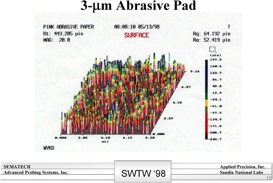
16 3-µm Abrasive Pad Tungsten vs. Tungsten-Rhenium Abrasive particles are considerably harder than both probe materials No significant differences between materials in amount of tip length removed 5-mil vs. 7-mil Diameter Probe Needles Amount of tip length removed from the 5-mil probes was greater than that of the 7-mil probes Contact Resistance Measurements Baseline ( as delivered ) and post-touchdown C RES values were higher than expected Cleaning was performed and C RES values were considerably reduced Contamination on probe tip surface - tungsten-oxide? other residue? 16

17 3-µm Abrasive Pad Approximate Wear Rates Changes in tip geometry occur with each touchdown Wear rate = f(overtravel, scrub length, BCF, etch length, contact materials) Conservative first approximation of abrasive wear rates Estimated amount of material removed 0 to 7.5K Estimated amount of material removed 0 to 15K 5-mil diameter 38 Å per touchdown 52 Å per touchdown 7-mil diameter 35 Å per touchdown 48 Å per touchdown 17

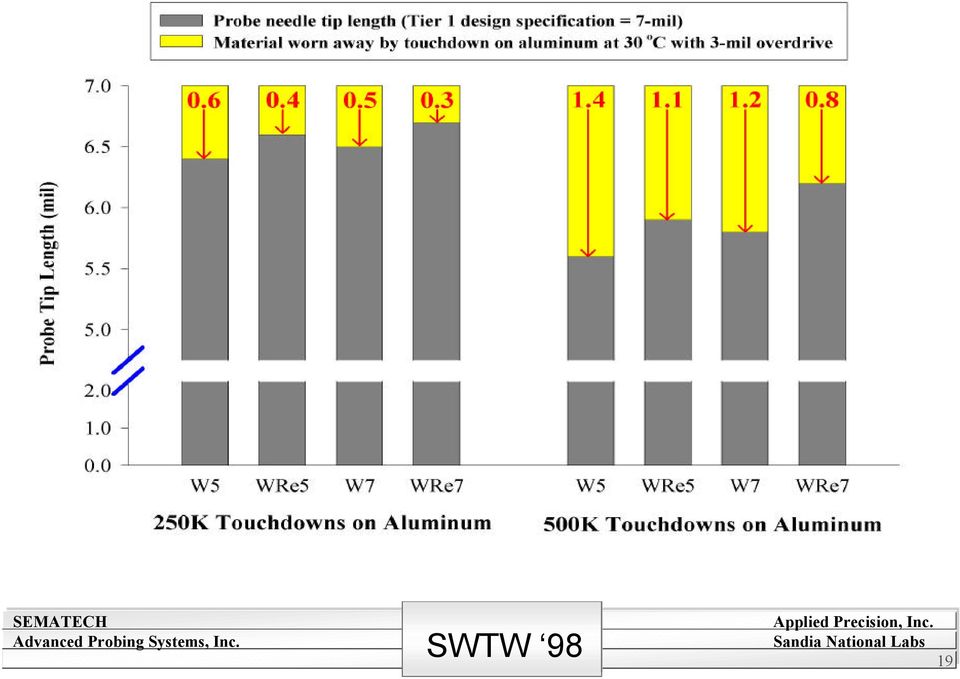
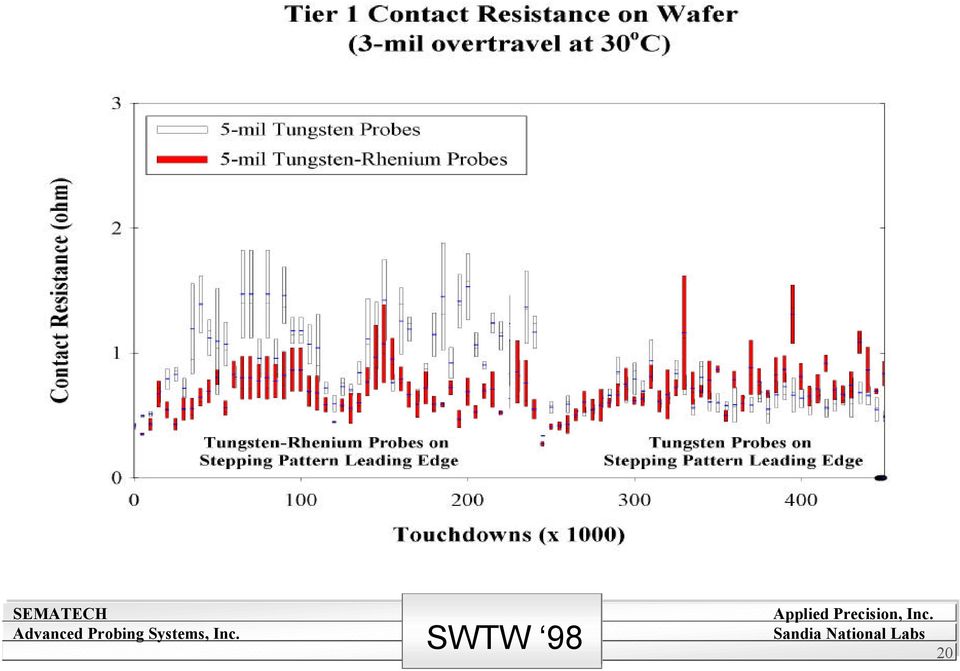
18 Al-Wafer at 30 o and 85 o C Probe Tip Wear Characteristics Isolinear taper shape was used to calculate average tip length changes Contact Resistance Box plots were used to show the range and mean of C RES values for material 18

19 19
20 20
21 21
22 Al-Wafer at 30 o C Wear and C RES 7-mil WRe-probes demonstrated significantly lower C RES values than 7- mil W-probes Differences between the 5-mil probes were not as significant Microhardness values of the probes W005 WRe005 W007 WRe007 VHN (kg/mm 2 ) 738 ± ± ± ± 23 C RES on Virgin vs. Scrubbed Aluminum C RES response of the WRe-probes unaffected by wafer surface condition On the other hand, the W-probes demonstrated marked differences 22
23 23
24 24
25 25
26 Al-Wafer at 85 o C Wear and C RES Reductions in WRe-probe tip lengths were significantly less than those of the W-probes Overall, the WRe-probes demonstrated lower and more stable C RES behavior Temperature Effects Metallurgical fact - materials soften with increased temperature Rhenium stabilizes small diameter wire grain structure at high temperatures Grain structure affects hardness and wear characteristics of probe needles The softening rate of WRe-probes differs from than that of W-probes 26
27 Application of Results A Thought Experiment Probe card required to test 500K die Testing performed at room and high temperature Triple Hit cleaning every 100 die 7.5K cleaning touchdowns after 250K die 15K cleaning touchdowns after 500K die Can an estimate be made of the probe service life? Reduction in tip length Increase in tip diameter 27
28 28
29 29
30 Summary TIER 1 ONLY No Benchmarking Probe Needle Wear Abrasive Cleaning Cleaning pad material is dramatically harder than both probe materials No significant differences in the amount of tip length removed Wear rate first approximations based on 15K cleanings: 52 and 48 Å per touchdown for 5-mil and 7-mil probes, respectively Wear rate = f(overtravel, scrub length, BCF, etch length, contact materials) 30
31 Probe Needle Wear Aluminum-wafer at 30 o C Summary Difference in wear behavior were observed for the 7-mil probes and not as severe for the 5-mil probes Wear rate first approximations based on 500K touchdowns: 700, 560, 600, and 380 Å per 1K-touchdowns for W005, WRe005, W007, and WRe007, respectively Hardness values of the 7-mil WRe-probes were significantly higher than those of the W-probes The 5-mil probes had comparable hardness values and hence demonstrated similar wear characteristics As the diameter of the probe needles decreases, the hardness of tungsten and tungsten-rhenium become similar 31
32 Probe Needle Wear Al-Wafer at 85 o C Summary Wear differences were exacerbated by the higher temperature Wear rate first approximations based on 500K touchdowns: 1100, 700, 900, and 560 Å per 1K-touchdowns for W005, WRe005, W007, and WRe007, respectively Increased temperature results in a thicker Al-oxide layer and a reduction in the probe needle hardness Changes of the WRe-probe tip lengths were significantly less than those of the W-probes Alloying with rhenium stabilizes the grain structure and hardness at high temperatures The temperature dependent softening of WRe-probes is different than that of W-probes 32
33 Contact Resistance Al-Wafer at 30 o C Summary C RES consistency of the W-probes was affected by the wafer surface condition W-probes demonstrated higher C RES values on the scrubbed portion WRe-probes demonstrated consistent C RES values regardless of the wafer surface, i.e. virgin vs. scrubbed Al-Wafer at 85 o C C RES variance of all probe needles was greater at higher temperature C RES consistency of the W-probes was affected by the wafer surface condition; but not as dramatically as at room temperature C RES behavior of the WRe-probes was unaffected by the wafer surface condition Overall, the WRe-probes demonstrated lower and consistent C RES values 33
34 Summary Probe Service Life Estimates First approximations of the service life for Tier 1 were made Differences in probe tip wear are over-shadowed by abrasive cleaning Service Life = f(temperature, current, overtravel, scrub length, BCF, cleaning frequency, and contact material) The results indicate that WRe-probes would provide a longer service life than W-probes at high temperatures Benefits of Tungsten-Rhenium At room temperature, WRe-probes provide C RES consistency with slight improvements in wear that over-shadowed by abrasive cleaning At high temperature, WRe-probes provide C RES consistency and significant improvements in wear 34
35 Additional Observations Side Bar C RES values of probes that never touched a wafer were higher than expected Cleaning was performed and C RES values were considerably reduced Contamination on probe tip surface - tungsten-oxide? other residue? who really knows? Future Work Analysis of Tier 2 and Tier 3 behavior 35
Low and Stable Contact Resistance With Reduced Cleaning......A Paradigm Shift
 Low and Stable Contact Resistance With Reduced Cleaning......A Paradigm Shift Jerry J. Broz, Ph.D. Research and Development Boulder, Colorado Reynaldo M. Rincon Probe Coordinator, Inc. Dallas, Texas 1
Comprehensive Approach to Control Contact Resistance Instability and Improve First Pass Yield of Bumped Devices
 Comprehensive Approach to Control Contact Resistance Instability and Improve First Pass Yield of Bumped Devices Atsushi Mine Phill Mai JEM 3000 Laurelview Court Fremont, CA 94538 Joe Foerstel Sean Chen
Vertical Probe Alternative for Cantilever Pad Probing
 Robert Doherty Analog Devices, Inc. Robert Rogers Wentworth Laboratories, Inc. Vertical Probe Alternative for Cantilever Pad Probing June 8-11, 8 2008 San Diego, CA USA Introduction This presentation summarizes
Wafer Placement Repeatibility and Robot Speed Improvements for Bonded Wafer Pairs Used in 3D Integration
 Wafer Placement Repeatibility and Robot Speed Improvements for Bonded Wafer Pairs Used in 3D Integration Andrew C. Rudack 3D Interconnect Metrology and Standards SEMATECH Albany, NY [email protected]
Lapping and Polishing Basics
 Lapping and Polishing Basics Applications Laboratory Report 54 Lapping and Polishing 1.0: Introduction Lapping and polishing is a process by which material is precisely removed from a workpiece (or specimen)
TechCut 4 Precision Low Speed Saw
 Product Brochure TechCut 4 Precision Low Speed Saw 3" - 6" Blade Range Digital Speed Display 1-Micron Sample Indexing Spring-Loaded Dressing Stick Attachment All Aluminum & Stainless Steel Construction
1.Introduction. Introduction. Most of slides come from Semiconductor Manufacturing Technology by Michael Quirk and Julian Serda.
 .Introduction If the automobile had followed the same development cycle as the computer, a Rolls- Royce would today cost $00, get one million miles to the gallon and explode once a year Most of slides
Right Angle Grinder USA MADE FLAP DISCS
 USA MADE FLAP DISC Right Angle Grinder CGW Offers the Most Extensive Line of Flap Discs in the Marketplace CGW flap discs blend and finish in one operation which replaces the traditional twostep grinding
3.8 HSP (High Solids Polyurethane)
") Description is a single-stage topcoat designed for commercial and automotive refinishing. This product provides Superior UV durability as well as commercial grade chemical resistance. 3.8 HSP has excellent
Description is a single-stage topcoat designed for commercial and automotive refinishing. This product provides Superior UV durability as well as commercial grade chemical resistance. 3.8 HSP has excellent
Choosing a Stencil. By William E. Coleman, Ph.D. and Michael R. Burgess
 Choosing a Stencil Is a stencil a commodity or a precision tool? A commodity is something that can be purchased from many suppliers, with the expectation that the performance will be the same. A precision
Tableting Punch Performance Can Be Improved With Precision Coatings
 Tableting Punch Performance Can Be Improved With Precision Coatings by Arnold H. Deutchman, Ph. D. Director of Research and Development (614) 873-4529 X 114 [email protected] Mr. Dale C. Natoli
Survival Laser SL-001BB Laser Parts Bundle Assembly & Operation Instructions
 Survival Laser SL-001BB Laser Parts Bundle Assembly & Operation Instructions WARNING: READ ALL INSTRUCTIONS AND THE ENCLOSED SAFETY PRECAUTIONS BEFORE ASSEMBLY AND USE Assemble and use these parts ONLY
Screen Melts. Introduction. Selecting Screen Material. Prefire Before Using. Spalling. Kiln Shelf
 Introduction There are two terrific reasons for melting glass through screens. First because screen melts produce uniquely intricate patterns not possible any other way and second because it does it using
FABRICATION 2011 SERVICES TECHNOLOGIES CAPABILITIES INDUSTRY
 FABRICATION 2011 SERVICES 24HRS - 5 DAYS ON QUICK TURN PROTOTYPE Dear Customer, We would like to take this opportunity to welcome you and thank you for looking to ASA PCB as your Printed Circuit Manufacturing
RC Scrub R. High Performance Test Socket Systems for Micro Lead Frame Packages
 RC Scrub R High Performance Test Socket Systems for Micro Lead Frame Packages Abstract RC Scrub R ATE test sockets from Ardent Concepts provide excellent AC performance, long lifecycle/durability, and
Dynamic & Proto Circuits Inc. Corporate Presentation
 Dynamic & Proto Circuits Inc. Corporate Presentation 1 DAPC Facility 54,000 Sq.ft./6,000 Sq.M 2 Multilayer Process 3 Solder Mask Options BLUE BLACK RED GREEN DRY FILM CLEAR 4 Investing in Technology New
Card electrical characteristic, Parallelism & Reliability. Jung Keun Park Willtechnology
 Description of the MEMS CIS Probe Card electrical characteristic, Parallelism & Reliability Jung Keun Park Willtechnology Background Overview Design limitation, Things to consider, Trend CIS Probe Card
Wafer Level Testing Challenges for Flip Chip and Wafer Level Packages
 Wafer Level Testing Challenges for Flip Chip and Wafer Level Packages by Lim Kok Hwa and Andy Chee STATS ChipPAC Ltd. 5 Yishun Street 23, Singapore 768442 [email protected]; [email protected]
COATED CARBIDE. TiN. Al 2 O 3
 COATED CARBIDE GENERAL INFORMATION CVD = Chemical Vapour Deposition coated grades GC2015, GC2025, GC2135, GC235, GC3005, GC3015, GC3020, GC3025, GC3115, GC4015, GC4025, GC4035, S05F, and CD1810. PVD =
Evaluating Surface Roughness of Si Following Selected Lapping and Polishing Processes
 Applications Laboratory Report 86 Evaluating Surface Roughness of Si Following Selected Processes Purpose polishing of samples is a common application and required for a variety of manufacturing and research
Chip-on-board Technology
 Hybrid Technology The trend in electronics is to continue to integrate more and more functions and numbers of components into a single, smaller assembly. Hybrid circuit technology is a key method of increasing
How to Pre-empt a Significant Profit Drain: Nozzle Wear
 Experts in Technology Nozzles Control Analysis Fabrication How to Pre-empt a Significant Profit Drain: Nozzle Wear Causes, Detection and Corrective Action Strategies By Jon Barber, ing Systems Co. KEY
General Guidelines for Building Aluminum Production Injection Molds
 General Guidelines for Building Aluminum Production Injection Molds Using 7000 series Aluminum Mold Plate By David Bank Aluminum Injection Mold Company Rochester, New York 1 Introduction This high strength
Directory chapter 04
 M Directory chapter 04 D-Sub Mixed subminiature D connectors New Page D-Sub mixed connector system general information................... 04.02 Contact arrangements............................................
SURFACE TREATMENT BOND TEST
 Test Procedure for SURFACE TREATMENT BOND TEST Effective Date: March 2011 Published: February 2012 1. SCOPE 1.1. This test procedure is used to determine the bond strength characteristics of the interfaces
Good Boards = Results
 Section 2: Printed Circuit Board Fabrication & Solderability Good Boards = Results Board fabrication is one aspect of the electronics production industry that SMT assembly engineers often know little about.
Automotive Electronics Council Component Technical Committee
 AEC - Q101-005 - REV- ATTACHMENT 5 AEC - Q101-005 Rev- CAPACITIVE DISCHARGE MODEL (CDM) ELECTROSTATIC DISCHARGE (ESD) TEST METHOD - 005 DISCRETE COMPONENT CHARGED DEVICE MODEL (CDM) ELECTROSTATIC DISCHARGE
Actual vs. Programmed Overtravel for Advanced Probe Cards
 Actual vs. Programmed Overtravel for Advanced Probe Cards TM Tommie Berry FormFactor Inc. Keith Breinlinger FormFactor Inc. Rey Rincon Freescale Semiconductor Overview Background : What & Why Measurement
SURFACE MOUNT CERMET TRIMMERS (SINGLE TURN) Rotor. Wiper. Cover. Pin S T - 2 T A 1 0 0 Ω ( 1 0 1 )
 Rotor. Wiper. Cover. Pin S T - 2 T A 1 0 0 Ω ( 1 0 1 )") SURFACE MOUNT CERMET TRIMMERS (SINGLE TURN) COPAL ELECTRONICS RoHS compliant INTERNAL STRUCTURE 8 4 7! 5! 9 FEATURES RoHS compliant Compact and low-profile mm single turn type Sealed construction 4 5 7
SURFACE MOUNT CERMET TRIMMERS (SINGLE TURN) COPAL ELECTRONICS RoHS compliant INTERNAL STRUCTURE 8 4 7! 5! 9 FEATURES RoHS compliant Compact and low-profile mm single turn type Sealed construction 4 5 7
WOOD WEAR TESTING USING TRIBOMETER
 WOOD WEAR TESTING USING TRIBOMETER Prepared by Duanjie Li, PhD 6 Morgan, Ste156, Irvine CA 92618 P: 949.461.9292 F: 949.461.9232 nanovea.com Today's standard for tomorrow's materials. 2015 NANOVEA INTRO
Sheet Resistance = R (L/W) = R N ------------------ L
 = R N ------------------ L") Sheet Resistance Rewrite the resistance equation to separate (L / W), the length-to-width ratio... which is the number of squares N from R, the sheet resistance = (σ n t) - R L = -----------------------
Sheet Resistance Rewrite the resistance equation to separate (L / W), the length-to-width ratio... which is the number of squares N from R, the sheet resistance = (σ n t) - R L = -----------------------
Connectivity in a Wireless World. Cables Connectors 2014. A Special Supplement to
 Connectivity in a Wireless World Cables Connectors 204 A Special Supplement to Signal Launch Methods for RF/Microwave PCBs John Coonrod Rogers Corp., Chandler, AZ COAX CABLE MICROSTRIP TRANSMISSION LINE
C3 Coating: Solution for IC Testing (Reduction of Solder Migration)
") C3 Coating: Solution for IC Testing (Reduction of Solder Migration) Bert Brost Product Manager [email protected] Valts Treibergs Engineering Manager R&D [email protected] Nakany Katsura Kobelco
C3 Coating: Solution for IC Testing (Reduction of Solder Migration) Bert Brost Product Manager [email protected] Valts Treibergs Engineering Manager R&D [email protected] Nakany Katsura Kobelco
Plastic Injection Molds
 Training Objective After watching the program and reviewing this printed material, the viewer will become familiar with the variety, design, and productive use of plastic injection molds. Mold components
INTERTECH 2006. EDM Technology To cut PCD Materials. Presented by. Eric Ostini Product Manager +GF+ Agie Charmilles Group
 INTERTECH 2006 EDM Technology To cut PCD Materials Presented by Eric Ostini Product Manager Agie Charmilles Group +GF+ Outline Goal of the presentation What is PCD PCD applications that commonly used Wire
The "DAVID" Steam Engine By Alan Marconett Hobbit Engineering HTTP://WWW.HobbitEngineering.com Alan@HobbitEngineering.
 The "DAVID" Steam Engine By Alan Marconett Hobbit Engineering HTTP://WWW.HobbitEngineering.com [email protected] (c) 2/20/03 The David steam engine is a simple oscillating steam engine, many plans
Laser sintering of greens compacts of MoSi 2
 Laser sintering of greens compacts of MoSi 2 G. de Vasconcelos 1, R. Cesar Maia 2, C.A.A.Cairo 3, R. Riva 2, N.A.S.Rodrigues 2, F.C.L.Mello 3 Instituto de Estudos Avançados 1, Instituto Tecnológico de
Lecture slides on rolling By: Dr H N Dhakal Lecturer in Mechanical and Marine Engineering, School of Engineering, University of Plymouth
 Lecture slides on rolling By: Dr H N Dhakal Lecturer in Mechanical and Marine Engineering, School of Engineering, University of Plymouth Bulk deformation forming (rolling) Rolling is the process of reducing
Understanding the Wire EDM Process
 5 Understanding the Wire EDM Process 69 Accuracy and Tolerances Wire EDM is extremely accurate. Many machines move in increments of 40 millionths of an inch (.00004") (.001 mm), some in 10 millionths of
Advantages of Precision Resistance Networks for use in Sensitive Applications
 Advantages of Precision Resistance Networks for use in Sensitive Applications March 2012 Advantages of Network vs. Discrete Resistors Space Saving Features Lot Uniformity Tracking Features Existing Reliable
Why Plastic Flows Better in Aluminum Injection Molds
 Why Plastic Flows Better in Aluminum Injection Molds An investigative study directly comparing melt flow characteristics of general purpose resins in QC-10 aluminum molds and P20 steel molds. By: David
Automated Contact Resistance Tester CR-2601
 Automated Contact Resistance Tester CR-2601 What s New What s New Summary of Hardware Improvements: The middle Stiffener has been improved and no longer comes in direct contact with the main board thus
8-bit Atmel Microcontrollers. Application Note. Atmel AVR211: Wafer Level Chip Scale Packages
 Atmel AVR211: Wafer Level Chip Scale Packages Features Allows integration using the smallest possible form factor Packaged devices are practically the same size as the die Small footprint and package height
Schedule of Accreditation issued by United Kingdom Accreditation Service 2 Pine Trees, Chertsey Lane, Staines-upon-Thames, TW18 3HR, UK
 2 Pine Trees, Chertsey Lane, Staines-upon-Thames, TW18 3HR, UK Unit 7 Contact: Mr S C Sparks Solent Industrial Estate Tel: +44 (0)1489 790296 Hedge End Fax: +44 (0)1489 790294 Southampton E-Mail: [email protected]
PIPELINE INSPECTION UTILIZING ULTRASOUND TECHNOLOGY: ON THE ISSUE OF RESOLUTION By, M. Beller, NDT Systems & Services AG, Stutensee, Germany
 ABSTRACT: PIPELINE INSPECTION UTILIZING ULTRASOUND TECHNOLOGY: ON THE ISSUE OF RESOLUTION By, M. Beller, NDT Systems & Services AG, Stutensee, Germany Today, in-line inspection tools are used routinely
Lecture 030 DSM CMOS Technology (3/24/10) Page 030-1
 Page 030-1") Lecture 030 DSM CMOS Technology (3/24/10) Page 030-1 LECTURE 030 - DEEP SUBMICRON (DSM) CMOS TECHNOLOGY LECTURE ORGANIZATION Outline Characteristics of a deep submicron CMOS technology Typical deep submicron
Lecture 030 DSM CMOS Technology (3/24/10) Page 030-1 LECTURE 030 - DEEP SUBMICRON (DSM) CMOS TECHNOLOGY LECTURE ORGANIZATION Outline Characteristics of a deep submicron CMOS technology Typical deep submicron
HOT BAR REFLOW SOLDERING FUNDAMENTALS. A high quality Selective Soldering Technology
 HOT BAR REFLOW SOLDERING FUNDAMENTALS A high quality Selective Soldering Technology Content 1. Hot Bar Reflow Soldering Introduction 2. Application Range 3. Process Descriptions > Flex to PCB > Wire to
Advanced Technologies and Equipment for 3D-Packaging
 Advanced Technologies and Equipment for 3D-Packaging Thomas Oppert Semicon Russia 15 th May 2014 Outline Short Company Introduction Electroless Plating on Wafer Level Ultra-SB 2 - Wafer Level Solder Balling
NANO INDENTERS FROM MICRO STAR TECHNOLOGIES
 NANO INDENTERS FROM MICRO STAR TECHNOLOGIES Micro Star makes a variety of nano indenters following defined standards or custom requested geometries and dimensions. Micro Star calibration laboratory complies
Technical Info Sheet. Ionic contamination testing in a no-clean soldering process. Scope
 Scope This document provides information about ionic contamination testing and its relevance in a no-clean. Also so-called C3 testing and ROSE (Resistivity of Solvent Extract) testing are forms of ionic
CIRCUITS AND SYSTEMS- Assembly and Printed Circuit Board (PCB) Package Mohammad S. Sharawi ASSEMBLY AND PRINTED CIRCUIT BOARD (PCB) PACKAGE
 Package Mohammad S. Sharawi ASSEMBLY AND PRINTED CIRCUIT BOARD (PCB) PACKAGE") ASSEMBLY AND PRINTED CIRCUIT BOARD (PCB) PACKAGE Mohammad S. Sharawi Electrical Engineering Department, King Fahd University of Petroleum and Minerals Dhahran, 31261 Saudi Arabia Keywords: Printed Circuit
ASSEMBLY AND PRINTED CIRCUIT BOARD (PCB) PACKAGE Mohammad S. Sharawi Electrical Engineering Department, King Fahd University of Petroleum and Minerals Dhahran, 31261 Saudi Arabia Keywords: Printed Circuit
MEASURING MACHINES. Pratt & Whitney METROLOGY LABORATORY. Measurement Systems, Inc.
 METROLOGY LABORATORY Pratt & Whitney Measurement s, Inc. METROLOGY LABORATORY The Standard of Accuracy Pratt & Whitney Metrology Laboratory Machines are the standard of accuracy to which all other gages
This paper describes Digital Equipment Corporation Semiconductor Division s
 WHITEPAPER By Edd Hanson and Heather Benson-Woodward of Digital Semiconductor Michael Bonner of Advanced Energy Industries, Inc. This paper describes Digital Equipment Corporation Semiconductor Division
Aeroflex Solutions for Stacked Memory Packaging Increasing Density while Decreasing Area
 Aeroflex Solutions for Stacked Memory Packaging Increasing Density while Decreasing Area Authors: Ronald Lake Tim Meade, Sean Thorne, Clark Kenyon, Richard Jadomski www.aeroflex.com/memories Military and
Mounting Instructions for SP4 Power Modules
 Mounting Instructions for SP4 Power Modules Pierre-Laurent Doumergue R&D Engineer Microsemi Power Module Products 26 rue de Campilleau 33 520 Bruges, France Introduction: This application note gives the
Advanced VLSI Design CMOS Processing Technology
 Isolation of transistors, i.e., their source and drains, from other transistors is needed to reduce electrical interactions between them. For technologies
Flex Circuit Design and Manufacture.
 Flex Circuit Design and Manufacture. Hawarden Industrial Park, Manor Lane, Deeside, Flintshire, CH5 3QZ Tel 01244 520510 Fax 01244 520721 [email protected] www.merlincircuit.co.uk Flex Circuit
3D Printed Injection Molding Tool ("PIMT") Guide. Objet Ltd.
 Guide. Objet Ltd.") 3D Printed Injection Molding Tool ("PIMT") Guide Objet Ltd. 2 Injection molding is a high speed, automated and versatile process that can produce high precision complex three dimensional parts from a fraction
3D Printed Injection Molding Tool ("PIMT") Guide Objet Ltd. 2 Injection molding is a high speed, automated and versatile process that can produce high precision complex three dimensional parts from a fraction
LEADER IN CUTTING TECHNOLOGY
 LEADER IN CUTTING TECHNOLOGY FOR OVER 2 YEARS REASONS WHY TRONEX IS THE BEST IN THE WORLD 1 2 SUPERIOR CUTTING PERFORMANCE Cut hundreds of thousands of times before dulling. Cut hundreds of thousands of
SEGMENTED WOODTURNING
 Notes on: SEGMENTED WOODTURNING Malcolm Tibbetts www.tahoeturner.com [email protected] (530) 541-6135 MATHEMATICAL FORMULAS AND CONCEPTS: A circle contains 360 Circumference = Diameter x π(3.1416)
Winbond W2E512/W27E257 EEPROM
 Construction Analysis Winbond W2E512/W27E257 EEPROM Report Number: SCA 9703-533 Global Semiconductor Industry the Serving Since 1964 15022 N. 75th Street Scottsdale, AZ 85260-2476 Phone: 602-998-9780 Fax:
Dry Film Photoresist & Material Solutions for 3D/TSV
 Dry Film Photoresist & Material Solutions for 3D/TSV Agenda Digital Consumer Market Trends Components and Devices 3D Integration Approaches Examples of TSV Applications Image Sensor and Memory Via Last
Selective Soldering Defects and How to Prevent Them
 Selective Soldering Defects and How to Prevent Them Gerjan Diepstraten Vitronics Soltec BV Introduction Two major issues affecting the soldering process today are the conversion to lead-free soldering
Die casting Figure M2.3.1
 Die casting Die casting is a moulding process in which the molten metal is injected under high pressure and velocity into a split mould die. It is also called pressure die casting. The split mould used
CASE STUDY: SCREEN PRINTING SOLUTIONS FOR SMALL DIE & PRECISION ALIGNMENT CHALLENGES
 CASE STUDY: SCREEN PRINTING SOLUTIONS FOR SMALL DIE & PRECISION ALIGNMENT CHALLENGES By William E. Coleman Ph.D., Photo Stencil and Travis Tanner, Plexus Manufacturing Solutions When you have a gold Kovar
8.0. The most complete image analysis solution CLEMEX VISION PE. Intelligent systems designed for multiple or complex applications
 The most complete image analysis solution CLEMEX VISION PE Intelligent systems designed for multiple or complex applications Customized to meet your needs Difficult applications made simple Our staff's
Customer Service Note Lead Frame Package User Guidelines
 Customer Service Note Lead Frame Package User Guidelines CSN30: Lead Frame Package User Guidelines Introduction Introduction When size constraints allow, the larger-pitched lead-frame-based package design
Cutting Tool Materials
 Training Objectives After watching the video and reviewing this printed material, the viewer will gain knowledge and understanding of cutting tool metallurgy and specific tool applications for various
Solutions without Boundaries. PCB Surface Finishes. Todd Henninger, C.I.D. Sr. Field Applications Engineer Midwest Region
 Solutions without Boundaries PCB Surface Finishes Todd Henninger, C.I.D. Sr. Field Applications Engineer Midwest Region 1 Notice Notification of Proprietary Information: This document contains proprietary
Evaluation of New Probe Technology on SnAg and Copper Bumps
 June 12 to 15, 2011 San Diego, CA Evaluation of New Probe Technology on SnAg and Copper Bumps Alexander Wittig (GLOBALFOUNDRIES) Amy Leong (MicroProbe) Darko Hulic (Nikad) Overview Mobile SoC Trends and
FEATURES AND BENEFITS OF DIFFERENT PLATINUM ALLOYS. Kris Vaithinathan and Richard Lanam Engelhard Corporation
 FEATURES AND BENEFITS OF DIFFERENT PLATINUM ALLOYS Kris Vaithinathan and Richard Lanam Engelhard Corporation Introduction There has been a significant increase in the world wide use of platinum for jewelry
Development of High-Speed High-Precision Cooling Plate
 Hironori Akiba Satoshi Fukuhara Ken-ichi Bandou Hidetoshi Fukuda As the thinning of semiconductor device progresses more remarkably than before, uniformity within silicon wafer comes to be strongly required
Phosphoric Acid Anodized Aluminum Honeycomb
 Phosphoric Acid Anodized Aluminum Honeycomb Description 02 and 06 expanded aerospace grade aluminum honeycomb materials are available in a wide selection of cell sizes and foil gauges. The HexWeb CR-PAA
Saw Tooth Design and Tipping Materials
 Saw Tooth Design and Tipping Materials Bruce Lehmann, P.Eng, Ph.D. Sr. Engineer, Thin Kerf Technologies Inc. British Columbia, Canada Introduction The purposes of a saw tooth are to: 1. Remove a chip from
Coating Technology: Evaporation Vs Sputtering
 Satisloh Italy S.r.l. Coating Technology: Evaporation Vs Sputtering Gianni Monaco, PhD R&D project manager, Satisloh Italy 04.04.2016 V1 The aim of this document is to provide basic technical information
Injection moulding and modelling on a micro scale
 Injection moulding and modelling on a micro scale Technology Update Injection moulding and welding of plastics 11 November 2014 Research Projects (National / European) Micro/Nano/Multimaterial Manufacturing
Nanometer-scale imaging and metrology, nano-fabrication with the Orion Helium Ion Microscope
 [email protected] Nanometer-scale imaging and metrology, nano-fabrication with the Orion Helium Ion Microscope Bin Ming, András E. Vladár and Michael T. Postek National Institute of Standards and Technology
Compliant Terminal Technology Summary Test Report
 Engineering Report ER04100 October 5th, 2004 Revision A Copyright Autosplice Inc., September 2004 Table of Contents Summary Overview 3 Compliant Terminal Specifications 3 Test Plan 4 Test Conditions 4
Flanged and Butt-= Weld Type
 Document : PG00 Year : 09 Product Group 00 Flanged and Butt-= Weld Type (LNG and LPG) Page 09 Document : PG00 Year : 09 Product Group 00 Cryogenic Butterfly valves The Cryogenic Butterfly Valve Design
Welcome to this presentation on LED System Design, part of OSRAM Opto Semiconductors LED 101 series.
 Welcome to this presentation on LED System Design, part of OSRAM Opto Semiconductors LED 101 series. 1 To discuss the design challenges of LED systems we look at the individual system components. A basic
University of Portland School of Engineering LABORATORY OUTLINE: TENSILE TESTING OF STEEL & ALUMINUM ALLOYS (ASTM E8)
") TENSILE TESTING OF STEEL & ALUMINUM ALLOYS (ASTM E8) To carry out a standard tensile test on specimens of a hot rolled steel (AISI 1045), Type 2024- T351 aluminum, polymers (UHMW-PE, acrylic) and, from
TENSILE TESTING OF STEEL & ALUMINUM ALLOYS (ASTM E8) To carry out a standard tensile test on specimens of a hot rolled steel (AISI 1045), Type 2024- T351 aluminum, polymers (UHMW-PE, acrylic) and, from
CHAPTER 5. OVERVIEW OF THE MANUFACTURING PROCESS
 CHAPTER 5. OVERVIEW OF THE MANUFACTURING PROCESS 5.1 INTRODUCTION The manufacturing plant considered for analysis, manufactures Printed Circuit Boards (PCB), also called Printed Wiring Boards (PWB), using
Chapter 4 and 5 solutions
 Chapter 4 and 5 solutions 4.4. Three different washing solutions are being compared to study their effectiveness in retarding bacteria growth in five gallon milk containers. The analysis is done in a laboratory,
WIRE, TERMINAL AND CONNECTOR REPAIR CONDUCTORS
 CONDUCTORS Conductors are needed to complete the path for electrical current to flow from the power source to the working devices and back to the power source. Special wiring is needed for battery cables
SPECIFICATION Aluminum Module Frames. Allowed anodization before fabrication for clear frames.
 SPECIFICATION Allowed anodization before fabrication for clear frames. Page 2 of 9 1. SCOPE 1.1. This document provides general requirements for aluminum frames used in the assembly of photovoltaic modules.
CHAPTER 6 WEAR TESTING MEASUREMENT
 84 CHAPTER 6 WEAR TESTING MEASUREMENT Wear is a process of removal of material from one or both of two solid surfaces in solid state contact. As the wear is a surface removal phenomenon and occurs mostly
NetShape - MIM. Metal Injection Molding Design Guide. NetShape Technologies - MIM Phone: 440-248-5456 31005 Solon Road FAX: 440-248-5807
 Metal Injection Molding Design Guide NetShape Technologies - MIM Phone: 440-248-5456 31005 Solon Road FAX: 440-248-5807 Solon, OH 44139 [email protected] 1 Frequently Asked Questions Page What
SECTION G2: CABLE PROCESSOR MODULE MAINTENANCE
 SECTION G2: CABLE PROCESSOR MODULE MAINTENANCE Cable Processor Module overview WARNING! When tipping the Cable Processor Module back, (after removing the toggle arm pin), use extreme caution not to drop
Silicon-On-Glass MEMS. Design. Handbook
 Silicon-On-Glass MEMS Design Handbook A Process Module for a Multi-User Service Program A Michigan Nanofabrication Facility process at the University of Michigan March 2007 TABLE OF CONTENTS Chapter 1...
Technical Data Sheet February 2014
 Scotch-Weld Technical Data Sheet February 2014 Product Description s are high performance, two-part acrylic adhesives that offer excellent shear, peel, and impact performance. These toughened products
Molded. By July. A chip scale. and Omega. Guidelines. layer on the silicon chip. of mold. aluminum or. Bottom view. Rev. 1.
 Application Note PAC-006 By J. Lu, Y. Ding, S. Liu, J. Gong, C. Yue July 2012 Molded Chip Scale Package Assembly Guidelines Introduction to Molded Chip Scale Package A chip scale package (CSP) has direct
MEMS mirror for low cost laser scanners. Ulrich Hofmann
 MEMS mirror for low cost laser scanners Ulrich Hofmann Outline Introduction Optical concept of the LIDAR laser scanner MEMS mirror requirements MEMS mirror concept, simulation and design fabrication process
Hand Soldering Basics
 Technical Note Hand Soldering Basics Table of Contents Abstract...1 Process Control...1 Tip Selection...2 Temperature Selection...3 Flux Selection...4 Soldering Techniques...5 Soldering Iron Tip Plating
New Methods of Testing PCB Traces Capacity and Fusing
 New Methods of Testing PCB Traces Capacity and Fusing Norocel Codreanu, Radu Bunea, and Paul Svasta Politehnica University of Bucharest, Center for Technological Electronics and Interconnection Techniques,
, Yong-Min Kwon 1 ) , Ho-Young Son 1 ) , Jeong-Tak Moon 2 ) Byung-Wook Jeong 2 ) , Kyung-In Kang 2 )
 , Ho-Young Son 1 ) , Jeong-Tak Moon 2 ) Byung-Wook Jeong 2 ) , Kyung-In Kang 2 )") Effect of Sb Addition in Sn-Ag-Cu Solder Balls on the Drop Test Reliability of BGA Packages with Electroless Nickel Immersion Gold (ENIG) Surface Finish Yong-Sung Park 1 ), Yong-Min Kwon 1 ), Ho-Young
Effect of Sb Addition in Sn-Ag-Cu Solder Balls on the Drop Test Reliability of BGA Packages with Electroless Nickel Immersion Gold (ENIG) Surface Finish Yong-Sung Park 1 ), Yong-Min Kwon 1 ), Ho-Young
Failure Analysis (FA) Introduction
 Introduction") Failure Analysis (FA) Introduction (III - Reliability ) Tung-Bao Lu 1 of 23 Reliability Stress Stress Reliability Geberal Condition Temperature Humidity Electrical Others Precondition Baking/L3/Reflowing
Failure Analysis (FA) Introduction (III - Reliability ) Tung-Bao Lu 1 of 23 Reliability Stress Stress Reliability Geberal Condition Temperature Humidity Electrical Others Precondition Baking/L3/Reflowing
A. Work on this project shall consist of, but is not limited to, the following:
 PART 1 - GENERAL CLEANING AND RESTORATION OF SECTION 05900-1 1.1 SUMMARY A. Work on this project shall consist of, but is not limited to, the following: 1. Clean and treat all exposed anodized architectural
OLUTIONS. ROCTEC Composite Carbide ABRASIVE WATERJET NOZZLES
 OLUTIONS ROCTEC Composite Carbide ABRASIVE WATERJET NOZZLES ROCTEC Composite Carbide Our exclusive ROCTEC line of abrasive waterjet nozzles is made from a patented carbide material and proprietary manufacturing
h e l p s y o u C O N T R O L
 contamination analysis for compound semiconductors ANALYTICAL SERVICES B u r i e d d e f e c t s, E v a n s A n a l y t i c a l g r o u p h e l p s y o u C O N T R O L C O N T A M I N A T I O N Contamination