Eatman Associates 2014 Rockwall TX rev. October 1, Striplines and Microstrips (PCB Transmission Lines)
|
|
|
- Delphia Heath
- 7 years ago
- Views:
Transcription
1 Eatman Associates 2014 Rockwall TX rev. October 1, 2014 Striplines and Microstrips (PCB Transmission Lines)

2 Disclaimer: This presentation is merely a compilation of information from public sources. It does not constitute engineering advice or consulting. Eatman Associates assumes no responsibility related to the use of the information presented here. Models shown in this presentation assume certain conditions which may not be present.

3 What is a Transmission Line? A transmission line is a specialized cable or other structure designed to transfer electrical power - preferably with minimal losses Maximum power transfer occurs when the characteristic impedances of the source, line, and load are all matched

4 Characteristic Impedance Z 0 : A transmission line that is terminated at one end with a resistor equal to the characteristic impedance appears to the source like an infinitely long transmission line. That is to say that, properly terminated, the end of a uniform transmission line produces no reflections The characteristic impedance (or surge impedance) of a uniform transmission line, usually written Z 0, is the ratio of the amplitudes of voltage and current of a single wave propagating along the line assuming no reflections (scalar, not vector)
 of a uniform transmission line, usually written Z 0, is the ratio of the amplitudes of voltage and current of a single")
5 History of Transmission Lines: Initial research was for the telegraph industry - Samuel Morse invented the telegraph in transmission line theory was needed In 1858, the first transatlantic telegraph cable was laid it lasted three weeks Wildman Whitehouse, chief electrician for the Atlantic Telegraph Company, blew the cable up by applying too much signal voltage (2000 volts!) in an attempt to overcome signal losses 1880 Oliver Heaviside patented coaxial cable

6 One Type of PCB Transmission Line the Microstrip: Looks pretty familiar! t pd (ps/in) ~ 85(sqrt(0.475 ε r )) c!
 ~ 85(sqrt(0.")
7 Microstrip Dk = 4 - Special Rule of Thumb: Use transmission line theory and matched load impedance when the microstrip trace length exceeds 2 in./ns of rise/fall time Applies only for microstrip lines when ε r = 4 Use rise or fall time, whichever is faster At 1 GHz with 0.35 ns rise time, the critical line length would be 0.70 inches

8 Transmission Line Model: Telegrapher s Equations Developed by Heaviside circa 1880 Can be derived from Maxwell s equations or loop and node equations of the lumped model / x V(x,t) = - L / t I(x,t) RI (x,t) / x I (x,t) = - C / t V(x,t) GV(x,t)
 = - L / t I(x,t) RI (x,t) / x I (x,t) = - C / t")
9 Effects of Capacitance, Inductance, and Resistance: Capacitors store energy in an electric field Inductors store energy in a magnetic field Resistors convert electrical energy into heat - results in loss of signal amplitude

10 Capacitance, Inductance, and Resistance: Capacitance and inductance affect varying signals (AC and RF) - includes on-off transitions in DC applications Discontinuities in distributed capacitance and inductance along a transmission line cause signal reflections - like an optical mirror does - PC board vias are discontinuities

11 How Discontinuities Cause Reflections: Boundary conditions at the load: no current

12 PC Board Traces as Transmission Lines: Board traces are conductors The board material itself (FR-4, etc.) is a dielectric Impedance discontinuities reflected waves At DC frequency (zero Hz), the return signal follows the path of least resistance At RF frequencies, the return signal follows the path of least impedance
, the return signal follows the path of least resistance At RF")
13 Characteristic Impedance Z 0 : In the ideal case of a lossless transmission line (line resistance and conductance = 0) Z 0 = sqrt (L/C) lossless line 1. Capacitance goes up, Z 0 goes down - higher ε r and thinner dielectric = higher capacitance 2. Inductance goes up, Z 0 goes up - wider signal traces have lower inductance

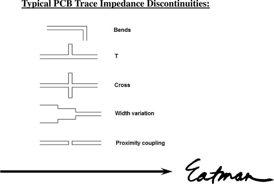
14 Typical PCB Trace Impedance Discontinuities:
15 Propagation Delay: Speed of the signal through a PCB transmission line depends upon the board material Higher dielectric constant (ε r ) = lower speed Propagation delay is important when estimating clock skew on PC boards Formula for signal velocity on a stripline:

16 Types of PC Board Transmission Lines

17 Surface Microstrip: Estimated Z 0 : Signal velocity ~ c/sqrt(0.475 ε r )

18 Surface Microstrip: Advantages: Air dielectric on top - lower combined dielectric constant - higher speed Top conductor can be probed during prototyping Cheaper to implement fewer PC board layers Disadvantages: Radiates EMI off the top of the board Is susceptible to EMI


19 Surface Microstrip Variants: Embedded Microstrip Embedded Microstrip

20 Symmetric Stripline: Estimated Z 0 : Signal velocity ~ c/sqrt(ε r )

21 Stripline: Advantages: Signal traces shielded less EMI, less crosstalk Disadvantages: Difficult to troubleshoot no top board access More costly (more layers) For flex circuits, less flexible (thicker) Slower speed

22 Stripline variants: Edge-coupled Stripline Asymmetric Stripline
 Edge-coupled CPW with")
23 Other Surface Topologies: Coplanar Waveguide (CPW) Edge-coupled CPW with Ground (CPWG)
24 Which One is Best? Lower board cost: Surface topologies (microstrip and CPW use fewer layers) Ease of prototyping: Surface topologies easier to troubleshoot Low loss: CPW Best EMI performance: Stripline Lowest impedance: Stripline Metal shields often used to reduce EMI from surface traces and components
25 Which One is Best? Adhesiveless flex circuit cores have better thickness control Teflon composite flex material can have ε r as low as 2.3 and loss tangent of.0015 Low Dk rigid board laminates are also available - suitable for very high speeds Soldermasks have dielectric properties and loss tangents similar to board materials - affects performance of microstrip and CPW
26 Reducing Unwanted Coupling (Crosstalk)
27 Reducing Unwanted Coupling (Crosstalk): Crosstalk is caused by undesired capacitive, inductive, or conductive coupling from one circuit, part of a circuit, or channel, to another. Coupling affects impedance. A transmission line can be a EMI source and/or victim Reducing unwanted coupling requires reorientation, distance, or shielding Effect of coupling decreases with the square of the distance between the conductors
28 Minimizing Crosstalk: Use striplines or embedded microstrips vs microstrips Minimize congestion of traces through component placement Move signal lines as close to the ground plane as possible - while maintaining the desired impedance Minimize parallel run lengths between signals Route signals on different layers orthogonal to each other
29 Minimizing Crosstalk: For single-ended line: Keep adjacent traces as far apart as possible - at least 2 trace widths For a differential pair: crosstalk cancels out Route differential pair traces (for one signal) as close together as possible Use differential pairs with equal length lines Nested bends = unequal length traces
30 Transmission Line Losses
31 Components of Attenuation / Signal Loss: Metal (resistive) losses - skin effect loss proportional to sqrt (frequency) - also affected by metal surface roughness ( tooth ) Dielectric loss - proportional to frequency see loss tangent Dielectric conductivity loss - stable over frequency - may be ignored if resistivity > 10,000 Ohm-cm Radiation loss
32 Bad Design Bad Performance Choose the right PC board materials: - choose material frequency of use - choose metal for frequency Use good general PC board layout practices: - don t route separate signals in parallel - eliminate sharp corners on traces - avoid ground plane slots - use clean return paths directly under signal lines - pick the right stackup - etc
33 PC Board Manufacturing Issues Affecting Impedance: Interlayer voids = capacitance Pre-preg thickness variation = capacitance Poor via-to-pad registration - drill deflection Inconsistent etching varying trace widths RA copper has less tooth than ED copper Vendor and processes affect your outcome
34 Transmission line design goals: Perfect transfer of power (signal) from one end to the other (source to load) No signal reflections down the line (no discontinuities) No radiated or induced EMI (no coupling or crosstalk) No amplitude reduction (no resistive or dielectric losses) All this in a double sided board with a tight layout, dirt cheap materials, and a sketchy board fabricator NOT EXACTLY
35 The End
Grounding Demystified
 Grounding Demystified 3-1 Importance Of Grounding Techniques 45 40 35 30 25 20 15 10 5 0 Grounding 42% Case 22% Cable 18% Percent Used Filter 12% PCB 6% Grounding 42% Case Shield 22% Cable Shielding 18%
The Critical Length of a Transmission Line
 Page 1 of 9 The Critical Length of a Transmission Line Dr. Eric Bogatin President, Bogatin Enterprises Oct 1, 2004 Abstract A transmission line is always a transmission line. However, if it is physically
PCB Design Conference - East Keynote Address EMC ASPECTS OF FUTURE HIGH SPEED DIGITAL DESIGNS
 OOOO1 PCB Design Conference - East Keynote Address September 12, 2000 EMC ASPECTS OF FUTURE HIGH SPEED DIGITAL DESIGNS By Henry Ott Consultants Livingston, NJ 07039 (973) 992-1793 www.hottconsultants.com
IDT80HSPS1616 PCB Design Application Note - 557
 IDT80HSPS1616 PCB Design Application Note - 557 Introduction This document is intended to assist users to design in IDT80HSPS1616 serial RapidIO switch. IDT80HSPS1616 based on S-RIO 2.0 spec offers 5Gbps
Time and Frequency Domain Analysis for Right Angle Corners on Printed Circuit Board Traces
 Time and Frequency Domain Analysis for Right Angle Corners on Printed Circuit Board Traces Mark I. Montrose Montrose Compliance Services 2353 Mission Glen Dr. Santa Clara, CA 95051-1214 Abstract: For years,
PL-277x Series SuperSpeed USB 3.0 SATA Bridge Controllers PCB Layout Guide
 Application Note PL-277x Series SuperSpeed USB 3.0 SATA Bridge Controllers PCB Layout Guide Introduction This document explains how to design a PCB with Prolific PL-277x SuperSpeed USB 3.0 SATA Bridge
Guidelines for Designing High-Speed FPGA PCBs
 Guidelines for Designing High-Speed FPGA PCBs February 2004, ver. 1.1 Application Note Introduction Over the past five years, the development of true analog CMOS processes has led to the use of high-speed
Comprehensive Analysis of Flexible Circuit Materials Performance in Frequency and Time Domains
 Comprehensive Analysis of Flexible Circuit Materials Performance in Frequency and Time Domains Glenn Oliver and Deepu Nair DuPont Jim Nadolny Samtec, Inc. glenn.e.oliver@dupont.com jim.nadolny@samtec.com
How to make a Quick Turn PCB that modern RF parts will actually fit on!
 How to make a Quick Turn PCB that modern RF parts will actually fit on! By: Steve Hageman www.analoghome.com I like to use those low cost, no frills or Bare Bones [1] type of PCB for prototyping as they
This application note is written for a reader that is familiar with Ethernet hardware design.
 AN18.6 SMSC Ethernet Physical Layer Layout Guidelines 1 Introduction 1.1 Audience 1.2 Overview SMSC Ethernet products are highly-integrated devices designed for 10 or 100 Mbps Ethernet systems. They are
Application Note AN:005. FPA Printed Circuit Board Layout Guidelines. Introduction Contents. The Importance of Board Layout
 FPA Printed Circuit Board Layout Guidelines By Paul Yeaman Principal Product Line Engineer V I Chip Strategic Accounts Introduction Contents Page Introduction 1 The Importance of 1 Board Layout Low DC
RF / Microwave PC Board Design and Layout
 RF / Microwave PC Board Design and Layout Rick Hartley L-3 Avionics Systems richard.hartley@l-3com.com 1 Contents 1) Recommended Reading List 2) Basics 3) Line Types and Impedance 4) Integral Components
Digital Systems Ribbon Cables I CMPE 650. Ribbon Cables A ribbon cable is any cable having multiple conductors bound together in a flat, wide strip.
 Ribbon Cables A ribbon cable is any cable having multiple conductors bound together in a flat, wide strip. Each dielectric configuration has different high-frequency characteristics. All configurations
Application Note: PCB Design By: Wei-Lung Ho
 Application Note: PCB Design By: Wei-Lung Ho Introduction: A printed circuit board (PCB) electrically connects circuit components by routing conductive traces to conductive pads designed for specific components
Designing the NEWCARD Connector Interface to Extend PCI Express Serial Architecture to the PC Card Modular Form Factor
 Designing the NEWCARD Connector Interface to Extend PCI Express Serial Architecture to the PC Card Modular Form Factor Abstract This paper provides information about the NEWCARD connector and board design
Connectivity in a Wireless World. Cables Connectors 2014. A Special Supplement to
 Connectivity in a Wireless World Cables Connectors 204 A Special Supplement to Signal Launch Methods for RF/Microwave PCBs John Coonrod Rogers Corp., Chandler, AZ COAX CABLE MICROSTRIP TRANSMISSION LINE
Using Flex in High-Speed Applications
 feature Figure 1: An automotive flex circuit designed to fit into a tight form factor. Using Flex in High-Speed Applications by Glenn Oliver DuPont Electronics and Communications Copper clad circuits in
Extending Rigid-Flex Printed Circuits to RF Frequencies
 Extending -Flex Printed Circuits to RF Frequencies Robert Larmouth Teledyne Electronic Technologies 110 Lowell Rd., Hudson, NH 03051 (603) 889-6191 Gerald Schaffner Schaffner Consulting 10325 Caminito
Compact Integrated Antennas
 Freescale Semiconductor, Inc. Application Note Document Number: AN2731 Rev. 3, 09/2015 Compact Integrated Antennas Designs and Applications for the MC1321x, MC1322x, MC1323x, and MKW40/30/20 1 Introduction
AVX EMI SOLUTIONS Ron Demcko, Fellow of AVX Corporation Chris Mello, Principal Engineer, AVX Corporation Brian Ward, Business Manager, AVX Corporation
 AVX EMI SOLUTIONS Ron Demcko, Fellow of AVX Corporation Chris Mello, Principal Engineer, AVX Corporation Brian Ward, Business Manager, AVX Corporation Abstract EMC compatibility is becoming a key design
AP24026. Microcontroller. EMC Design Guidelines for Microcontroller Board Layout. Microcontrollers. Application Note, V 3.
 Microcontroller Application Note, V 3.0, April 2005 AP24026 for Microcontroller Board Layout Microcontrollers Never stop thinking. TriCore Revision History: 2005-04 V 3.0 Previous Version: 2001-04 Page
Constructing a precision SWR meter and antenna analyzer. Mike Brink HNF, Design Technologist.
 Constructing a precision SWR meter and antenna analyzer. Mike Brink HNF, Design Technologist. Abstract. I have been asked to put together a detailed article on a SWR meter. In this article I will deal
Nexus Technology Review -- Exhibit A
 Nexus Technology Review -- Exhibit A Background A. Types of DSL Lines DSL comes in many flavors: ADSL, ADSL2, ADSL2+, VDSL and VDSL2. Each DSL variant respectively operates up a higher frequency level.
Using Pre-Emphasis and Equalization with Stratix GX
 Introduction White Paper Using Pre-Emphasis and Equalization with Stratix GX New high speed serial interfaces provide a major benefit to designers looking to provide greater data bandwidth across the backplanes
Balancing the Electrical and Mechanical Requirements of Flexible Circuits. Mark Finstad, Applications Engineering Manager, Minco
 Balancing the Electrical and Mechanical Requirements of Flexible Circuits Mark Finstad, Applications Engineering Manager, Minco Table of Contents Abstract...............................................................................................
" PCB Layout for Switching Regulators "
 1 " PCB Layout for Switching Regulators " 2 Introduction Linear series pass regulator I L V IN V OUT GAIN REF R L Series pass device drops the necessary voltage to maintain V OUT at it s programmed value
Lecture 24. Inductance and Switching Power Supplies (how your solar charger voltage converter works)
") Lecture 24 Inductance and Switching Power Supplies (how your solar charger voltage converter works) Copyright 2014 by Mark Horowitz 1 Roadmap: How Does This Work? 2 Processor Board 3 More Detailed Roadmap
Lecture 24 Inductance and Switching Power Supplies (how your solar charger voltage converter works) Copyright 2014 by Mark Horowitz 1 Roadmap: How Does This Work? 2 Processor Board 3 More Detailed Roadmap
Making Sense of Laminate Dielectric Properties By Michael J. Gay and Richard Pangier Isola Group December 1, 2008
 Making Sense of Laminate Dielectric Properties By Michael J. Gay and Richard Pangier Isola Group December 1, 2008 Abstract System operating speeds continue to increase as a function of the consumer demand
EMI and t Layout Fundamentals for Switched-Mode Circuits
 v sg (t) (t) DT s V pp = n - 1 2 V pp V g n V T s t EE core insulation primary return secondary return Supplementary notes on EMI and t Layout Fundamentals for Switched-Mode Circuits secondary primary
Bending, Forming and Flexing Printed Circuits
 Bending, Forming and Flexing Printed Circuits John Coonrod Rogers Corporation Introduction: In the printed circuit board industry there are generally two main types of circuit boards; there are rigid printed
11. High-Speed Differential Interfaces in Cyclone II Devices
 11. High-Speed Differential Interfaces in Cyclone II Devices CII51011-2.2 Introduction From high-speed backplane applications to high-end switch boxes, low-voltage differential signaling (LVDS) is the
EMC Standards: Standards of good EMC engineering
 Electromagnetic Compatibility (EMC) IEEE Definition Origin, control, and measurement of electromagnetic effects on electronic and biologic systems. IEEE EMC Society Areas of Interest EMC Standards: Standards
A wave lab inside a coaxial cable
 INSTITUTE OF PHYSICS PUBLISHING Eur. J. Phys. 25 (2004) 581 591 EUROPEAN JOURNAL OF PHYSICS PII: S0143-0807(04)76273-X A wave lab inside a coaxial cable JoãoMSerra,MiguelCBrito,JMaiaAlves and A M Vallera
Electronic filters design tutorial -2
 In the first part of this tutorial we explored the bandpass filters designed with lumped elements, namely inductors and capacitors. In this second part we will design filters with distributed components
Measuring Parasitic Capacitance and Inductance Using TDR
 Measuring Parasitic apacitance and Inductance Using TDR Time-domain reflectometry (TDR) is commonly used as a convenient method of determining the characteristic impedance of a transmission line or quantifying
This paper will explain some of the more important factors on how UTP wires work; specifically it will cover the following:
 UTP Technology In the late 1970s, unshielded twisted pair (UTP) cabling originated in the computer industry as a means of transmitting digital data over computer networks. This cable was designed to be
Core Power Delivery Network Analysis of Core and Coreless Substrates in a Multilayer Organic Buildup Package
 Core Power Delivery Network Analysis of Core and Coreless Substrates in a Multilayer Organic Buildup Package Ozgur Misman, Mike DeVita, Nozad Karim, Amkor Technology, AZ, USA 1900 S. Price Rd, Chandler,
An equivalent circuit of a loop antenna.
 3.2.1. Circuit Modeling: Loop Impedance A loop antenna can be represented by a lumped circuit when its dimension is small with respect to a wavelength. In this representation, the circuit parameters (generally
Application Note. PCIEC-85 PCI Express Jumper. High Speed Designs in PCI Express Applications Generation 3-8.0 GT/s
 PCIEC-85 PCI Express Jumper High Speed Designs in PCI Express Applications Generation 3-8.0 GT/s Copyrights and Trademarks Copyright 2015, Inc. COPYRIGHTS, TRADEMARKS, and PATENTS Final Inch is a trademark
2/20/2009 3 Transmission Lines and Waveguides.doc 1/3. and Waveguides. Transmission Line A two conductor structure that can support a TEM wave.
 2/20/2009 3 Transmission Lines and Waveguides.doc 1/3 Chapter 3 Transmission Lines and Waveguides First, some definitions: Transmission Line A two conductor structure that can support a TEM wave. Waveguide
Minimizing crosstalk in a high-speed cable-connector assembly.
 Minimizing crosstalk in a high-speed cable-connector assembly. Evans, B.J. Calvo Giraldo, E. Motos Lopez, T. CERN, 1211 Geneva 23, Switzerland John.Evans@cern.ch Eva.Calvo.Giraldo@cern.ch Tomas.Motos-Lopez@cern.ch
Crosstalk effects of shielded twisted pairs
 This article deals with the modeling and simulation of shielded twisted pairs with CST CABLE STUDIO. The quality of braided shields is investigated with respect to perfect solid shields. Crosstalk effects
Planar Inter Digital Capacitors on Printed Circuit Board
 1 Planar Inter Digital Capacitors on Printed Circuit Board Ajayan K.R., K.J.Vinoy Department of Electrical Communication Engineering Indian Institute of Science, Bangalore, India 561 Email {ajayanr jvinoy}
Introduction to Printed Circuit Board Design For EMC Compliance
 Introduction to Printed Circuit Board Design For EMC Compliance Mark Montrose Principle Consultant Montrose Compliance Services, Inc. + 1 (408) 247-5715 mark@montrosecompliance.com www.montrosecompliance.com
PHY3128 / PHYM203 (Electronics / Instrumentation) Transmission Lines. Repeated n times I L
 Transmission Lines. Repeated n times I L") Transmission Lines Introduction A transmission line guides energy from one place to another. Optical fibres, waveguides, telephone lines and power cables are all electromagnetic transmission lines. are
Transmission Lines Introduction A transmission line guides energy from one place to another. Optical fibres, waveguides, telephone lines and power cables are all electromagnetic transmission lines. are
APPLICATION NOTES POWER DIVIDERS. Things to consider
 Internet Copy Rev A Overview Various RF applications require power to be distributed among various paths. The simplest way this can be done is by using a power splitter/divider. Power dividers are reciprocal
Electromagnetic Compatibility Considerations for Switching Power Supplies
 Electromagnetic Compatibility Considerations Characterization of the EMI problem requires understanding the interference source Switching power supplies generate Electromagnetic Interference (EMI) by virtue
Application Note 58 Crystal Considerations with Dallas Real Time Clocks
 www.dalsemi.com Application Note 58 Crystal Considerations with Dallas Real Time Clocks Dallas Semiconductor offers a variety of real time clocks (RTCs). The majority of these are available either as integrated
Impedance Matching and Matching Networks. Valentin Todorow, December, 2009
 Impedance Matching and Matching Networks Valentin Todorow, December, 2009 RF for Plasma Processing - Definition of RF What is RF? The IEEE Standard Dictionary of Electrical and Electronics Terms defines
SECTION 2 Transmission Line Theory
 SEMICONDUCTOR DESIGN GUIDE Transmission Line Theory SECTION 2 Transmission Line Theory Introduction The ECLinPS family has pushed the world of ECL into the realm of picoseconds. When output transitions
A SURVEY AND TUTORIAL OF DIELECTRIC MATERIALS USED IN THE MANUFACTURE OF PRINTED CIRCUIT BOARDS.
 A SURVEY AND TUTORIAL OF DIELECTRIC MATERIALS USED IN THE MANUFACTURE OF PRINTED CIRCUIT BOARDS. By Lee W. Ritchey, Speeding Edge, for publication in November 1999 issue of Circuitree magazine. Copyright
RF / Microwave PC Board Design and Layout Base Materials for High Speed, High Frequency PC Boards Rick Hartley
 RF / Microwave PC Board Design and Layout Base Materials for High Speed, High Frequency PC Boards Rick Hartley http://www.qsl.net/va3iul/ RF / Microwave Design Basics Unlike digital, analog signals can
Connector Launch Design Guide
 WILD RIVER TECHNOLOGY LLC Connector Launch Design Guide For Vertical Mount RF Connectors James Bell, Director of Engineering 4/23/2014 This guide will information on a typical launch design procedure,
How To Design An Ism Band Antenna For 915Mhz/2.4Ghz Ism Bands On A Pbbb (Bcm) Board
 Board") APPLICATION NOTE Features AT09567: ISM Band PCB Antenna Reference Design Atmel Wireless Compact PCB antennas for 915MHz and 2.4GHz ISM bands Easy to integrate Altium design files and gerber files Return
APPLICATION NOTE Features AT09567: ISM Band PCB Antenna Reference Design Atmel Wireless Compact PCB antennas for 915MHz and 2.4GHz ISM bands Easy to integrate Altium design files and gerber files Return
ATE-A1 Testing Without Relays - Using Inductors to Compensate for Parasitic Capacitance
 Introduction (Why Get Rid of Relays?) Due to their size, cost and relatively slow (millisecond) operating speeds, minimizing the number of mechanical relays is a significant goal of any ATE design. This
IIB. Complete PCB Design Using OrCAD Capture and PCB Editor. Kraig Mitzner. ~»* ' AMSTERDAM BOSTON HEIDELBERG LONDON ^ i H
 Complete PCB Design Using OrCAD Capture and PCB Editor Kraig Mitzner IIB ~»* ' AMSTERDAM BOSTON HEIDELBERG LONDON ^ i H NEW YORK * OXFORD PARIS SAN DIEGO ШШЯтИ' ELSEVIER SAN FRANCISCO SINGAPORE SYDNEY
ILB, ILBB Ferrite Beads
 ILB, ILBB Ferrite Beads Electro-Magnetic Interference and Electro-Magnetic Compatibility (EMI/EMC) avid B. Fancher Inductive Products ivision INTROUCTION Manufacturers of electrical and electronic equipment
Optimised For Audio Analogue PCB design for the digital era.
 Optimised For Audio Analogue PCB design for the digital era. David G. Tyas IKON AVS Ltd, 238 Ikon Estate, Hartlebury, Worcs.. DY10 4EU www.ikonavs.com 1. Introduction With increasing emphasis on digital
Return Paths and Power Supply Decoupling
 Return Paths and Power Supply Decoupling Dr. José Ernesto Rayas Sánchez 1 Outline Ideal return paths Microstrip return paths Stripline return paths Modeling metallic reference planes Power supply bypassing
X2Y Solution for Decoupling Printed Circuit Boards
 Summary As printed circuit board s (PCB) power distribution systems (PDS) gain in complexity (i.e. multiple voltages and lower voltages levels) the sensitivity to transients and noise voltage is becoming
Signal Integrity: Tips and Tricks
 White Paper: Virtex-II, Virtex-4, Virtex-5, and Spartan-3 FPGAs R WP323 (v1.0) March 28, 2008 Signal Integrity: Tips and Tricks By: Austin Lesea Signal integrity (SI) engineering has become a necessary
Radiated Emission and Susceptibility
 Radiated Emission and Susceptibility Tzong-Lin Wu, Ph.D. EMC Lab Department of Electrical Engineering National Taiwan University Differential-Mode v.s. Common-mode Currents 1 Differential-Mode v.s. Common-mode
Utilizing Time Domain (TDR) Test Methods For Maximizing Microwave Board Performance
 Test Methods For Maximizing Microwave Board Performance") The Performance Leader in Microwave Connectors Utilizing Time Domain (TDR) Test Methods For Maximizing Microwave Board Performance.050 *.040 c S11 Re REF 0.0 Units 10.0 m units/.030.020.010 1.0 -.010 -.020
The Performance Leader in Microwave Connectors Utilizing Time Domain (TDR) Test Methods For Maximizing Microwave Board Performance.050 *.040 c S11 Re REF 0.0 Units 10.0 m units/.030.020.010 1.0 -.010 -.020
Modeling Physical Interconnects (Part 3)
") Modeling Physical Interconnects (Part 3) Dr. José Ernesto Rayas Sánchez 1 Outline Vias Vias in PCBs Types of vias in PCBs Pad and antipad Nonfunctional pads Modeling vias Calculating circuit element values
Modeling Physical Interconnects (Part 3) Dr. José Ernesto Rayas Sánchez 1 Outline Vias Vias in PCBs Types of vias in PCBs Pad and antipad Nonfunctional pads Modeling vias Calculating circuit element values
EM Noise Mitigation in Circuit Boards and Cavities
 EM Noise Mitigation in Circuit Boards and Cavities Faculty (UMD): Omar M. Ramahi, Neil Goldsman and John Rodgers Visiting Professors (Finland): Fad Seydou Graduate Students (UMD): Xin Wu, Lin Li, Baharak
UNDERSTANDING AND CONTROLLING COMMON-MODE EMISSIONS IN HIGH-POWER ELECTRONICS
 Page 1 UNDERSTANDING AND CONTROLLING COMMON-MODE EMISSIONS IN HIGH-POWER ELECTRONICS By Henry Ott Consultants Livingston, NJ 07039 (973) 992-1793 www.hottconsultants.com hott@ieee.org Page 2 THE BASIC
Video Camera Installation Guide
 Video Camera Installation Guide The intent of this guide is to provide the information needed to complete or modify a video camera installation to avoid lightning and induced power surge damage. This guide
Simulation and Design Route Development for ADEPT-SiP
 Simulation and Design Route Development for ADEPT-SiP Alaa Abunjaileh, Peng Wong and Ian Hunter The Institute of Microwaves and Photonics School of Electronic and Electrical Engineering The University
Common Mode Choke Filtering Improves CMRR in Ethernet Transformer Applications. Application Note. June 2011
 Common Mode Choke Filtering Improves CMRR in Ethernet Transformer Applications June 2011 Application Note Common mode chokes provide an effective EMI filtering solution for Ethernet transformer applications.
Coaxial Cable Products Guide. Connectivity for Business-Critical Continuity
 Coaxial Cable Products Guide Connectivity for Business-Critical Continuity The Difference Starts With The Cable BULK CABLES SLA Series Lowest loss cable available to 18 GHz, best choice for critical applications
Capacitor Self-Resonance
 Capacitor Self-Resonance By: Dr. Mike Blewett University of Surrey United Kingdom Objective This Experiment will demonstrate some of the limitations of capacitors when used in Radio Frequency circuits.
Precision Analog Designs Demand Good PCB Layouts. John Wu
 Precision Analog Designs Demand Good PCB Layouts John Wu Outline Enemies of Precision: Hidden components Noise Crosstalk Analog-to-Analog Digital-to-Analog EMI/RFI Poor Grounds Thermal Instability Leakage
Standex-Meder Electronics. Custom Engineered Solutions for Tomorrow
 Standex-Meder Electronics Custom Engineered Solutions for Tomorrow RF Reed Relays Part II Product Training Copyright 2013 Standex-Meder Electronics. All rights reserved. Introduction Purpose Designing
2. A conductor of length 2m moves at 4m/s at 30 to a uniform magnetic field of 0.1T. Which one of the following gives the e.m.f. generated?
 Extra Questions - 2 1. A straight length of wire moves through a uniform magnetic field. The e.m.f. produced across the ends of the wire will be maximum if it moves: a) along the lines of magnetic flux
Current and Temperature Ratings
 Document 361-1 Current and Temperature Ratings Introduction This application note describes: How to interpret Coilcraft inductor current and temperature ratings Our current ratings measurement method and
DRAFT. University of Pennsylvania Moore School of Electrical Engineering ESE319 Electronic Circuits - Modeling and Measurement Techniques
 University of Pennsylvania Moore School of Electrical Engineering ESE319 Electronic Circuits - Modeling and Measurement Techniques 1. Introduction. Students are often frustrated in their attempts to execute
EDEXCEL NATIONAL CERTIFICATE/DIPLOMA UNIT 5 - ELECTRICAL AND ELECTRONIC PRINCIPLES NQF LEVEL 3 OUTCOME 4 - ALTERNATING CURRENT
 EDEXCEL NATIONAL CERTIFICATE/DIPLOMA UNIT 5 - ELECTRICAL AND ELECTRONIC PRINCIPLES NQF LEVEL 3 OUTCOME 4 - ALTERNATING CURRENT 4 Understand single-phase alternating current (ac) theory Single phase AC
T = 1 f. Phase. Measure of relative position in time within a single period of a signal For a periodic signal f(t), phase is fractional part t p
, phase is fractional part t p") Data Transmission Concepts and terminology Transmission terminology Transmission from transmitter to receiver goes over some transmission medium using electromagnetic waves Guided media. Waves are guided
Data Transmission Concepts and terminology Transmission terminology Transmission from transmitter to receiver goes over some transmission medium using electromagnetic waves Guided media. Waves are guided
The Evolution of Copper Cabling Systems from Cat5 to Cat5e to Cat6 Copper Cabling Standards and Technical Aspects
 The Evolution of Copper Cabling Systems from Cat5 to Cat5e to Cat6 Copper Cabling Standards and Technical Aspects White Paper /7/0 Executive Summary Now that the TIA/EIA-568-B.- Category 6 Copper Cabling
WHITEPAPER. Cable and Connector for Hiperface dsl motor drive applications
 WHITEPAPER Cable and Connector for Hiperface dsl motor drive applications information for cable manufacturers Version 02 Content Information for cable manufacturers...3 Communication...3 Crosstalk & shielding...3
GenTech Practice Questions
 GenTech Practice Questions Basic Electronics Test: This test will assess your knowledge of and ability to apply the principles of Basic Electronics. This test is comprised of 90 questions in the following
Switching Regulator Series PCB Layout Techniques of Buck Converter
 Switching Regulator Series PCB ayout Techniques of Buck Converter No.07EBY05 PCB layout design for switching power supply is as important as the circuit design. Appropriate layout can avoid various problems
Broadband Slotted Coaxial Broadcast Antenna Technology
 Broadband Slotted Coaxial Broadcast Antenna Technology Summary Slotted coaxial antennas have many advantages over traditional broadband panel antennas including much smaller size and wind load, higher
Mode Patterns of Parallel plates &Rectangular wave guides Mr.K.Chandrashekhar, Dr.Girish V Attimarad
 International Journal of Scientific & Engineering Research Volume 3, Issue 8, August-2012 1 Mode Patterns of Parallel plates &Rectangular wave guides Mr.K.Chandrashekhar, Dr.Girish V Attimarad Abstract-Parallel
The Importance of the X/R Ratio in Low-Voltage Short Circuit Studies
 The Importance of the X/R Ratio in Low-Voltage Short Circuit Studies DATE: November 17, 1999 REVISION: AUTHOR: John Merrell Introduction In some short circuit studies, the X/R ratio is ignored when comparing
S-PARAMETER MEASUREMENTS OF MEMS SWITCHES
 Radant MEMS employs adaptations of the JMicroTechnology test fixture depicted in Figure 1 to measure MEMS switch s-parameters. RF probeable JMicroTechnology microstrip-to-coplanar waveguide adapter substrates
SICK AG WHITEPAPER. Information for cable manufacturers Note-2_03
 SICK AG WHITEPAPER Cable and connector for HIPERFACE DSL motor drive applications Information for cable manufacturers Note-2_03 Juergen Funkhaenel Application Engineer at SICK STEGMANN GmbH Donaueschingen
Experiment 7: Familiarization with the Network Analyzer
 Experiment 7: Familiarization with the Network Analyzer Measurements to characterize networks at high frequencies (RF and microwave frequencies) are usually done in terms of scattering parameters (S parameters).
Application Note 58 Crystal Considerations for Dallas Real-Time Clocks
 www.maxim-ic.com Application Note 58 Crystal Considerations for Dallas Real-Time Clocks OVERVIEW This application note describes crystal selection and layout techniques for connecting a 32,768Hz crystal
Interfacing Intel 8255x Fast Ethernet Controllers without Magnetics. Application Note (AP-438)
") Interfacing Intel 8255x Fast Ethernet Controllers without Magnetics Application Note (AP-438) Revision 1.0 November 2005 Revision History Revision Revision Date Description 1.1 Nov 2005 Initial Release
Interfacing Intel 8255x Fast Ethernet Controllers without Magnetics Application Note (AP-438) Revision 1.0 November 2005 Revision History Revision Revision Date Description 1.1 Nov 2005 Initial Release
Signal Types and Terminations
 Helping Customers Innovate, Improve & Grow Application Note Signal Types and Terminations Introduction., H, LV, Sinewave, Clipped Sinewave, TTL, PECL,,, CML Oscillators and frequency control devices come
WAVEGUIDE-COAXIAL LINE TRANSITIONS
 WAVEGUIDE-COAXIAL LINE TRANSITIONS 1. Overview Equipment at microwave frequencies is usually based on a combination of PCB and waveguide components. Filters and antennas often use waveguide techniques,
National Laboratory of Antennas and Microwave Technology Xidian University Xi an, Shaanxi 710071, China
 Progress In Electromagnetics Research, PIER 76, 237 242, 2007 A BROADBAND CPW-FED T-SHAPE SLOT ANTENNA J.-J. Jiao, G. Zhao, F.-S. Zhang, H.-W. Yuan, and Y.-C. Jiao National Laboratory of Antennas and Microwave
Oscar E. Morel UtilX Corporation
 Oscar E. Morel UtilX Corporation Time Domain Reflectometry (TDR) has been the preferred technique to assess: Cable length Splice number and spatial location, and Metallic neutral condition Tests for neutral
The Don ts of Better Flexible Circuit Design and Manufacture By Mark Finstad Friday, 01 June 2007
 The Don ts of Better Flexible Circuit Design and Manufacture By Mark Finstad Friday, 01 June 2007 Successful designs are soon forgotten but failures are remembered for years. Steering clear of these twelve
What Really Is Inductance?
 Bogatin Enterprises, Dr. Eric Bogatin 26235 W 110 th Terr. Olathe, KS 66061 Voice: 913-393-1305 Fax: 913-393-1306 eric@bogent.com www.bogatinenterprises.com Training for Signal Integrity and Interconnect
Transmission Lines in Communication Systems FACET
 Computer-Based Electronics Training System Transmission Lines in Communication Systems FACET 36970- Order no.: 36970-00 First Edition Revision level: 02/2015 By the staff of Festo Didactic Festo Didactic
DEPARTMENT OF DEFENSE TEST METHOD STANDARD METHOD OF INSERTION LOSS MEASUREMENT
 INCH-POUND MIL-STD-220C 14 May 2009 SUPERSEDING MIL-STD-220B 24 January 2000 DEPARTMENT OF DEFENSE TEST METHOD STANDARD METHOD OF INSERTION LOSS MEASUREMENT AMSC N/A FSC EMCS FOREWORD 1. This standard
Shielding Effectiveness Test Method. Harbour s LL, SB, and SS Coaxial Cables. Designs for Improved Shielding Effectiveness
 Shielding Effectiveness Test Method Harbour s LL, SB, and SS Coaxial Cables Designs for Improved Shielding Effectiveness Harbour Industries 4744 Shelburne Road Shelburne Vermont 05482 USA 802-985-3311
Current Probes, More Useful Than You Think
 Current Probes, More Useful Than You Think Training and design help in most areas of Electrical Engineering Copyright 1998 Institute of Electrical and Electronics Engineers. Reprinted from the IEEE 1998