High. Thickness. epitaxial Silicon. Carbide Detectors. INFN - Gruppo V 2009
|
|
|
- Magdalen Dixon
- 8 years ago
- Views:
Transcription
1 INFN - Gruppo V Proposta di nuovo esperimento per il triennio High Thickness epitaxial Silicon Carbide Detectors Sezioni INFN di Milano - Bologna - Catania

2 Outline A general introduction on Silicon Carbide SiC detectors: International R&D INFN Research Activity on SiC Radiation Detectors HiTSiC Proposal

3 A General Introduction on Silicon Carbide

4 SiC politypes 3C-SiC (E G = 2.2 ev) 4H-SiC (E G = 3.3 ev) 6H-SiC (E G = 3 ev)
 6H-SiC (E G")
5 Wide Bandgap E G =3.2 ev Room & High temperature operation SiC properties x 10 x 2.5 x 2 Si GaAs 4H-SiC High saturation velocity v S = 200 µm/ns High frequency/speed devices 0 E g (ev) E c (MV/cm) λ th (W/cmK) V s (10 7 cm/s) High Critical Field E C = 2 MV/cm High Voltage devices High thermal conductivity High Power devices
 E c (MV/cm) λ th (W/cmK) V s (10 7 cm/s) High Critical Field E C")


6 High Performance SiC Electron Devices...a reality

7 SiC High Performance Electron Devices The highest V B diode Kansai corp. Power MOSFET: 5 kv - 88 mω cm 2 Reverse Voltage [kv] V B = 19 kv Current [ na ] Rockwell International High Power X-Band MESFET f T f=14.5 T GHz, GHz, f MAX f =38 MAX =38 GHz GHz I Dmax I = Dmax ma, ma, V DSmax =150V DSmax =150V Gain: Gain: db 2 GHz GHz

8 Silicon Carbide Technology a continuous progress

9 Power Device Performance SiC vs. Si 4H-SiC MOSFET 5 kv - 88 mω cm 2 Kansay Co (Japan)- CREE Inc. (USA) 4H-SiC BJT 1.8 kv - 11 mω cm 2 CREE Inc. (USA) 4H-SiC JFET 600 V - 5 mω cm 2 Rockwell (USA)

10 April 2001: first commercial SiC Diode

11 2006: SiC Ultrafast Power Schottky Diodes

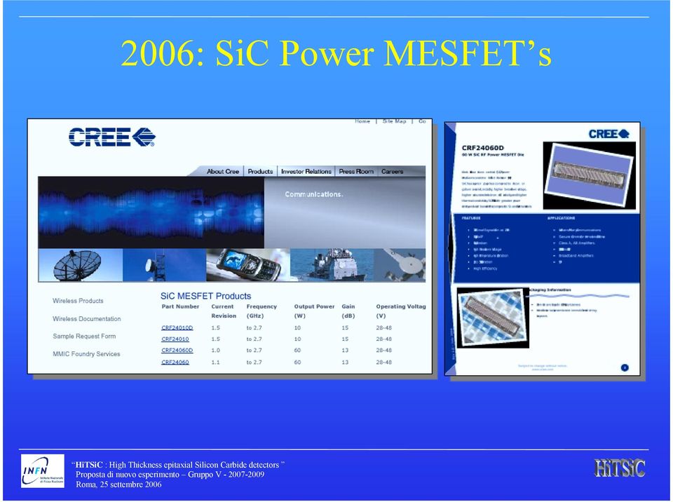
12 2006: SiC Power MESFET s
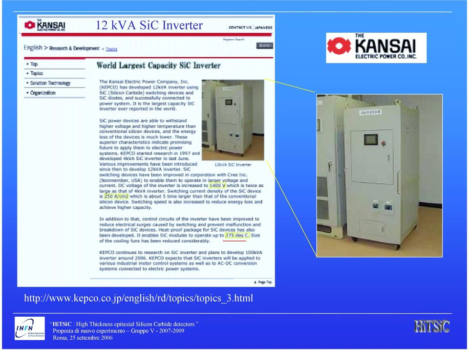
13 12 kva SiC Inverter

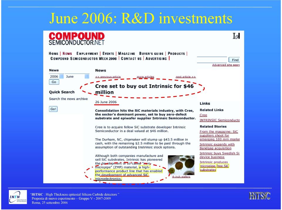
14 June 2006: R&D investments
15 Conclusions on SiC status SiC knowledge and technology is continuously growing Industrial R&D are running SiC power device gives better performance than Si counterpart High performance SiC diodes & MESFET s on market Material quality is continuously improving

16 Silicon Carbide Radiation Detectors Motivation International R&D INFN R&D

17 Wide Bandgap High Schottky / pn barriers Low thermally generated currents No cooling required High temperature Silicon Carbide Properties benefits for radiation detectors ev 2 MV/cm 3.8 W/cmK Si GaAs 4H-SiC 200 µm/ns 1 0 High Critical Field High Bias Voltage Reduced Soft Breakdown No guard rings necessity E g (ev) E c (MV/cm) High thermal conductivity Easy T control FEE cooling λ th (W/cmK) V s (10 7 cm/s) High saturation velocity short transit time Fast signals Low trapping probability
 E c (MV/cm) High thermal conductivity Easy T control FEE cooling λ th (W/cmK) V s (10 7 cm/s) High saturation velocity")


18 SiC Detectors European Research Activity

19 Westinghouse SiC Detectors CREE Inc. Reactor core SiC detector Dulloo, Ruddy et al., IEEE Trans. Nucl. Science 46, 1999

20 Naval Research Laboratory Brookhaven National Laboratory CREE Inc.

21 INFN Research Activity on SiC Radiation Detectors
22 INFN SiCPOS experiment ( ) Pad detectors Microstrips SiC wafers: Pixel detectors SiC Technology:
23 Results: Detector Leakage Current Density Schottky contact - Au n - epilayer 5x µm n+ buffer 1 µm n+ substrate µm ohmic contact - Ti/Pt/Au Current density [ A / cm 2 ] Room Temperature CdTe CdZnTe Silicon 1000 SI LEC GaAs (pn) VPE GaAs (SJ) +127 C SiC Mean electric field [ kv / cm ] 10-5 Si / GaAs 1 na/cm SiC 1 pa/cm 2
24 SiC Pixels Detectors Performance RT Leakage Current vs. Bias Pixel Reverse Current 10 fa 1 fa ENC PW 300 K 27 C 400 x 400 µm 2 PIXEL 200 x 200 µm 2 PIXEL Reverse Voltage [ V ] < 10 fa < 1 fa The Front-End Issue! 0.1 fa The Front-End Issue! 1 [ fa] τ [ s] [ e r. m..] = I peak µ s Number of pixels ± 0.1 e ± 0.1 e Pixel Noise [ electrons r.m.s. ] + 27 C II fa fa ENC ENC (τ=20µs) < 1 ee - - rms rms Sub-Electron Noise Detectors (Fano (Fano limited) limited) G. Bertuccio, S. Caccia, R. Casiraghi, C. Lanzieri IEEE Trans. Nucl. Sci., 53 n.4, August 2006, pp
25 Ultra Low Noise CMOS Charge Amplifier for SiC Detectors S ID [ A 2 Hz -1 ] CMOS Preamplifier chip 1 / f k 10k f [Hz] 100k 1M LF Noise modelling 300µA 100µA 30µA 10µA G. Bertuccio and S. Caccia, E N C [ e- r.m.s. ] e e - r.m.s. - r.m.s Shaping Time [ µs ] Measured ENC e e - r.m.s. - r.m.s. Invited talk at the 11 th Symposium on Radiation Measurements and Applications, Ann Arbor, Michigan, USA, May 23-25, 2006 Submitted to NIM A, May 2006 ENC [ electrons r.m.s. ] τ = 12 µs 7.6 e e - - // µw µw ee - - // mw mw 30µW 100µW 1mW 10mW Preamplifier Power Consumption
26 Low- Noise Charge Preamplifiers A New state of the Art ENC [e- r.m.s.] Power [ mw/ch ] Technology Reference CMOS 0.35 µm This work CMOS 0.35 µm This work 9 11 CMOS 1.2 µm BNL [1] 14 8 CMOS 0.35µm BNL [2] 15 6 CMOS 0.5 µm LBL [3] CMOS 0.5 µm Nova [4] 29 - CMOS 1.2 µm Caltech [5]
27 How our Research Activity and Results are seen worldwide? Invited Talks at International Conferences G. Bertuccio " Front-end Amplifiers and ASIC s in Sub-micron CMOS and BiCMOS Technologies for Charge Measurements" Nuclear Science Sympsium and Medical Imaging Conference, October 2003, Portland, USA. G. Bertuccio, R. Casiraghi, F. Nava, M. Bruzzi "Performance of Silicon Carbide Radiation Detectors " 13th International Workshop on Room Temperature Semiconductor Detectors and Associated Electronics, October 2003, Portland, USA. G. Bertuccio "Prospects for Energy Resolving X-ray imaging with Compound Semiconductor Pixel Detectors" 6th International Workshop on Radiation Imaging Detectors, July 2004, Glasgow, Scotland. G. Bertuccio et al. "Silicon Carbide for Alpha, Beta, Ion and soft X-ray High Performance Detectors" 5th European Conference on Silicon Carbide and Related Materials, 31 August-4 September 2004, Bologna, Italy. G. Bertuccio, S. Caccia "Challenges in the Readout Electronics for Room Temperature Semiconductor Radiation Detectors " 14th International Workshop on Room Temperature Semiconductor Detectors and Associated Electronics, October 2004, Rome, Italy. G. Bertuccio, S. Caccia Ultra Low Noise Front-End and ASIC for X-ray Spectroscopy" 11th Symposium on Radiation Detection and Applications, May 2006, Ann Arbor, USA.
28 Present Limit of SiC detectors Schottky contact - Au Depth of depletion layer X D X D n - epilayer 5x µm X D V N R d reverse bias dopant concentration n+ buffer 1 µm n+ substrate µm ohmic contact - Ti/Pt/Au Thick depletion layer N d =5x 10 14, V R =300 V X D = 25 µm ( X D = 70 µm V R = 2.3 kv ) High detection efficiency ( X-rays) High peak/valley ratio (X-rays) Higher signal ( α, e - ) Thick X D requires Low capacitance lower ENC, τ opt Thick Thick // High High purity purity // Defect Defect free free epitaxial layers layers (>100 (>100 µm) µm) Low Low residual residual doping doping N d ( d ( < cm cm -3-3 ))
29 Challenges and open issues for SiC detectors R&D Increase the epitaxial layer thickness Is it possible to grow µm? How to increase the process growth rate? How the crystal defectivity depends on the growth rate? Decrease the residual doping What is the origin of the residual doping? Where does the dopants come from? Is it possible to reach cm -3 with the available reactors / processes or new reactor/process must be introduced? Physics of thick-high purity SiC epitaxial detectors How large will be the leakage current (noise!) in thick SiC detectors? What the values of the electron/hole mean drift length at electric fields E<10kV/cm? What will be the radiation resistance of thick SiC detectors?
30 INFN - Gruppo V Proposta di nuovo esperimento per il triennio High Thickness epitaxial Silicon Carbide Detectors Research group Collaborations Research Activity & Milestones
31 Research Team G. Bertuccio (RN), S. Caccia, E. Gatti, S. Riboldi, S. Masci, M. Sampietro INFN - Milano and Politecnico di Milano (Giuseppe.Bertuccio@polimi.it) F. Nava, M. Bagni, T. Corazzari, P. Errani INFN Bologna and University of Modena (nava.filippo@unimo.it) G. Foti, D. Puglisi INFN and University of Catania (Gaetano.Foti@ct.infn.it) Industrial & other collaborations
32 HiTSiC: overcoming SiC R&D limits Limits of previous SiC detectors R&D Wafer supplier: CREE Inc. (USA) Not the best SiC wafers available Not possibility to change epi-growth specification Epitaxy from IKZ (Germany): low epi-specification control Overcoming limits by means of National wafer supplier: LPE-ETC R&D on SiC epitaxial growth at LPE-ETC Strong feedback with LPE-ETC

33 LPE-ETC: R&D Industrial collaboration

34 LPE-ETC: Epitaxial Reactors & Processes
35 LPE-ETC collaboration Growth rate (µm/hr) T dep =1650 C C/Si=1.0 HCl 40 T dep =1550 C 20 No HCl C/Si=1.5 Silicon precipitates Si/H 2 %


36 SELEX: R&D Industrial collaboration
37 A Complete SiC Detectors R&D in Italy Strong Points Availability of the highest material quality High Thickness Epitaxial Layers ( µm) Lowest residual doping (10 13 cm -3 ) Device to Material Feedback Material Wafer Production Characterisation Detector/FEE design & fabrication Detector/FEE characterisation Current [ A ] 10-6 t=127 C t=47 C t=24 C t=67 C t=107 C t=87 C Forward Voltage [ V ] kev 241 Am Counts kev RMS (nm) HCl process STD process 5 x 5 µm Energy [ kev ] INFN Milano & Bologna Growth rate (µm/h) INFN Catania & IMM Feedback
38 HiTSiC Research Activity INFN INFN Milano Milano INFN INFN Catania Catania TASKS INFN INFN Bologna Bologna DETECTOR DESIGN DETECTOR DESIGN FRONT END ELECRONICS DESIGN FRONT END ELECRONICS DESIGN DETECTOR ELECTRICAL CHAR. DETECTOR ELECTRICAL CHAR. X-RAY SPECTROSCOPIC CHAR. X-RAY SPECTROSCOPIC CHAR. SiC GROWTH SiC GROWTH SiC MATERIAL SiC MATERIAL CHARACTERIZATION CHARACTERIZATION (DLTS RBS-Channeling, Low (DLTS RBS-Channeling, Low Temperature PL) Temperature PL) JUNCTION DEVELOPMENT. JUNCTION DEVELOPMENT. DETECTOR CHARACTERIZATION DETECTOR (α, β). CHARACTERIZATION (α, β). RADIATION RESISTANCE RADIATION RESISTANCE MILESTONES TECHNOLOGICAL: - Growth of SiC wafers with High Thickness / High Purity / Low defect density - Ultra Thin Ultra Low leakage Schottky Junction - High Yield Large Area Detector Fabrication SCIENTIFIC & APPLIED: - High Resolution Wide Temperature Detectors - SiC Crystal knowledge (imputities/deep&shallow levels/traps/defects) - Custom Ultra-low Noise Front-End Electronics
Silicon Drift Detector Product Brochure Update 2013
 Silicon Drift Detector Product Brochure Update 2013 Content Classic Silicon Drift Detector High Resolution Silicon Drift Detector Multielement Silicon Detector Extra Large Detector Series July 2013 About
Solid State Detectors = Semi-Conductor based Detectors
 Solid State Detectors = Semi-Conductor based Detectors Materials and their properties Energy bands and electronic structure Charge transport and conductivity Boundaries: the p-n junction Charge collection
Characteristics of blocking voltage for power 4H-SiC BJTs with mesa edge termination
 Vol. 31, No. 7 Journal of Semiconductors July 2010 Characteristics of blocking voltage for power 4H-SiC BJTs with mesa edge termination Zhang Qian( 张 倩 ), Zhang Yuming( 张 玉 明 ), and Zhang Yimen( 张 义 门
organismos internacionales
 Semiconductores de potencia de gap ancho en organismos internacionales Philippe Godignon & Power devices and Systems Group Systems Integration Department Centro Nacional de Microelectrónica, CNM CNM-CSIC,
SiC activities at Linköping University
 SiC activities at Linköping University A. Henry and E. Janzén SiC : Prof. Erik Janzen growth (bulk and epi) defect and characterisation Nitride : Prof. Bo Monemar growth optical characterisation Electronic
(Amplifying) Photo Detectors: Avalanche Photodiodes Silicon Photomultiplier
 Photo Detectors: Avalanche Photodiodes Silicon Photomultiplier") (Amplifying) Photo Detectors: Avalanche Photodiodes Silicon Photomultiplier (no PiN and pinned Diodes) Peter Fischer P. Fischer, ziti, Uni Heidelberg, Seite 1 Overview Reminder: Classical Photomultiplier
(Amplifying) Photo Detectors: Avalanche Photodiodes Silicon Photomultiplier (no PiN and pinned Diodes) Peter Fischer P. Fischer, ziti, Uni Heidelberg, Seite 1 Overview Reminder: Classical Photomultiplier
CONTENTS. Preface. 1.1.2. Energy bands of a crystal (intuitive approach)
") CONTENTS Preface. Energy Band Theory.. Electron in a crystal... Two examples of electron behavior... Free electron...2. The particle-in-a-box approach..2. Energy bands of a crystal (intuitive approach)..3.
CONTENTS Preface. Energy Band Theory.. Electron in a crystal... Two examples of electron behavior... Free electron...2. The particle-in-a-box approach..2. Energy bands of a crystal (intuitive approach)..3.
Indirect X-ray photon counting image sensor with 27T pixels and 15 electrons RMS accurate threshold
 Indirect X-ray photon counting image sensor with 27T pixels and 15 electrons RMS accurate threshold B. Dierickx 1,2, B. Dupont 1,3, A. Defernez 1, N. Ahmed 1 1 Caeleste, Antwerp, Belgium 2 Vrije Universiteit
Silicon Sensors for CMS Tracker at High-Luminosity Environment - Challenges in particle detection -
 timo.peltola@helsinki.fi Finnish Society for Natural Philosophy, Helsinki, 17 February 2015 Silicon Sensors for CMS Tracker at High-Luminosity Environment - Challenges in particle detection - Timo Peltola
BPW34. Silicon PIN Photodiode VISHAY. Vishay Semiconductors
 Silicon PIN Photodiode Description The is a high speed and high sensitive PIN photodiode in a miniature flat plastic package. Its top view construction makes it ideal as a low cost replacement of TO-5
Nuclear Weapons and Material Security (WMS) Team Program Review WMS2013
 Team Program Review WMS2013") Office of Research & Development Nuclear Weapons and Material Security (WMS) Team Program Review WMS2013 Array of Virtual Frisch-Grid CZT Detectors with Common Cathode Readout for Correcting Charge Trapping
Office of Research & Development Nuclear Weapons and Material Security (WMS) Team Program Review WMS2013 Array of Virtual Frisch-Grid CZT Detectors with Common Cathode Readout for Correcting Charge Trapping
Chip Diode Application Note
 Chip Diode Application Note Introduction The markets of portable communications, computing and video equipment are challenging the semiconductor industry to develop increasingly smaller electronic components.
Technology Developments Towars Silicon Photonics Integration
 Technology Developments Towars Silicon Photonics Integration Marco Romagnoli Advanced Technologies for Integrated Photonics, CNIT Venezia - November 23 th, 2012 Medium short reach interconnection Example:
Bob York. Transistor Basics - MOSFETs
 Bob York Transistor Basics - MOSFETs Transistors, Conceptually So far we have considered two-terminal devices that are described by a current-voltage relationship I=f(V Resistors: Capacitors: Inductors:
Gamma and X-Ray Detection
 Gamma and X-Ray Detection DETECTOR OVERVIEW The kinds of detectors commonly used can be categorized as: a. Gas-filled Detectors b. Scintillation Detectors c. Semiconductor Detectors The choice of a particular
Advantages of SiC MOSFETs in Power Applications
 Advantages of SiC MOSFETs in Power Applications Power Forum, Bologna September 18 th, 2014 Pascal Ducluzeau Product Marketing Director Microsemi Power Module Products pducluzeau@microsemi.com Topics Advantages
PIN CONFIGURATION FEATURES ORDERING INFORMATION ABSOLUTE MAXIMUM RATINGS. D, F, N Packages
 DESCRIPTION The µa71 is a high performance operational amplifier with high open-loop gain, internal compensation, high common mode range and exceptional temperature stability. The µa71 is short-circuit-protected
Lecture 030 DSM CMOS Technology (3/24/10) Page 030-1
 Page 030-1") Lecture 030 DSM CMOS Technology (3/24/10) Page 030-1 LECTURE 030 - DEEP SUBMICRON (DSM) CMOS TECHNOLOGY LECTURE ORGANIZATION Outline Characteristics of a deep submicron CMOS technology Typical deep submicron
Lecture 030 DSM CMOS Technology (3/24/10) Page 030-1 LECTURE 030 - DEEP SUBMICRON (DSM) CMOS TECHNOLOGY LECTURE ORGANIZATION Outline Characteristics of a deep submicron CMOS technology Typical deep submicron
ISTITUTO NAZIONALE DI FISICA NUCLEARE
 ISTITUTO NAZIONALE DI FISICA NUCLEARE Sezione di Trieste INFN/TC-2/7 1 aprile 22 A novel scheme for the integrated voltage divider of Silicon Drift Detectors P. Burger 1, C. Piemonte 2, A. Rashevsky 3,
Application Note 58 Crystal Considerations with Dallas Real Time Clocks
 www.dalsemi.com Application Note 58 Crystal Considerations with Dallas Real Time Clocks Dallas Semiconductor offers a variety of real time clocks (RTCs). The majority of these are available either as integrated
3. Diodes and Diode Circuits. 3. Diodes and Diode Circuits TLT-8016 Basic Analog Circuits 2005/2006 1
 3. Diodes and Diode Circuits 3. Diodes and Diode Circuits TLT-8016 Basic Analog Circuits 2005/2006 1 3.1 Diode Characteristics Small-Signal Diodes Diode: a semiconductor device, which conduct the current
PoS(PhotoDet 2012)068
068") Characterization of the Hamamatsu R11265 multi-anode photomultiplier tube with single photon signals Luca CADAMURO, Marta CALVI, Andrea GIACHERO,, Matteo MAINO, Clara MATTEUZZI, Gianluigi PESSINA Dipartimento
Characterization of the Hamamatsu R11265 multi-anode photomultiplier tube with single photon signals Luca CADAMURO, Marta CALVI, Andrea GIACHERO,, Matteo MAINO, Clara MATTEUZZI, Gianluigi PESSINA Dipartimento
Semiconductors, diodes, transistors
 Semiconductors, diodes, transistors (Horst Wahl, QuarkNet presentation, June 2001) Electrical conductivity! Energy bands in solids! Band structure and conductivity Semiconductors! Intrinsic semiconductors!
ST SiC MOSFET Evolution in Power Electronics
 ST SiC MOSFET Evolution in Power Electronics Simone Buonomo Market & Application Development Manager Power Transistor Division simone.buonomo@st.com Power Transistor Division Agenda 2 SiC MOSFET Time Speaker
Power Dissipation Considerations in High Precision Vishay Sfernice Thin Film Chips Resistors and Arrays (P, PRA etc.) (High Temperature Applications)
 (High Temperature Applications)") VISHAY SFERNICE Resistive Products Application Note ABSTRACT On our thin film chips resistors and arrays the main path for the heat, more than 90 %, is conduction through the body of the component, the
VISHAY SFERNICE Resistive Products Application Note ABSTRACT On our thin film chips resistors and arrays the main path for the heat, more than 90 %, is conduction through the body of the component, the
University of California at Santa Cruz Electrical Engineering Department EE-145L: Properties of Materials Laboratory
 University of California at Santa Cruz Electrical Engineering Department EE-145L: Properties of Materials Laboratory Lab 8: Optical Absorption Spring 2002 Yan Zhang and Ali Shakouri, 05/22/2002 (Based
Evolution and Prospect of Single-Photon
 S. Cova, M. Ghioni, A. Lotito, F. Zappa Evolution and Prospect of Single-Photon Avalanche Diodes and Quenching Circuits Politecnico di Milano, Dip. Elettronica e Informazione, Milano, Italy Outline Introduction
LM139/LM239/LM339/LM2901/LM3302 Low Power Low Offset Voltage Quad Comparators
 Low Power Low Offset Voltage Quad Comparators General Description The LM139 series consists of four independent precision voltage comparators with an offset voltage specification as low as 2 mv max for
FEATURE ARTICLE. Figure 1: Current vs. Forward Voltage Curves for Silicon Schottky Diodes with High, Medium, Low and ZBD Barrier Heights
 PAGE 1 FEBRUARY 2009 Schottky Diodes by Rick Cory, Skyworks Solutions, Inc. Introduction Schottky diodes have been used for several decades as the key elements in frequency mixer and RF power detector
Solar Photovoltaic (PV) Cells
 Cells") Solar Photovoltaic (PV) Cells A supplement topic to: Mi ti l S Micro-optical Sensors - A MEMS for electric power generation Science of Silicon PV Cells Scientific base for solar PV electric power generation
Solar Photovoltaic (PV) Cells A supplement topic to: Mi ti l S Micro-optical Sensors - A MEMS for electric power generation Science of Silicon PV Cells Scientific base for solar PV electric power generation
ELEC 3908, Physical Electronics, Lecture 15. BJT Structure and Fabrication
 ELEC 3908, Physical Electronics, Lecture 15 Lecture Outline Now move on to bipolar junction transistor (BJT) Strategy for next few lectures similar to diode: structure and processing, basic operation,
www.jameco.com 1-800-831-4242
 Distributed by: www.jameco.com 1-800-831-4242 The content and copyrights of the attached material are the property of its owner. LF411 Low Offset, Low Drift JFET Input Operational Amplifier General Description
High Open Circuit Voltage of MQW Amorphous Silicon Photovoltaic Structures
 High Open Circuit Voltage of MQW Amorphous Silicon Photovoltaic Structures ARGYRIOS C. VARONIDES Physics and EE Department University of Scranton 800 Linden Street, Scranton PA, 18510 United States Abstract:
Characteristic and use
 . Basic principle A PSD basically consists of a uniform resistive layer formed on one or both surfaces of a high-resistivity semiconductor substrate, and a pair of electrodes formed on both ends of the
Digital Integrated Circuit (IC) Layout and Design - Week 3, Lecture 5
 Layout and Design - Week 3, Lecture 5") igital Integrated Circuit (IC) Layout and esign - Week 3, Lecture 5! http://www.ee.ucr.edu/~rlake/ee134.html EE134 1 Reading and Prelab " Week 1 - Read Chapter 1 of text. " Week - Read Chapter of text.
igital Integrated Circuit (IC) Layout and esign - Week 3, Lecture 5! http://www.ee.ucr.edu/~rlake/ee134.html EE134 1 Reading and Prelab " Week 1 - Read Chapter 1 of text. " Week - Read Chapter of text.
Application Notes FREQUENCY LINEAR TUNING VARACTORS FREQUENCY LINEAR TUNING VARACTORS THE DEFINITION OF S (RELATIVE SENSITIVITY)
") FREQUENY LINEAR TUNING VARATORS FREQUENY LINEAR TUNING VARATORS For several decades variable capacitance diodes (varactors) have been used as tuning capacitors in high frequency circuits. Most of these
FREQUENY LINEAR TUNING VARATORS FREQUENY LINEAR TUNING VARATORS For several decades variable capacitance diodes (varactors) have been used as tuning capacitors in high frequency circuits. Most of these
Diode Circuits. Operating in the Reverse Breakdown region. (Zener Diode)
") Diode Circuits Operating in the Reverse Breakdown region. (Zener Diode) In may applications, operation in the reverse breakdown region is highly desirable. The reverse breakdown voltage is relatively insensitive
Diode Circuits Operating in the Reverse Breakdown region. (Zener Diode) In may applications, operation in the reverse breakdown region is highly desirable. The reverse breakdown voltage is relatively insensitive
Op Amp Circuit Collection
 Op Amp Circuit Collection Note: National Semiconductor recommends replacing 2N2920 and 2N3728 matched pairs with LM394 in all application circuits. Section 1 Basic Circuits Inverting Amplifier Difference
Silicon PIN Photodiode
 Silicon PIN Photodiode DESCRIPTION 94 8632 is a PIN photodiode with high speed and high radiant sensitivity in a clear, side view plastic package. It is sensitive to visible and near infrared radiation.
Silicon drift detector the key to new experiments
 Silicon drift detector the key to new experiments L. Strüder MPI für extraterrestrische Physik, Halbleiterlabor, Paul-Gerhardt-Allee 42, D-81245 München, Germany P. Lechner, P. Leutenegger KETEK GmbH,
Avalanche Photodiodes: A User's Guide
 !"#$%& Abstract Avalanche Photodiodes: A User's Guide Avalanche photodiode detectors have and will continue to be used in many diverse applications such as laser range finders and photon correlation studies.
COMPARISON OF WIDE-BANDGAP SEMICONDUCTORS FOR POWER ELECTRONICS APPLICATIONS
 ORNL/TM-2003/257 COMPARISON OF WIDE-BANDGAP SEMICONDUCTORS FOR POWER ELECTRONICS APPLICATIONS B. Ozpineci L. M. Tolbert Oak Ridge National Laboratory DOCUMENT AVAILABILITY Reports produced after January
Diodes and Transistors
 Diodes What do we use diodes for? Diodes and Transistors protect circuits by limiting the voltage (clipping and clamping) turn AC into DC (voltage rectifier) voltage multipliers (e.g. double input voltage)
Nanoscale Resolution Options for Optical Localization Techniques. C. Boit TU Berlin Chair of Semiconductor Devices
 berlin Nanoscale Resolution Options for Optical Localization Techniques C. Boit TU Berlin Chair of Semiconductor Devices EUFANET Workshop on Optical Localization Techniques Toulouse, Jan 26, 2009 Jan 26,
Low Noise, Matched Dual PNP Transistor MAT03
 a FEATURES Dual Matched PNP Transistor Low Offset Voltage: 100 V Max Low Noise: 1 nv/ Hz @ 1 khz Max High Gain: 100 Min High Gain Bandwidth: 190 MHz Typ Tight Gain Matching: 3% Max Excellent Logarithmic
Supertex inc. HV256. 32-Channel High Voltage Amplifier Array HV256. Features. General Description. Applications. Typical Application Circuit
 32-Channel High Voltage Amplifier Array Features 32 independent high voltage amplifiers 3V operating voltage 295V output voltage 2.2V/µs typical output slew rate Adjustable output current source limit
5.11 THE JUNCTION FIELD-EFFECT TRANSISTOR (JFET)
") This material is from a previous edition of Microelectronic Circuits. These sections provide valuable information, but please note that the references do not correspond to the 6th or 7th edition of the
This material is from a previous edition of Microelectronic Circuits. These sections provide valuable information, but please note that the references do not correspond to the 6th or 7th edition of the
Application Note 58 Crystal Considerations for Dallas Real-Time Clocks
 www.maxim-ic.com Application Note 58 Crystal Considerations for Dallas Real-Time Clocks OVERVIEW This application note describes crystal selection and layout techniques for connecting a 32,768Hz crystal
K817P/ K827PH/ K847PH. Optocoupler with Phototransistor Output. Vishay Semiconductors. Description. Applications. Features.
 Optocoupler with Phototransistor Output Description The K817P/ K827PH/ K847PH consist of a phototransistor optically coupled to a gallium arsenide infrared-emitting diode in an 4-lead up to 16 lead plastic
How To Make Hard Xray Pixel Detectors For Hard X-Ray Astrophysics
 Development of Focal Plane Detectors for the Nuclear Spectroscopic Telescope Array (NuSTAR) Mission Vikram R. Rana a, Walter R. Cook III a, Fiona A. Harrison a, Peter H. Mao a, Hiromasa Miyasaka a a Space
Broadband THz Generation from Photoconductive Antenna
 Progress In Electromagnetics Research Symposium 2005, Hangzhou, China, August 22-26 331 Broadband THz Generation from Photoconductive Antenna Qing Chang 1, Dongxiao Yang 1,2, and Liang Wang 1 1 Zhejiang
Substrate maturity and readiness in large volume to support mass adoption of ULP FDSOI platforms. SOI Consortium Conference Tokyo 2016
 Substrate maturity and readiness in large volume to support mass adoption of ULP FDSOI platforms Christophe Maleville Substrate readiness 3 lenses view SOI Consortium C1 - Restricted Conference Tokyo 2016
Advanced VLSI Design CMOS Processing Technology
 Isolation of transistors, i.e., their source and drains, from other transistors is needed to reduce electrical interactions between them. For technologies
Solid-State Physics: The Theory of Semiconductors (Ch. 10.6-10.8) SteveSekula, 30 March 2010 (created 29 March 2010)
 SteveSekula, 30 March 2010 (created 29 March 2010)") Modern Physics (PHY 3305) Lecture Notes Modern Physics (PHY 3305) Lecture Notes Solid-State Physics: The Theory of Semiconductors (Ch. 10.6-10.8) SteveSekula, 30 March 2010 (created 29 March 2010) Review
Modern Physics (PHY 3305) Lecture Notes Modern Physics (PHY 3305) Lecture Notes Solid-State Physics: The Theory of Semiconductors (Ch. 10.6-10.8) SteveSekula, 30 March 2010 (created 29 March 2010) Review
 A 55 cm 2 Cylindrical Silicon Drift Detector P. Holl, P. Rehak Brookhaven National Lab., Upton, NY 11973, U.S.A.(*) F. Ceretto, U. Faschingbauer and J.P. Wurm Max-Planck-Institute for Nuclear Physics,
Types of Epitaxy. Homoepitaxy. Heteroepitaxy
 Epitaxy Epitaxial Growth Epitaxy means the growth of a single crystal film on top of a crystalline substrate. For most thin film applications (hard and soft coatings, optical coatings, protective coatings)
SMA5111 - Compound Semiconductors Lecture 2 - Metal-Semiconductor Junctions - Outline Introduction
 SMA5111 - Compound Semiconductors Lecture 2 - Metal-Semiconductor Junctions - Outline Introduction Structure - What are we talking about? Behaviors: Ohmic, rectifying, neither Band picture in thermal equilibrium
How to Design and Build a Building Network
 Logo azienda/università BC1 Le tecnologie Elettroniche e Informatiche al servizio della gestione energetica Enrico Sangiorgi Workshop Diapositiva 1 BC1 inserire i propri riferimenti Nome e Cognome relatore
To meet the requirements of demanding new
 Optimising LED manufacturing LED manufacturers seek new methods to reduce manufacturing costs and improve productivity in an increasingly demanding market. Tom Pierson, Ranju Arya, Columbine Robinson of
AN3022. Establishing the Minimum Reverse Bias for a PIN Diode in a High-Power Switch. 1. Introduction. Rev. V2
 Abstract - An important circuit design parameter in a high-power p-i-n diode application is the selection of an appropriate applied dc reverse bias voltage. Until now, this important circuit parameter
Contamination. Cleanroom. Cleanroom for micro and nano fabrication. Particle Contamination and Yield in Semiconductors.
 Fe Particles Metallic contaminants Organic contaminants Surface roughness Au Particles SiO 2 or other thin films Contamination Na Cu Photoresist Interconnect Metal N, P Damages: Oxide breakdown, metal
HA-5104/883. Low Noise, High Performance, Quad Operational Amplifier. Features. Description. Applications. Ordering Information. Pinout.
 HA5104/883 April 2002 Features This Circuit is Processed in Accordance to MILSTD 883 and is Fully Conformant Under the Provisions of Paragraph 1.2.1. Low Input Noise Voltage Density at 1kHz. 6nV/ Hz (Max)
Dose enhancement near metal electrodes in diamond X- ray detectors. A. Lohstroh*, and D. Alamoudi
 Dose enhancement near metal electrodes in diamond X- ray detectors Acknowledgements Surrey University: P.J. Sellin M. Abd-El Rahman P. Veeramani H. Al-Barakaty F. Schirru Mechanical Workshop A. Lohstroh*,
Yrd. Doç. Dr. Aytaç Gören
 H2 - AC to DC Yrd. Doç. Dr. Aytaç Gören ELK 2018 - Contents W01 Basic Concepts in Electronics W02 AC to DC Conversion W03 Analysis of DC Circuits W04 Transistors and Applications (H-Bridge) W05 Op Amps
Introduction to VLSI Fabrication Technologies. Emanuele Baravelli
 Introduction to VLSI Fabrication Technologies Emanuele Baravelli 27/09/2005 Organization Materials Used in VLSI Fabrication VLSI Fabrication Technologies Overview of Fabrication Methods Device simulation
OptiMOS Power-Transistor Product Summary
 OptiMOS Power-Transistor Product Summary V DS 55 V R DS(on),max 4) 35 mω Features Dual N-channel Logic Level - Enhancement mode AEC Q11 qualified I D 2 A PG-TDSON-8-4 MSL1 up to 26 C peak reflow 175 C
From Space to Earth: CPV Concentrator Photovoltaics. Dr. Gerhard Strobl. Milano, 07 May 2013
 From Space to Earth: CPV Concentrator Photovoltaics Dr. Gerhard Strobl Milano, 07 May 2013 1 Table of Contents Company Solar Cells for Space Terrestrial Concentrator Photovoltaics (CPV) Conclusion 2 History
Mass production, R&D Failure analysis. Fault site pin-pointing (EM, OBIRCH, FIB, etc. ) Bottleneck Physical science analysis (SEM, TEM, Auger, etc.
 Bottleneck Physical science analysis (SEM, TEM, Auger, etc.") Failure Analysis System for Submicron Semiconductor Devices 68 Failure Analysis System for Submicron Semiconductor Devices Munetoshi Fukui Yasuhiro Mitsui, Ph. D. Yasuhiko Nara Fumiko Yano, Ph. D. Takashi
Failure Analysis System for Submicron Semiconductor Devices 68 Failure Analysis System for Submicron Semiconductor Devices Munetoshi Fukui Yasuhiro Mitsui, Ph. D. Yasuhiko Nara Fumiko Yano, Ph. D. Takashi
ENEE 313, Spr 09 Midterm II Solution
 ENEE 313, Spr 09 Midterm II Solution PART I DRIFT AND DIFFUSION, 30 pts 1. We have a silicon sample with non-uniform doping. The sample is 200 µm long: In the figure, L = 200 µm= 0.02 cm. At the x = 0
LF442 Dual Low Power JFET Input Operational Amplifier
 LF442 Dual Low Power JFET Input Operational Amplifier General Description The LF442 dual low power operational amplifiers provide many of the same AC characteristics as the industry standard LM1458 while
NBB-402. RoHS Compliant & Pb-Free Product. Typical Applications
 Typical Applications Narrow and Broadband Commercial and Military Radio Designs Linear and Saturated Amplifiers 0 RoHS Compliant & Pb-Free Product NBB-402 CASCADABLE BROADBAND GaAs MMIC AMPLIFIER DC TO
Composants actifs ultra rapides pour les composants et interconnexions optiques intégrées
 Composants actifs ultra rapides pour les composants et interconnexions optiques intégrées Jean-Marc Fedeli CEA,LETI, MinatecCampus, 17 rue des Martyrs, F-38054 GRENOBLE cedex 9, France Contact: jean-marc.fedeli@cea.fr
High-resolution imaging 1D and 2D solid-state detector systems
 High-resolution imaging 1D and 2D solid-state detector systems Tumay O. Tumer* a, Victoria B. Cajipe a, Martin Clajus a, Satoshi Hayakawa a and Alexander Volkovskii a a NOVA R&D, Inc.,1525 Third Street,
MOS (metal-oxidesemiconductor) 李 2003/12/19
 李 2003/12/19") MOS (metal-oxidesemiconductor) 李 2003/12/19 Outline Structure Ideal MOS The surface depletion region Ideal MOS curves The SiO 2 -Si MOS diode (real case) Structure A basic MOS consisting of three layers.
MOS (metal-oxidesemiconductor) 李 2003/12/19 Outline Structure Ideal MOS The surface depletion region Ideal MOS curves The SiO 2 -Si MOS diode (real case) Structure A basic MOS consisting of three layers.
Cree PV Inverter Tops 1kW/kg with All-SiC Design
 Cree PV Inverter Tops 1kW/kg with All-SiC Design Alejandro Esquivel September, 2014 Presentation Outline 1. Meeting an Industry Need a) 1kW/Kg b) No electrolytic capacitors in DC link 2. 50 + kw SiC based
ESRF Upgrade Phase II: le nuove opportunitá per le linee da magnete curvante
 LUCI DI SINCROTRONE CNR, ROMA 22 APRILE 2014 ESRF Upgrade Phase II: le nuove opportunitá per le linee da magnete curvante Sakura Pascarelli sakura@esrf.fr Page 2 INCREASE IN BRILLIANCE H emittance V emittance
Micro-Power Generation
 Micro-Power Generation Elizabeth K. Reilly February 21, 2007 TAC-meeting 1 Energy Scavenging for Wireless Sensors Enabling Wireless Sensor Networks: Ambient energy source Piezoelectric transducer technology
The Physics of Energy sources Renewable sources of energy. Solar Energy
 The Physics of Energy sources Renewable sources of energy Solar Energy B. Maffei Bruno.maffei@manchester.ac.uk Renewable sources 1 Solar power! There are basically two ways of using directly the radiative
European bespoke wafer processing & development solutions for : Grinding, CMP, Edge Treatment, Wafer Bonding, Dicing and Cleaning
 European bespoke wafer processing & development solutions for : Grinding, CMP, Edge Treatment, Wafer Bonding, Dicing and Cleaning Georges Peyre : Sales & Marketing Director SEMICON Europa Grenoble - 2014
Small Signal Fast Switching Diode
 Small Signal Fast Switching Diode MECHANICAL DATA Case: SOD- Weight: approx.. mg Packaging codes/options: 8/K per " reel (8 mm tape), K/box 08/K per 7" reel (8 mm tape), K/box FEATURES Silicon epitaxial
Lezioni di Tecnologie e Materiali per l Elettronica
 Lezioni di Tecnologie e Materiali per l Elettronica Danilo Manstretta danilo.manstretta@unipv.it microlab.unipv.it Outline Passive components Resistors Capacitors Inductors Printed circuits technologies
Semiconductor Technology
 May 4 th, 2011 Semiconductor Technology Evolution to optimize inverter efficiency Andrea Merello Field Applications Engineer Page 1 More than 70% of the energy gets lost on its way to the target application
Electronics GRETINA Project
 Electronics GRETINA Project Requirement Document Sergio Zimmermann July 24, 2004 ANL Electronics Workshop, Schedule 1 Outline Doc Data Base Justification Document types Functional requirements List of
PIN and Limiter Diodes
 PIN and Limiter Diodes Features Limiter diodes Low-distortion performance Low loss Excellent power handling Available in single, series pair and low inductance configurations Application: Used as a passive
Evaluation of combined EBIC/FIB methods for solar cell characterization
 Evaluation of combined EBIC/FIB methods for solar cell characterization Frank Altmann*, Jan Schischka*, Vinh Van Ngo**, Laurens F. Tz. Kwakman**, Ralf Lehmann** *Fraunhofer Insitute for Mechanics of Materials
Silicon Schottky Barrier Diode Bondable Chips and Beam Leads
 DATA SHEET Silicon Schottky Barrier Diode Bondable Chips and Beam Leads Applications Detectors Mixers Features Available in both P-type and N-type low barrier designs Low 1/f noise Large bond pad chip
Silicon PIN Photodiode
 Silicon PIN Photodiode DESCRIPTION 94 8583 BPW34 is a PIN photodiode with high speed and high radiant sensitivity in miniature, flat, top view, clear plastic package. It is sensitive to visible and near
TL082 Wide Bandwidth Dual JFET Input Operational Amplifier
 TL082 Wide Bandwidth Dual JFET Input Operational Amplifier General Description These devices are low cost high speed dual JFET input operational amplifiers with an internally trimmed input offset voltage
Solar Cell Parameters and Equivalent Circuit
 9 Solar Cell Parameters and Equivalent Circuit 9.1 External solar cell parameters The main parameters that are used to characterise the performance of solar cells are the peak power P max, the short-circuit
OptiMOS 3 Power-Transistor
 Type IPD6N3L G OptiMOS 3 Power-Transistor Features Fast switching MOSFET for SMPS Optimized technology for DC/DC converters Qualified according to JEDEC 1) for target applications Product Summary V DS
A.Besson, IPHC-Strasbourg
 DIGMAPS: a standalone tool to study digitization an overview of a digitizer strategy for CMOS/MAPS sensors A.Besson, IPHC-Strasbourg thanks to A.Geromitsos and J.Baudot Motivations for a CMOS sensor digitizer,
Silicon Carbide market update: From discrete devices to modules
 PCIM EUROPE 2014 20th 22nd May 2014 Nuremberg Silicon Carbide market update: From discrete devices to modules Dr. Kamel Madjour, Technology & Market Analyst, Yole Développement 2014 www.yole.fr May 21th
Optocoupler, Phototransistor Output, with Base Connection
 4N25, 4N26, 4N27, 4N28 Optocoupler, Phototransistor Output, FEATURES A 6 B Isolation test voltage 5000 V RMS Interfaces with common logic families C 2 5 C Input-output coupling capacitance < pf NC 3 4
Copyright 2000 IEEE. Reprinted from IEEE MTT-S International Microwave Symposium 2000
 Copyright 2000 IEEE Reprinted from IEEE MTT-S International Microwave Symposium 2000 This material is posted here with permission of the IEEE. Such permission of the IEEE does not in any way imply IEEE
Direct Attach DA700 LEDs CxxxDA700-Sxx000
 Direct Attach DA7 LEDs CxxxDA7-Sxx Data Sheet Cree s Direct Attach DA7 LEDs are the next generation of solid-state LED emitters that combine highly efficient InGaN materials with Cree s proprietary device
CHAPTER 10 Fundamentals of the Metal Oxide Semiconductor Field Effect Transistor
 CHAPTER 10 Fundamentals of the Metal Oxide Semiconductor Field Effect Transistor Study the characteristics of energy bands as a function of applied voltage in the metal oxide semiconductor structure known
High Resolution Spatial Electroluminescence Imaging of Photovoltaic Modules
 High Resolution Spatial Electroluminescence Imaging of Photovoltaic Modules Abstract J.L. Crozier, E.E. van Dyk, F.J. Vorster Nelson Mandela Metropolitan University Electroluminescence (EL) is a useful
Four quadrant diode front end module for the Virgo Linear Alignment 3/ 30 mw, plus configuration
 NI K HEF NATIONAL INSTITUTE FOR NUCLEAR AND HIGH ENERGY PHYSICS Four quadrant diode front end module for the Virgo Linear Alignment 3/ 30 mw, plus configuration Find the most recent files and related files
LF412 Low Offset Low Drift Dual JFET Input Operational Amplifier
 LF412 Low Offset Low Drift Dual JFET Input Operational Amplifier General Description These devices are low cost high speed JFET input operational amplifiers with very low input offset voltage and guaranteed
Optocoupler, Photodarlington Output, Dual Channel, SOIC-8 Package
 Optocoupler, Photodarlington Output, i179042 DESCRIPTION A1 C 2 A3 C4 8 C 7E 6C 5E The ILD233T is a high current transfer ratio (CTR) optocoupler. It has a gallium arsenide infrared LED emitter and silicon