Programmable Frequency Synthesizer
|
|
|
- Susan Glenn
- 8 years ago
- Views:
Transcription
1 Sample Proposal Programmable Frequency Synthesizer Note from BF: This was submitted by a student in EE413 in a previous semester. The proposal has some shortcomings, but it will give you a good idea of what to include.

2 Introduction In the area of communications, the need of a clean, stable frequency source is desired and is required to meet stringent specifications for applications in today s developing market. The growing trend to use digital telecommunication technology has greatly emphasized the need for a cost effective self-contained frequency source with high spectral purity. The use of software to control a broadband synthesized frequency source would lower the overall cost of the manufacturing tasks since this one piece of hardware could, in theory, replace many older units that are not as versatile. The use of hardware based on current technologies allows for a design that can span a larger range of frequencies with fewer parts, which results in a low cost solution, especially in high volume areas. The concept of reducing cost is at the core of all companies. The final goal is to supply quality along with quantity. The programmable synthesized frequency source when designed will have the capability of covering the frequency range of GHz and have the ability to tune to any single frequency within that range down to the XXXX Hz resolution. (Note from BF: Summary should be included here) 2

3 Technical Discussion The design of a frequency synthesizer, in the past, relied on the use of a fixed nonprogrammable PLL ASIC based on feedback control theory. This type of design usually synthesized a single frequency. To obtain a broader range of frequencies there was the need of switching circuits to switch in filters, multipliers, VCO s and prescalers which required a lot of initial NRE (Non-Recurring Engineering) and greatly increased the complexity of the circuits. Synergy offers a prepackaged synthesizer module with a broad range of programmable frequencies. The modules have a variety of frequency ranges, and the one that will be used in this design will be the SPLH-1470SA, which has a range of GHz. Referring to the diagram in Figure 1.0 you will notice the overall signal flow and the final acceptance testing equipment setup. The datasheet for this module is located at the end of this document in Appendix A. The design will have multiple design phases each phase schedule describing how tasks will be implemented as time availability permits. The first and most important phase will be thoroughly completed, while the others will be implemented depending on time available. The first phase will consist of the design/prototyping of the programmable software controlled synthesized frequency source hardware and the necessary LabVIEW software to control it. Manual measurements of phase noise, reference spur suppression and output power will be performed to demonstrate that the programmable synthesizer performs correctly and meets the specifications. The second phase will consist of software development to automate the final acceptance-testing showing how automation can speed up the process of proving that the design met the required specifications. The areas that will be automated and tested include phase noise measurement, reference spur measurement, output power level verification and the ability to program over the range of frequencies that have been specified in the original design. PC WITH GPIB AND DIO 96 CARD INSTALLED HP8563E SPECTRUM ANALYZER PROGRAMMABLE FREQUENCY SYNTHESIZER POWER SUPPLY Figure 1.0 Signal Flow Diagram 3
 and greatly increased the complexity of the circuits. Synergy offers a prepackaged synthesizer module with a broad range of programmable frequencies.")
4 Phase One Hardware Design Phase one will consist of hardware and software design. To design the programmable frequency synthesizer hardware a few application specific chips will be used. The use of the Synergy synthesizer module will allow the design to be realized. Referring to Figure 1.1 the block diagram representation of the programmable frequency synthesizer is shown. Prototyping of the Synergy synthesizer module will be necessary to determine the extent of filtering and signal conditioning that will be required to produce a clean and stable source. The initial schematic will be created along with the necessary NETLIST file using OrCAD Capture 9.0. The PCB will be created in Protel PCB (Printed Circuit Board) using the NETLIST file generated from OrCAD Capture 9.0. When the circuit has been proven to work, the schematic and NETLIST will be updated to reflect the final design using OrCAD Capture 9.0. The PCB layout will be updated and Gerber files, which allow an outside source to do the manufacturing of the final PCB, will be created. The final EM (Engineering Model) will be fabricated on the PCB and installed into a chassis. The chassis will have a D-Sub connector and a SMA connector to interface with the computer and test equipment. The initial goal on chassis dimensions along with the location of the D-Sub and SMA connectors are depicted in Figure 1.2. The final test setup will consist of the equipment shown in Figure 1.0, unless major design issues come up during prototyping stages, and will be supplied by In-Phase Technologies and the student in charge for the final acceptance testing at NJIT. The user interface will look similar to that shown in Figure 1.3. This GUI (Graphical User Interface) is shown as a sample screen; the final may be more complex, depending on whether phase two of the design is completed. Test procedures will be created along with a data sheet, which will be filled out during the final testing at the college. Depending on the time available, phase two will be implemented and the test procedures and data sheet will become unnecessary. To minimize the final project demonstration, these items will be eliminated. Software Design The initial LabVIEW code will consist of the bare essentials to get the synthesizer to lock on frequency. When the design is experimentally proven to work, the code will be upgraded. The updating will add the functionality necessary to produce the final programmable software controlled synthesized frequency source having a friendly GUI. Phase two, if pursued, will add additional functionality to the GUI and automate the testing procedure. 4

5 LOCK DETECT LATCH CLOCK DATA SIGNAL CONDITIONING/ FILTERING LOCK DETECT LATCH CLOCK DATA SYNERGY PROGRAMMABLE SYNTHESIZER AT1 AMP AT2 RF OUT SMA Vt SIGNAL Vt SIGNAL Fout VDC GROUND DC POWER DISTRUBUTION VCXO Figure 1.1 Proposed Circuit Figure 1.2 Proposed Chassis 5

6 Figure 1.3 Sample GUI 6

7 Phase Two Software Design Upon total completion of phase one of the design, a few improvements to the design will be explored making the product testing more efficient and automated. The designing and implementation of a method to test out the programmable software controlled synthesized frequency source, solely using the final setup shown in Figure 1.0 and software, will be attempted. The human interaction needed to perform the original manual testing will be minimized. The measurements will include, but are not limited to, the following areas: phase noise measurement, reference spurious location and power level determination, power output at the programmed frequency, and varying of output frequency in predetermined steps with the start and stop frequency entered as text fields in the front panel of the GUI. The need to use GPIB bus will become necessary in order to communicate with the HP8563E spectrum analyzer and it will require some additional LabVIEW software development. The tests, which will be performed, can be done using LabVIEW and the spectrum analyzer and will require some additional coding as well. Wherever possible, the specifications will be user-entered text fields and the unit will be tested solely using LabVIEW to determine if the hardware meets the requirements. This idea of automated testing will explore the possibilities of high volume production/testing, which will reduce labor costs and increase the profit per unit dramatically. 7

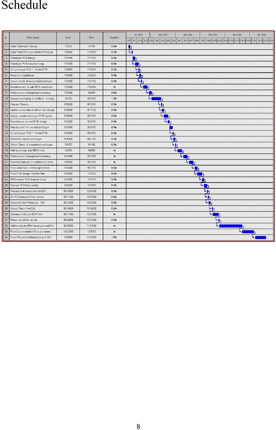
8 Schedule 8
9 Statement of work Initial Schematic Design Using OrCAD Capture 9.0 or the latest version available an initial schematic will be developed with only the core components of the design. The NETLIST will be generated using Tango format which Protel Advanced Schematic/PCB development packages requires. This technique is desirable since it allows a quick prototyping and turn around time using the T-Tek milling machine, which is available at In-Phase Technologies facilities. Initial Parts Procurement for Prototype The core components, which include the Synergy Synthesizer module and Hy-Q s VCXO 20 MHz frequency reference source, necessary to implement the design, will be ordered and stored in ESD (Electro-Static Discharge) safe bags until production and assembly of the prototype unit begins. Lead-time on these components should be less than a week and will not hold up the prototyping of the programmable frequency synthesizer s schedule. Prototype PCB design Protel Advanced Schematic/PCB development package will be utilized to complete the initial PCB layout necessary for the prototyping of the synthesizer. The components, which will be used, are mostly SMT (Surface Mount Technology) and the footprints can be created in Protel with little effort if they are unique. Importing OrCAD Capture s generated NETLIST file, which has been created in the Tango format, will be necessary. This technique has been determined in previous PCB design efforts to work correctly and will be applied here to limited unnecessary risk. Prototype PCB manufacturing 9

10 The file completed in Protel Advanced Schematic/PCB and exported correctly will be ready for importing into IsoPro software for modifications and additions before the final step of milling using the QuickCAM software and the T-TEK machine. Isopro uses the image files generated from Protel Advanced Schematic/PCB, which are in Gerber format, to create the layout in a way that QuickCAM understands. After exporting the files necessary and importing them into QuickCAM the prototype PCB will be manufactured. The three main limitations to the manufacturing of a PCB using the T-TEK machine are: (1) two -sided boards or single sided boards can be created but not three layers or greater. This design can easily be developed using a two-sided PCB as the basis. (2) The space between two traces is limited to the smallest end mill available which is.011 inch in diameter. (3) Vias or through-holes are limited to a diameter size of.011 inch. With these limitations in mind the PCB design can be manufactured very quickly. QC prototype PCB / Clean PCB The use of the T-TEK machine to produce a fast turn around PCB does not eliminate the need to QC (Quality Check) and clean the finished product. When milling has finished there are times that small fragments of copper clad still remain between traces or pads, which have, in past designs, created shorts to ground or undesired connections. The time spent verifying these issues making sure they are non-existent will, in the long run, save schedule delays with the elimination of time spent troubleshooting a unit with problems. Using alcohol and a cotton swab allows quick cleaning of the PCB. This makes the assembly and soldering of components easier and manufacturing problems become easy to see. Assembly of prototype Using good ESD procedures and wrist strap for a good ground, the components will be placed on the PCB and soldered. The small SMT components may require soldering to be performed under a microscope to insure proper soldering with no cold solder joints or solder bridges to other traces. The microscope, if necessary, is available at In-Phase Technologies and can be accessed to perform the soldering. Circuit check of assembled prototype 10
 two -sided boards or single sided boards can be created but not three layers or greater.")
11 The use of a digital multimeter set to measure ohms (continuity) will allow the circuit check to be performed. Using the schematic diagram generated in OrCAD Capture 9.0 and Protel Advanced Schematic/PCB layout/silkscreen a continuity check can be performed from point to point to verify the connections exist. This check again saves time in the long run and limits the loss and overstress of expensive components due to reverse biasing, improper voltage levels being applied to a pin, or connection not originally intended being made. Development of LabVIEW code/proto Once the prototyped programmable software controlled synthesized frequency source has been assembled and circuit checked it can be setup and used to help in the development of the LabVIEW VI (Virtual Instrument) necessary to control the hardware. The initial development will include a front panel display, which will have programming input fields available to the user for inserting various values to determine the dynamics of the prototype. Interfacing the DIO 96 card and terminal block to the hardware will require a test harness to connect the signals LabVIEW will control and supply to the unit. Using this setup, the initial code will be developed, allowing the testing of the hardware. Performance testing/troubleshooting With the use of the VI software developed in the previous stage, some basic tests will be performed to determine the need of additional circuitry. There are some main areas, which will be examined, to determine these needs. The lock detect output, which indicates a lock on frequency condition, will be looked at to verify a high or low logic level. Then, using a spectrum analyzer, the carrier frequency spectrum will be examined to verify again that it is locked to the correct frequency. Following this test, the output power of the synthesizer module will be determined, using the peak search feature on the spectrum analyzer, and compared to the specifications on the manufacturers data sheet. Then, locating the reference spurious frequencies, the determination of their power level as compared to the carrier frequency will be determined. This can be accomplished by peaking to the carrier frequency; then, using the marker delta feature, picking the peak on the reference spurs, and then comparing it to the data sheet to see if it meets the manufacturer s specifications. Phase noise measurements can be done next to verify they meet the manufacturers specifications. Using the HP8563E spectrum analyzer, property of In-Phase Technologies, there are two techniques that can be implemented to do this measurement. The first option is to use the built in USER program add-on to do the measurement. Using the first can also produce the degrees RMS measurement. The 11

12 second is the manual technique of verifying the phase noise by setting the span to a value that is large enough to move the marker 10KHz/100KHz off the carrier frequency and measuring the power level at that point. Another test that will be performed is the sensitivity of the VCXO. Controlling the Vt signal using LabVIEW will accomplish this by measuring the change in the output frequency as the DC level is varied. This test is necessary to determine the maximum swing of the reference source. The currents will be measured using the digital multimeter so that they are known for possible circuit design development. Using the oscilloscope, all signals will be monitored and examined to determine which signals may need signal conditioning. Design/prototyping of additional circuitry When additional circuitry is determined necessary Pspice will be used, where possible, to simulate the design of the additional circuitry. With the knowledge gained from other design efforts, the process should flow smoothly. Research, if needed, will be done to locate the necessary components. With the use of a Digi-Key catalog, along with many other sources, this task can be accomplished. Update schematic to reflect new design Documentation control will be maintained and the original OrCAD Schematic will be updated as the design matures and will reflect the most recent design. The NETLIST that is created with the schematic file will be regenerated so that the layout in Protel Advanced Schematic/PCB can be updated to incorporate the changes in the design. Design second prototype PCB layout Using Protel Advanced Schematic/PCB, the new footprints will be generated in the library. When the NETLIST is imported again the old layout will be modified and the added component will be loaded into this file so the layout can be modified to represent the current design. Manufacture second PCB design 12

13 When the Gerber files have been generated using Protel Advanced Schematic/PCB the same procedure used in the first prototyping unit will be used again to import them into IsoPro. Next it will be necessary to modify and then export the files in the QuickCAM format. The exported IsoPro files will then be imported into QuickCAM and the PCB can finally be milled and cutout yielding the new prototyping PCB. Procure parts for second prototype When the new design has been simulated using Pspice, or other simulation software, such as Matlab 5.0 or Touchtone, and a great degree of confidence with little risk exist the necessary parts will be procured. The main vendors that will be used as the sources of components are as follows: Digi-Key, Hy-Q, Newark Electronics and Compaq. QC prototype PCB / Clean PCB The use of the T-TEK machine to produce a fast turn around PCB does not eliminate the need to QC and clean the finished product. When milling has finished there are times that small fragments of copper clad still remain between traces or pads, which have, in past designs, created shorts to ground or undesired connections. The time spent verifying these issues making sure they are non-existent will, in the long run, save schedule delays with the elimination of time spent troubleshooting a unit with problems. Using alcohol and a cotton swab allows quick cleaning of the PCB. This makes the assembly and soldering of components easier and manufacturing problems become easy to see. Assemble second prototype Using good ESD procedures and wrist strap for a good ground, the components will be placed on the PCB and soldered. The small SMT components may require soldering to be performed under a microscope to insure proper soldering with no cold solder joints or solder bridges to other traces. The microscope, if necessary, is available at In-Phase Technologies and can be accessed to perform the soldering. Circuit Check of assembled prototype 13

14 The use of a digital multimeter set to measure ohms (continuity) will allow the circuit check to be performed. Using the schematic diagram generated in OrCAD Capture 9.0 and Protel Advanced Schematic/PCB layout/silkscreen a continuity check can be performed from point to point to verify the connections exist. This check again saves time in the long run and limits the loss and overstress of expensive components due to reverse biasing, improper voltage levels being applied to a pin, or connection not originally intended being made. Add necessary LabVIEW code Once the prototyped programmable software controlled synthesized frequency source has been assembled and circuit checked it can be set up and used to help in the additional development of the LabVIEW VI necessary to control the hardware. The development will include modification to front panel display, which will have the programming input fields available for inserting various values to determine the dynamics of the prototype. Additional interfacing of the DIO 96 card and terminal block to the hardware might require modifications to the test harness, which connects the signals LabVIEW will control and supply to the hardware. Using the hardware setup, and code developed will allow debugging of the new code and additional testing of the hardware. Performance testing/troubleshooting With the use of the VI software developed in the previous stage, the basic tests will be performed again to determine the need of additional circuitry. There are some main areas, which will be examined to determine these needs. The lock detect output, which indicates a lock on frequency condition, will be looked at to verify a high or low logic level. Then, using a spectrum analyzer, the carrier frequency spectrum will be examined to verify that it is locked to the correct frequency. Following this test, the output power of the synthesizer module will be determined, using the peak search feature on the spectrum analyzer, and compared to the specifications on the manufacturers data sheet. Then locating the reference spurious frequencies, the determination of their power level as compared to the carrier frequency will be determined. This can be accomplished by peaking to the carrier frequency then, using the marker delta feature, picking the peak on the reference spurs and comparing it to the data sheet to see if it meets the manufacturer s specifications. Phase noise measurements can be done next to verify they meet the manufacturer s specifications. Using the HP8563E spectrum analyzer, property of In- Phase Technologies, there are two techniques that can be implemented to do this measurement. The first option is to use the built in USER program add-on to do the 14

15 measurement. Using the first can also produce the degrees RMS measurement. The second is the manual technique of verifying the phase noise by setting the span to a value that is large enough to move the marker 10KHz/100KHz off the carrier frequency, measuring the power level at that point. Another test that will be performed is the sensitivity of the VCXO. Controlling the Vt signal, using LabVIEW, will accomplish this by measuring the change in the output frequency as the DC level is varied. This test is necessary to determine the maximum swing of the reference source. The currents will be measured using the digital multimeter so that they are known for possible circuit design development. Using the oscilloscope, all signals will be examined to determine if visible improvements have occurred on those signals that had problems in the prior prototype. The signals that still may need signal conditioning will be examined again and a new design approach will be taken to improve the performance. Possible redesign or additions to proto If the need of additional circuitry is determined, Pspice will be used, where possible to simulate the design of the additional circuitry. With the knowledge gained from other design efforts, the process should flow smoothly. Research if needed, will be done to locate the necessary components and with the use of a Digi-Key catalog, along with many other sources, this task can be accomplished. This should bring the design and layout closer towards the final EM. Final schematic / NETLIST generation Documentation control will be maintained and the original OrCAD Schematic will be updated to refelect the final design. The final NETLIST will be generated using the schematic file so that the final PCB layout in Protel Advanced Schematic/PCB can be designed making sure to incorporate all changes made to the previous design. Final PCB design / Gerber files Protel Advanced Schematic/PCB will be used to create the final Gerber files necessary to have a vendor manufacture the final PCB. Great care will be taken to ensure all layout problems have been fixed and are non-existent in the final PCB layout. The final dimensions must correspond to the dimensions specified to the chassis vendor. The main 15

16 landmarks include the output SMA connector and the side rail hole indexes which will be used to mounted the PCB securely and supply the PCB with a solid ground. RFQ various PCB manufactures There are a variety of vendors that can be used to produce the PCB from Gerber file format. The approach that will be used here is finding the manufacturer, which will produce the PCB for a competitive price and have a quick turn around on the design. One possible vendor is Advanced Circuit Inc. Based upon previous PCB design experience, it has been found that they are very helpful and try their best to turn the design into a PCB as quickly as possible. Although this vendor has been used in the past at In-Phase Technologies, other vendors will receive a RFQ (Request for Quote) and the decision will be made on which one to select, depending on their response. Procure PCB from vendor When the vendor has been selected, the PCB will be ordered and, depending on the way the schedule on the project is going, the amount of time set aside for delivery of the final EM PCB will be determined. The fact that In-Phase Technologies has prior dealings with most PCB vendors should make it possible to expedite the shipment if necessary. Procure final components for EM Components will be procured for the final prototype EM. Most of the components will be obtained from prior prototyping units to save cost. Some SMT parts are available at In- Phase Technologies and have no delivery times associated with them. Those that will need procurement will be ordered and delivery times will be minimized as much as possible to keep the project schedule flowing smoothly. QC PCB procured from vendor 16

17 The use of an outside source to produce a fast turn around PCB does not eliminate the need to QC (Quality Check) and clean the finished product. When PCBs are manufactured there can still be situations where traces connected to other traces or ground planes have created shorts to ground or undesired connections. The time spent verifying these issues making sure they are non-existent will, in the long run, save valuable resources with the elimination of effort spent troubleshooting a unit with problems. Using alcohol and a cotton swab allows the cleaning of the PCB. This makes the assembly and soldering of components easier and manufacturing problems become easy to see and proper actions can be taken to fix the problems. Assemble final Prototype - EM Using good ESD procedures and wrist strap for a good ground the components will be placed on the PCB and soldered. The small SMT components may require soldering to be performed under a microscope to insure proper soldering with no cold solder joints or solder bridges to other traces. The microscope, if necessary, is available at In-Phase Technologies and can be accessed to perform the soldering. With the EM design assembled the final results and performance can be studied. Circuit Check final EM The use of a digital multimeter set to measure ohms (continuity) will allow the circuit check to be performed. Using the schematic diagram generated in OrCAD Capture 9.0 and Protel Advanced Schematic/PCB layout/silkscreen a continuity check can be performed from point to point to verify the connections exist. This check again saves time in the long run and limits the loss and overstress of expensive components due to reverse biasing, improper voltage levels being applied to a pin, or connection not originally intended being made. Develop final LabVIEW GUI Once the EM prototype of the programmable frequency synthesizer has been assembled and circuit checked it can be set up and used to help in the additional development of the LabVIEW VI (Virtual Instrument) necessary to control the hardware. The development will include modification to front panel display, which will have the programming input 17

18 fields available for inserting various values to determine the dynamics of the prototype. Additional interfacing of the DIO 96 card and terminal block to the hardware may require modifications to the test harness which connects the signals LabVIEW will control and supply to the hardware. Using the hardware setup, the software developed will allow the final testing of verification of the unit as detailed in phase one of the design. Phase two of the design Depending on available time left in the schedule, phase two of the design will begin. Phase two consists of many small parts and a decision at this time will be made on the appropriate plan with a modified schedule, breaking down the details of the software development tasks to bring the new ideas into being. The main component of phase two of the project will require a variety of LabVIEW software development and interfacing. Additional LabVIEW development/gui In-Phase Technologies has developed LabVIEW software for the automation of STE (Special Test Equipment) and STA (Special Test Assemblies) chassis, which are designed and manufactured at the Clarksburg NJ location for a variety of customers. With the use of some already written LabVIEW code, the modifications and changes that will become clearly apparent at the time and necessary to implement the improvements, the additional LabVIEW software can be realized with little risk associated with it. The main driving force here is the ability to incorporate the changes and additions using the available scheduling time or the time gained in other areas of the project where tasks were completed ahead of schedule. Final Documentation/Test procedures The programmable frequency synthesizer will have a final documentation package associated with it, which will include schematics, PCB artwork, mechanical drawings, part list, LabVIEW front panel description explaining the display/controls and indicators, final test procedures to verify the unit works, with a step-by-step test to be performed at NJIT. Other documents may be contained in the final documentation package as it becomes necessary to include them. The contents of the package will also depend on if phase two is also completed 100% or partially. Final EM presentation/testing at NJIT 18

19 The final acceptance testing of the programmable software controlled synthesized frequency source will occur on a scheduled date at NJIT this date has not been set and is TBD (To Be Determined). The required hardware will be transported to the college and set up for the demonstration. In the event the demonstration spans overnight, the need to break down the setup and remove the high priced hardware will be necessary for security purposes as required by In-Phase Technologies management. The following day, the time required to set the test bed back up will be minimal. Dependent on whether phase two has been completed, the performance testing can be accomplished in about 20 minutes or less. 19

20 Budget In-Phase Technologies and the student will subsidize the design and devopment of the programmable software controlled synthesized frequency source. The project, not including test equipment, pc and DIO 96 card should not cost more than 500 dollars. The test equipment, pc, and DIO 96 card will be borrowed when the final acceptance testing occurs at NJIT. This project is a sub-system of the larger system, which will be delivered to USA. This sub-system will be designed and developed at work, but certain phases will be done at other times, if the schedule is behind or other projects require work. The final completion date should remain sound but the intermediate schedule from week to week may differ slightly as priorities arise. When these situations arise, late night sessions or weekend sessions will be implemented to keep the project on course. 20

21 21
22 Appendix Attached on the following pages are component data sheets and other helpful papers. 22
23 Bibliography Hy-Q International Synergy Microwave Corporation 23
Executive Summary. Table of Contents
 Executive Summary How to Create a Printed Circuit Board (PCB) Department of Electrical & Computer Engineering Michigan State University Prepared by: John Kelley Revision: 4/06/00 This application note
Prototyping Printed Circuit Boards
 Prototyping Printed Circuit Boards From concept to prototype to production. (HBRC) PCB Design and Fabrication Agenda Introduction Why PCBs? Stage 1 Understanding the rules Stage 2 Planning the board. Stage
HP 8970B Option 020. Service Manual Supplement
 HP 8970B Option 020 Service Manual Supplement Service Manual Supplement HP 8970B Option 020 HP Part no. 08970-90115 Edition 1 May 1998 UNIX is a registered trademark of AT&T in the USA and other countries.
IIB. Complete PCB Design Using OrCAD Capture and PCB Editor. Kraig Mitzner. ~»* ' AMSTERDAM BOSTON HEIDELBERG LONDON ^ i H
 Complete PCB Design Using OrCAD Capture and PCB Editor Kraig Mitzner IIB ~»* ' AMSTERDAM BOSTON HEIDELBERG LONDON ^ i H NEW YORK * OXFORD PARIS SAN DIEGO ШШЯтИ' ELSEVIER SAN FRANCISCO SINGAPORE SYDNEY
Laboratory 2. Exercise 2. Exercise 2. PCB Design
 Exercise 2. PCB Design Aim of the measurement Introducing to the PCB design Creating a schematic of an analog circuit, making simulations on it and designing a Printed circuit board for it. Keywords Printed
Analog Devices Welcomes Hittite Microwave Corporation NO CONTENT ON THE ATTACHED DOCUMENT HAS CHANGED
 Analog Devices Welcomes Hittite Microwave Corporation NO CONTENT ON THE ATTACHED DOCUMENT HAS CHANGED www.analog.com www.hittite.com THIS PAGE INTENTIONALLY LEFT BLANK PLL & PLL with Integrated VCO Evaluation
EECAD s MUST List MUST MUST MUST MUST MUST MUST MUST MUST MUST MUST
 Customers are required to follow certain criteria for all designs whether they are ultimately done in EECAD or by the customers themselves. These criteria, approved by EES Management, are listed below:
IC 1101 Basic Electronic Practice for Electronics and Information Engineering
 7. INDUSTRIAL CENTRE TRAINING In the summer between Year 1 and Year 2, students will undergo Industrial Centre Training I in the Industrial Centre (IC). In the summer between Year 2 and Year 3, they will
Analog Devices Welcomes Hittite Microwave Corporation NO CONTENT ON THE ATTACHED DOCUMENT HAS CHANGED
 Analog Devices Welcomes Hittite Microwave Corporation NO CONTENT ON THE ATTACHED DOCUMENT HAS CHANGED www.analog.com www.hittite.com THIS PAGE INTENTIONALLY LEFT BLANK Typical Applications The HMC547LP3
GRF-3300 RF Training Kits
 RF Training Kits Presenter : Cooper Liu, Engineer Department : Marketing & Service Division Date : Aug. 20, 2008 Educational challenges coped in RF circuits training Short of proper training tools The
Evaluation Board User Guide UG-127
 Evaluation Board User Guide UG-127 One Technology Way P.O. Box 9106 Norwood, MA 02062-9106, U.S.A. Tel: 781.329.4700 Fax: 781.461.3113 www.analog.com Evaluation Board for High Speed Op Amps Offered in
ERNI Systems USA Backplanes & Sub-Racks: Design, Simulation, Manufacturing and Test
 ERNI Systems USA Backplanes Sub-Racks: Design, Simulation, Manufacturing and Test www.erni.com Engineering From Beginning to End Conceptualization From Customer Idea to Statement of Work (SOW) Structuring
PCB Artist Tutorial:
 Derek Brower browerde@msu.edu Capstone Design Team 6 PCB Artist Tutorial: Printed Circuit Board Design Basics N o v e m b e r 1 4, 2 0 1 2 P C B B a s i c s P a g e 1 Abstract PCB Artist is a schematic
ICS379. Quad PLL with VCXO Quick Turn Clock. Description. Features. Block Diagram
 Quad PLL with VCXO Quick Turn Clock Description The ICS379 QTClock TM generates up to 9 high quality, high frequency clock outputs including a reference from a low frequency pullable crystal. It is designed
LEAN NPI AT OPTIMUM DESIGN ASSOCIATES: PART 1 WHERE ARE WE NOW? RANDY HOLT, OPTIMUM DESIGN ASSOCIATES JAMES DOWDING, MENTOR GRAPHICS
 W H I T E P A P E R LEAN NPI AT OPTIMUM DESIGN ASSOCIATES: PART 1 WHERE ARE WE NOW? RANDY HOLT, OPTIMUM DESIGN ASSOCIATES JAMES DOWDING, MENTOR GRAPHICS w w w. o d b - s a. c o m For more than twenty years,
Printed Circuit Boards. Bypassing, Decoupling, Power, Grounding Building Printed Circuit Boards CAD Tools
 Printed Circuit Boards (PCB) Printed Circuit Boards Bypassing, Decoupling, Power, Grounding Building Printed Circuit Boards CAD Tools 1 Bypassing, Decoupling, Power, Grounding 2 Here is the circuit we
Manufacturing Backend
 Manufacturing Backend Anusha Hiremath, Apoorva Dhavale, K V Roopa, Keertee Savadi, Aruna S. Nayak Computer Science and Engineering and Technology BVB College of Engineering and Technology Hubli, Karnataka,
Impedance 50 (75 connectors via adapters)
") VECTOR NETWORK ANALYZER PLANAR TR1300/1 DATA SHEET Frequency range: 300 khz to 1.3 GHz Measured parameters: S11, S21 Dynamic range of transmission measurement magnitude: 130 db Measurement time per point:
VECTOR NETWORK ANALYZER PLANAR TR1300/1 DATA SHEET Frequency range: 300 khz to 1.3 GHz Measured parameters: S11, S21 Dynamic range of transmission measurement magnitude: 130 db Measurement time per point:
Optimizing VCO PLL Evaluations & PLL Synthesizer Designs
 Optimizing VCO PLL Evaluations & PLL Synthesizer Designs Today s mobile communications systems demand higher communication quality, higher data rates, higher operation, and more channels per unit bandwidth.
INTELLIGENT INTERACTIVE SYNTHESIZER SURFACE MOUNT MODEL: MFSH615712-100
 SURFACE MOUNT MODEL: MFSH6572 65-72 MHz FEATURES: Small Size, Surface Mount (.6" x.6") Low Phase Noise Standard Programming Interface Ultra Wide Tuning Range Lead Free - RoHS Compliant Patented REL-PRO
How to make a Quick Turn PCB that modern RF parts will actually fit on!
 How to make a Quick Turn PCB that modern RF parts will actually fit on! By: Steve Hageman www.analoghome.com I like to use those low cost, no frills or Bare Bones [1] type of PCB for prototyping as they
Reverse Engineering: Printed Circuit Boards. Dr. Tarek A. Tutunji Philadelphia University, Jordan
 Reverse Engineering: Printed Circuit Boards Dr. Tarek A. Tutunji Philadelphia University, Jordan Reference PCB Reverse Engineering by John Armistead A Rapid Prototyping Methodology for Reverse Engineering
VJ 6040 Mobile Digital TV UHF Antenna Evaluation Board
 VISHAY VITRAMON Multilayer Chip Capacitors Application Note GENERAL is a multilayer ceramic chip antenna designed for receiving mobile digital TV transmissions in the UHF band. The target application for
Agilent N2717A Service Software Performance Verification and Adjustment Software for the Agilent ESA Spectrum Analyzers Product Overview
 Agilent N2717A Service Software Performance Verification and Adjustment Software for the Agilent ESA Spectrum Analyzers Product Overview Reduce your cost of ownership by minimizing time to calibrate and
Electronic Circuit Prototyping Techniques
 Electronic Circuit Prototyping Techniques Document Revision: 1.01 Date: February, 2007 16301 Blue Ridge Road, Missouri City, Texas 77489 Telephone: 1-713-283-9970 Fax: 1-281-416-2806 E-mail: info@bipom.com
DKWF121 WF121-A 802.11 B/G/N MODULE EVALUATION BOARD
 DKWF121 WF121-A 802.11 B/G/N MODULE EVALUATION BOARD PRELIMINARY DATA SHEET Wednesday, 16 May 2012 Version 0.5 Copyright 2000-2012 Bluegiga Technologies All rights reserved. Bluegiga Technologies assumes
Agilent P940xA/C Solid State PIN Diode Switches
 Agilent P940xA/C Solid State PIN Diode Switches Operating and Service Manual Agilent Technologies Notices Agilent Technologies, Inc. 2007 No part of this manual may be reproduced in any form or by any
APSYN420A/B Specification 1.24. 0.65-20.0 GHz Low Phase Noise Synthesizer
 APSYN420A/B Specification 1.24 0.65-20.0 GHz Low Phase Noise Synthesizer 1 Introduction The APSYN420 is a wideband low phase-noise synthesizer operating from 0.65 to 20 GHz. The nominal output power is
M. Jämsä 6.4.2011 PCB COST REDUCTIONS
 M. Jämsä 6.4.2011 PCB COST REDUCTIONS There is an old joke about Commodity Manager of PCB (Printed Circuit Board) having one brain cell only, either occupied by the idea of price reduction or by the idea
QUICK START GUIDE FOR DEMONSTRATION CIRCUIT 956 24-BIT DIFFERENTIAL ADC WITH I2C LTC2485 DESCRIPTION
 LTC2485 DESCRIPTION Demonstration circuit 956 features the LTC2485, a 24-Bit high performance Σ analog-to-digital converter (ADC). The LTC2485 features 2ppm linearity, 0.5µV offset, and 600nV RMS noise.
VCO Phase noise. Characterizing Phase Noise
 VCO Phase noise Characterizing Phase Noise The term phase noise is widely used for describing short term random frequency fluctuations of a signal. Frequency stability is a measure of the degree to which
Complete. PCB Design Using. NI Multisim, NI Ultiboard, LPKF CircuitCAM and BoardMaster. pg. 1. Wei Siang Pee
 Complete Wei Siang Pee PCB Design Using NI Multisim, NI Ultiboard, LPKF CircuitCAM and BoardMaster pg. 1 Introduction Multisim equips educators, students, and professionals with the tools to analyze circuit
Amplified High Speed Fiber Photodetectors
 Amplified High Speed Fiber Photodetectors User Guide (800)697-6782 sales@eotech.com www.eotech.com Page 1 of 7 EOT AMPLIFIED HIGH SPEED FIBER PHOTODETECTOR USER S GUIDE Thank you for purchasing your Amplified
AN-837 APPLICATION NOTE
 APPLICATION NOTE One Technology Way P.O. Box 916 Norwood, MA 262-916, U.S.A. Tel: 781.329.47 Fax: 781.461.3113 www.analog.com DDS-Based Clock Jitter Performance vs. DAC Reconstruction Filter Performance
Application Note: Spread Spectrum Oscillators Reduce EMI for High Speed Digital Systems
 Application Note: Spread Spectrum Oscillators Reduce EMI for High Speed Digital Systems Introduction to Electro-magnetic Interference Design engineers seek to minimize harmful interference between components,
AD9125-EBZ Quick Start Guide
 Quick Start Guide One Technology Way P.O. Box 9106 Norwood, MA 02062-9106, U.S.A. Tel: 781.329.4700 Fax: 781.461.3113 www.analog.com Getting Started with the Evaluation Board WHAT S IN THE BOX Evaluation
HOW PRODUCTS GET DESIGNED
 HOW PRODUCTS GET DESIGNED Introduction: This is a description of DFAD s role as an electronics design center, in designing products or projects for you. It also explains the interactions between all parties
Lab 3: Introduction to Data Acquisition Cards
 Lab 3: Introduction to Data Acquisition Cards INTRODUCTION: In this lab, you will be building a VI to display the input measured on a channel. However, within your own VI you will use LabVIEW supplied
THE R551N RECEIVER FAQ FAULT FINDING THE REDIFON COMMUNICATIONS RECEIVER R551N. Date: October 10th 1995 by: Jan Verduyn G5BBL
 THE R551N RECEIVER FAQ FAULT FINDING THE REDIFON COMMUNICATIONS RECEIVER R551N Introduction: Date: October 10th 1995 by: Jan Verduyn G5BBL Recently a number of Redifon R551N receivers have appeared on
Acceptability of Printed Circuit Board Assemblies
 Section No.: 12I.2.3, Sheet 1 of 9 Rev Level: 16 Additional Distribution: PCB Assembly Subcontractors 1.0 Purpose 2.0 Scope Acceptability of Printed Circuit Board Assemblies 1.1 The purpose of this standard
Milling Tools These are the tools currently available for use with the milling machine
 Jason Ward Page 1 of 5 Milling Tools These are the tools currently available for use with the milling machine T1 Milling Tool The missile-shaped T1 milling tools are the highest precision of T-Tech's milling
ISC Dual Frequency WFS RFPD Test Procedure:
 LASER INTERFEROMETER GRAVITATIONAL WAVE OBSERVATORY LIGO Laboratory / LIGO Scientific Collaboration LIGO 08 January 2013 ISC Dual Frequency WFS RFPD Test Procedure: Richard Abbott Distribution of this
Designing a Printed Circuit Board
 Designing a Printed Circuit Board Jamie Jacobs Design Team 4 4/03/2009 Abstract When the development stage of a circuit board is complete and working correctly, it is then necessary to take this breadboard
Switch board datasheet EB007-00-1
 Switch board datasheet EB007-00-1 Contents 1. About this document... 2 2. General information... 3 3. Board layout... 4 4. Testing this product... 5 5. Circuit description... 6 Appendix 1 Circuit diagram
Agilent N8973A, N8974A, N8975A NFA Series Noise Figure Analyzers. Data Sheet
 Agilent N8973A, N8974A, N8975A NFA Series Noise Figure Analyzers Data Sheet Specifications Specifications are only valid for the stated operating frequency, and apply over 0 C to +55 C unless otherwise
AMPLIFIED HIGH SPEED FIBER PHOTODETECTOR USER S GUIDE
 AMPLIFIED HIGH SPEED FIBER PHOTODETECTOR USER S GUIDE Thank you for purchasing your Amplified High Speed Fiber Photodetector. This user s guide will help answer any questions you may have regarding the
RF Power Amplifier PA10W Owner s Manual SpinCore Technologies, Inc. http://www.spincore.com
 RF Power Amplifier PA10W Owner s Manual SpinCore Technologies, Inc. http://www.spincore.com Congratulations and thank you for choosing a design from SpinCore Technologies, Inc. We appreciate your business!
Cumbria Designs T-1. SSB/CW Filter kit (4.9152MHz) User Manual
 User Manual") Cumbria Designs T-1 SSB/CW Filter kit (4.9152MHz) User Manual CONTENTS 1 INTRODUCTION 2 2 CIRCUIT DESCRIPTION 2 3 ASSEMBLY 2 4 TESTING 4 The Steading Stainton PENRITH Cumbria CA11 0ES UK 1 Introduction
Cumbria Designs T-1 SSB/CW Filter kit (4.9152MHz) User Manual CONTENTS 1 INTRODUCTION 2 2 CIRCUIT DESCRIPTION 2 3 ASSEMBLY 2 4 TESTING 4 The Steading Stainton PENRITH Cumbria CA11 0ES UK 1 Introduction
Analog Devices Welcomes Hittite Microwave Corporation NO CONTENT ON THE ATTACHED DOCUMENT HAS CHANGED
 Analog Devices Welcomes Hittite Microwave Corporation NO CONTENT ON THE ATTACHED DOCUMENT HAS CHANGED www.analog.com www.hittite.com THIS PAGE INTENTIONALLY LEFT BLANK v2.71 HMC42ST8 / 42ST8E AMPLIFIER,.4-2.2
PS6500 Storage Arrays Rack Mount Instructions
 PS6500 Storage Arrays Rack Mount Instructions Part Number: R724M Rev. A01 Copyright 2010 Dell, Inc. All rights reserved. Dell is a trademark of Dell, Inc. EqualLogic is a registered trademark. All trademarks
ICS650-44 SPREAD SPECTRUM CLOCK SYNTHESIZER. Description. Features. Block Diagram DATASHEET
 DATASHEET ICS650-44 Description The ICS650-44 is a spread spectrum clock synthesizer intended for video projector and digital TV applications. It generates three copies of an EMI optimized 50 MHz clock
RF Measurements Using a Modular Digitizer
 RF Measurements Using a Modular Digitizer Modern modular digitizers, like the Spectrum M4i series PCIe digitizers, offer greater bandwidth and higher resolution at any given bandwidth than ever before.
Interconnect Solutions For Global Technology
 The PHOENIX Company of Chicago TM Interconnect Solutions For Global Technology z RF/Microwave Cable Assemblies z Coax Connectors z Blind Mate Connectors z Integrated Products z Molded Cable Assemblies
HIGH REPEATABILITY, BROADBAND TO-5 RELAYS DPDT
 HIGH REPEATABILITY, BROADBAND TO-5 RELAYS DPDT SERIES RF00 RF00D RF00DD RF0 RF0D RF0DD RELAY TYPE Repeatable, RF relay Repeatable, RF relay with internal diode for coil transient suppression Repeatable,
Using CAD Data in Assembly - Advantages and Pitfalls
 Using CAD Data in Assembly - Advantages and Pitfalls For years, electronic engineers and circuit board designers have shared information between their computer-aided-engineering (CAE) and computer-aided-design
Connector Launch Design Guide
 WILD RIVER TECHNOLOGY LLC Connector Launch Design Guide For Vertical Mount RF Connectors James Bell, Director of Engineering 4/23/2014 This guide will information on a typical launch design procedure,
Electronics Technology
 Teacher Assessment Blueprint Electronics Technology Test Code: 5907 / Version: 01 Copyright 2011 NOCTI. All Rights Reserved. General Assessment Information Blueprint Contents General Assessment Information
Example #1: Controller for Frequency Modulated Spectroscopy
 Progress Report Examples The following examples are drawn from past student reports, and illustrate how the general guidelines can be applied to a variety of design projects. The technical details have
Embedded FM/TV Antenna System
 1 Embedded FM/TV Antenna System Final Report Prepared for By January 21, 2011 2 Table of Contents 1 Introduction... 5 2 Technical Specification... 6 3 Prototype Antenna... 7 4 FASTROAD Active module fabrication...
NBB-402. RoHS Compliant & Pb-Free Product. Typical Applications
 Typical Applications Narrow and Broadband Commercial and Military Radio Designs Linear and Saturated Amplifiers 0 RoHS Compliant & Pb-Free Product NBB-402 CASCADABLE BROADBAND GaAs MMIC AMPLIFIER DC TO
Teaching the Importance of Data Correlation in Engineering Technology
 Session 3549 Teaching the Importance of Data Correlation in Engineering Technology Michael R. Warren, Dana M. Burnett, Jay R. Porter, and Rainer J. Fink Texas A&M University Abstract To meet the needs
Current Loop Tuning Procedure. Servo Drive Current Loop Tuning Procedure (intended for Analog input PWM output servo drives) General Procedure AN-015
 General Procedure AN-015") Servo Drive Current Loop Tuning Procedure (intended for Analog input PWM output servo drives) The standard tuning values used in ADVANCED Motion Controls drives are conservative and work well in over 90%
Servo Drive Current Loop Tuning Procedure (intended for Analog input PWM output servo drives) The standard tuning values used in ADVANCED Motion Controls drives are conservative and work well in over 90%
Using Stencils to Simplify the Printed Circuit Board Assembly Process
 Using Stencils to Simplify the Printed Circuit Board Assembly Process Author: Nolan Johnson CAD/EDA Manager njohnson@sunstone.com The process of creating a prototype circuit board requires multiple phases
Designing the NEWCARD Connector Interface to Extend PCI Express Serial Architecture to the PC Card Modular Form Factor
 Designing the NEWCARD Connector Interface to Extend PCI Express Serial Architecture to the PC Card Modular Form Factor Abstract This paper provides information about the NEWCARD connector and board design
PCB Board Design. PCB boards. What is a PCB board
 PCB Board Design Babak Kia Adjunct Professor Boston University College of Engineering Email: bkia -at- bu.edu ENG SC757 - Advanced Microprocessor Design PCB boards What is a PCB board Printed Circuit Boards
QCJ5 precision prototyping system
 QCJ5 precision prototyping system QCJ5the intelligent solution - QCJ5 setting the NEW standard for in-house prototyping! 12, 24 or 32-Position Automatic Tool Change Projects run unattended and uninterrupted,
ECEN 1400, Introduction to Analog and Digital Electronics
 ECEN 1400, Introduction to Analog and Digital Electronics Lab 4: Power supply 1 INTRODUCTION This lab will span two lab periods. In this lab, you will create the power supply that transforms the AC wall
PLL Frequency Synthesizer Evaluation Kit. PE3293-EK User s Manual
 PLL Frequency Synthesizer Evaluation Kit PE3293-EK User s Manual 6175 NANCY RIDGE DRIVE, SAN DIEGO, CA 92121 (858) 455-0660, FAX (858) 455-0770 http://www.peregrine-semi.com 1 Table of Contents FCC Labeling
DRM compatible RF Tuner Unit DRT1
 FEATURES DRM compatible RF Tuner Unit DRT1 High- Performance RF Tuner Frequency Range: 10 KHz to 30 MHz Input ICP3: +13,5dBm, typ. Noise Figure @ full gain: 14dB, typ. Receiver Factor: -0,5dB, typ. Input
155 Mb/s Fiber Optic Light to Logic Receivers for OC3/STM1
 155 Mb/s Fiber Optic Light to Logic Receivers for OC3/STM1 Application Note 1125 RCV1551, RGR1551 Introduction This application note details the operation and usage of the RCV1551 and RGR1551 Light to
Rapid Audio Prototyping
 Rapid Audio Prototyping Rapid Audio Prototyping Do You want to combine research and prototyping in one step? Do You want to test and evaluate the audio processing chain of Your product idea already at
Joule Thief 3.0 Kit. June 2012, Rev 1 1 http://www.easternvoltageresearch.com Joule Thief 3.0
 Kit Instruction Manual Eastern Voltage Research, LLC June 2012, Rev 1 1 http://www.easternvoltageresearch.com HIGH BRIGHTNESS LED THIS KIT USES A 1W CREE, HIGH BRIGHTNESS LED. DO NOT STARE AT THIS (OR
Features. Modulation Frequency (khz) VDD. PLL Clock Synthesizer with Spread Spectrum Circuitry GND
 VDD. PLL Clock Synthesizer with Spread Spectrum Circuitry GND") DATASHEET IDT5P50901/2/3/4 Description The IDT5P50901/2/3/4 is a family of 1.8V low power, spread spectrum clock generators capable of reducing EMI radiation from an input clock. Spread spectrum technique
DATASHEET IDT5P50901/2/3/4 Description The IDT5P50901/2/3/4 is a family of 1.8V low power, spread spectrum clock generators capable of reducing EMI radiation from an input clock. Spread spectrum technique
Universal Vehicle Power Supply 9007AX01. Installation Instructions
 Universal Vehicle Power Supply 9007AX01 Installation Instructions Disclaimer Honeywell International Inc. ( HII ) reserves the right to make changes in specifications and other information contained in
Jitter in PCIe application on embedded boards with PLL Zero delay Clock buffer
 Jitter in PCIe application on embedded boards with PLL Zero delay Clock buffer Hermann Ruckerbauer EKH - EyeKnowHow 94469 Deggendorf, Germany Hermann.Ruckerbauer@EyeKnowHow.de Agenda 1) PCI-Express Clocking
LO5: Understand commercial circuit manufacture
 Unit 6: Circuit simulation and manufacture LO5: Understand commercial circuit manufacture Commercial component and PCB types Instructions and answers for teachers These instructions should accompany the
INSTRUCTION FOR COMPLETING COMPETITIVE SOLICITATION ACKNOWLEDGEMENT FORMS
 INSTRUCTION FOR COMPLETING COMPETITIVE SOLICITATION ACKNOWLEDGEMENT FORMS The Competitive Solicitation Acknowledgement Form must be completely filled in. This may be done on line then printed or you may
ZLPLL Local Oscillator
 ZLPLL Local Oscillator Wayne Knowles, ZL2BKC w.knowles@xtra.co.nz Contents 1 Introduction... 3 2 Specifications... 3 3 Performance... 4 3.1 Phase Noise... 4 3.2 Output Level... 4 3.3 Harmonic Level...
Application Note: PCB Design By: Wei-Lung Ho
 Application Note: PCB Design By: Wei-Lung Ho Introduction: A printed circuit board (PCB) electrically connects circuit components by routing conductive traces to conductive pads designed for specific components
Inverter Field Service Technician II
 Inverter Field Service Technician II This position requires extensive travel when in the field. When Inverter Field Service Technicians do not have field assignments they are assigned to the factory s
PRELIMINARY. J-Series High PDE and Timing Resolution, TSV Package. High-Density Fill Factor Silicon Photomultipliers. Overview
 High-Density Fill Factor Silicon Photomultipliers SensL s J-Series low-light sensors feature an industry-leading low dark count rate and a high PDE that extends much further into the blue part of the spectrum
This lab is due 5:30PM Tuesday November 2, 2010 at 115 Hackerman Hall
 M.E. 530.420 Lab 7: Printed Circuit Board Design Louis L. Whitcomb Department of Mechanical Engineering G.W.C. Whiting School of Engineering The Johns Hopkins University This lab is due 5:30PM Tuesday
Accelerometer and Gyroscope Design Guidelines
 Application Note Accelerometer and Gyroscope Design Guidelines PURPOSE AND SCOPE This document provides high-level placement and layout guidelines for InvenSense MotionTracking devices. Every sensor has
Harmonics and Noise in Photovoltaic (PV) Inverter and the Mitigation Strategies
 Inverter and the Mitigation Strategies") Soonwook Hong, Ph. D. Michael Zuercher Martinson Harmonics and Noise in Photovoltaic (PV) Inverter and the Mitigation Strategies 1. Introduction PV inverters use semiconductor devices to transform the
Soonwook Hong, Ph. D. Michael Zuercher Martinson Harmonics and Noise in Photovoltaic (PV) Inverter and the Mitigation Strategies 1. Introduction PV inverters use semiconductor devices to transform the
FM TRANSMITTER & RECEIVER HYBRID MODULES. FM-RTFQ SERIES FM-RRFQ SERIES. Transmitter. Receiver. Applications
 FM Radio Transmitter & Receivers Available as or or 868MHz Transmit Range up to 20m Miniature Packages Data Rate up to 9.6Kbps No Adjustable Components Very Stable Operating Frequency Operates from 20
Hard Disk Drive (HDD)
") Installation Instructions Hard Disk Drive (HDD) Catalog Number 6189V-35HDDST80, 6189V-35HDDST160 Topic Page About This Publication 1 Important User Information 2 Electrostatic Discharge (ESD) Precautions
Installation Instructions Hard Disk Drive (HDD) Catalog Number 6189V-35HDDST80, 6189V-35HDDST160 Topic Page About This Publication 1 Important User Information 2 Electrostatic Discharge (ESD) Precautions
Designing and Planning a Printed-Circuit Board (PCB) Prototype
 Prototype") Designing and Planning a Printed-Circuit Board (PCB) Prototype Min Chen, Student Member, IEEE, and Gabriel A. Rincón-Mora, Senior Member, IEEE Georgia Tech Analog and Power IC Design Lab School of Electrical
Designing and Planning a Printed-Circuit Board (PCB) Prototype Min Chen, Student Member, IEEE, and Gabriel A. Rincón-Mora, Senior Member, IEEE Georgia Tech Analog and Power IC Design Lab School of Electrical
Assembly of LPCC Packages AN-0001
 Assembly of LPCC Packages AN-0001 Surface Mount Assembly and Handling of ANADIGICS LPCC Packages 1.0 Overview ANADIGICS power amplifiers are typically packaged in a Leadless Plastic Chip Carrier (LPCC)
************* OWNER'S MANUAL BAMF800/2 BAMF1250/2 BAMF1800/2 BAMF2200/2 BAMF2600/2 BAMF1200/4 BAMF1600/4 BAMF2000/1D BAMF4000/1D BAMF5500/1D
 ************* OWNER'S MANUAL BAMF800/2 BAMF1250/2 BAMF1800/2 BAMF2200/2 BAMF2600/2 BAMF1200/4 BAMF1600/4 BAMF2000/1D BAMF4000/1D BAMF5500/1D INTRODUCTION Power Acoustik amplifiers provide high-performance
C8051F020 Utilization in an Embedded Digital Design Project Course. Daren R. Wilcox Southern Polytechnic State University Marietta, Georgia
 C8051F020 Utilization in an Embedded Digital Design Project Course Daren R. Wilcox Southern Polytechnic State University Marietta, Georgia Abstract In this paper, the utilization of the C8051F020 in an
SuperIOr Controller. Digital Dynamics, Inc., 2014 All Rights Reserved. Patent Pending. Rev: 5-16-14 1
 SuperIOr Controller The SuperIOr Controller is a game changer in the world of high speed embedded control. The system combines incredible speed of both control and communication with revolutionary configurable
TRIPLE PLL FIELD PROG. SPREAD SPECTRUM CLOCK SYNTHESIZER. Features
 DATASHEET ICS280 Description The ICS280 field programmable spread spectrum clock synthesizer generates up to four high-quality, high-frequency clock outputs including multiple reference clocks from a low-frequency
RF Network Analyzer Basics
 RF Network Analyzer Basics A tutorial, information and overview about the basics of the RF Network Analyzer. What is a Network Analyzer and how to use them, to include the Scalar Network Analyzer (SNA),
Improve PCB Layout with Skill Utility Programs
 Improve PC Layout with Skill Utility Programs rbel Nissan, COO, Nistec Design Published at PCD&F Magazine, May 2008 Faster time to market is crucial in the development and manufacturing of every new product.
A number of simulating software are also being used which include: Circuit board plotter for in-house RF and microwave board prototyping
 Printed circuit boards ( PCB ) are one of the most important parts of electrical and electronic devices. The increasing miniaturisation of integrated circuits, higher packing density and smaller layout-dimensions
The Don ts of Better Flexible Circuit Design and Manufacture By Mark Finstad Friday, 01 June 2007
 The Don ts of Better Flexible Circuit Design and Manufacture By Mark Finstad Friday, 01 June 2007 Successful designs are soon forgotten but failures are remembered for years. Steering clear of these twelve
Application Note 58 Crystal Considerations with Dallas Real Time Clocks
 www.dalsemi.com Application Note 58 Crystal Considerations with Dallas Real Time Clocks Dallas Semiconductor offers a variety of real time clocks (RTCs). The majority of these are available either as integrated
SingleNet Single Cable Control System
 Single Cable Control System Economical, Reliable and Expandable Two-Wire Single Cable System DRIP/MICRO IRRIGATION PRODUCTS Single Cable Control System System Manager or Irrigation Controller Controls
Powering Integrated Circuits (ICs), and managing ripple voltage as it relates
, and managing ripple voltage as it relates") Ripple Voltage & ESR Powering Integrated Circuits (ICs), and managing ripple voltage as it relates to ESR of capacitors Low voltage ICs require supply voltage (Vcc) to have reduced levels of ripple voltage
Ripple Voltage & ESR Powering Integrated Circuits (ICs), and managing ripple voltage as it relates to ESR of capacitors Low voltage ICs require supply voltage (Vcc) to have reduced levels of ripple voltage
Designing a Schematic and Layout in PCB Artist
 Designing a Schematic and Layout in PCB Artist Application Note Max Cooper March 28 th, 2014 ECE 480 Abstract PCB Artist is a free software package that allows users to design and layout a printed circuit