Some Notes on Using Protel Software for Schematic Capture and PCB Layout
|
|
|
- Cornelius Dorsey
- 8 years ago
- Views:
Transcription
1 Some Notes on Using Protel Software for Schematic Capture and PCB Layout The design of an electronic circuit is a mixture of engineering science, art, and common-sense. One must choose a circuit configuration, perform supporting calculations, and select actual electronic devices taking into consideration their characteristics, price and availability. The circuit may be prototyped, and/or circuit simulation may be performed. As in all design work, the design process is iterative you need to make initial selections based on your calculations, and then see if they work. Virtually all electronic circuits that are produced in volume are fabricated on printed circuit boards [PCBs, also called printed wire boards, PWBs]. With the introduction of relatively inexpensive ($2k- $10k), high-quality PCB layout software for personal computers, it is now also common for prototype and one-off circuits to be implemented as PCBs. When designing an electronic circuit, the selection of components and the physical layout of the circuit can, in some cases, be as important as the design of the circuit itself. An electronic circuit must be fabricated from real electronic devices. Real devices have non-zero physical size and fixed terminal positions and sizes. Real devices also have non-ideal electronic characteristics. Electromagnetic interference can be a significant problem, particularly for low-noise analogue circuits. Signals take a finite time to propagate along the electrical tracks which make the circuit connections. This can cause timing problems, particularly if the circuit board is large. At high frequencies (10s MHz-GHz), the conductive tracks behave as transmission lines, with signal reflections occuring where circuit impedence changes abruptly. Although these effects usually become important for circuits which must operate with very low noise, or at high frequency (above 20MHz, say), it is important to appreciate of some of the practical problems encountered in circuit layout. 1 An Overview of Circuit Design and PDB Layout 1.1 Circuit Schematic Drafting A schematic of the circuit is usually sketched first by hand, in order to define the concept and topology of the circuit. As the design is refined, perhaps with the aid of calculations and circuit simulation together with information on the price and availability of components, the circuit is often drawn on a personal computer or workstation using a schematic editor. This approach has many advantages: the circuit can be drawn in a standardised, clear and neat way which promotes understanding; changes to the component parts or connections can easily be made; some checking of the design can be done automatically for example, a connection that consists only of output pins is probably wrong! the circuit can be exported to a circuit simulation program such as PSpice; a netlist that defines the circuit parts and interconnections can be created for export to a PCBlayout program; a bill of materials can be created, from which parts can be ordered. One important advantage of this approach is that a netlist file can automatically be created. A netlist is simply a list of all of the parts and connections in the circuit. Each net is one electrically continuous connection: for example, all pins that are connected to +5V form one net which is usually designated VCC. When laying out the circuit, the netlist can be imported into a PCB-layout program. The PCB- 1 of 10

2 layout program uses the connectivity information in the netlist, which helps to prevent connection errors during manual or automatic track routing. The bill of materials (BOM) is a convenient list from which the components may be ordered. 1.2 An Overview of PCB Design and Fabrication Once the electronic circuit is drawn by hand, or using a schematic editor, the board layout can begin. Board layout begins by deciding where to place the components on the board. Placement is usually the most important and difficult step in the layout. Next, place the tracks to complete the circuit. Track routing can be done in a number of different ways. The easiest, and often the best for simple circuits, is to use pencil and 5mm squared paper. Note that many through-hole components have their terminals arranged on a standard 0.1 grid. A PCB layout program can be used for manual track placement ( pad-to-pad routing ), or an autorouter can be used if this facility is provided by the PCB layout software. A netlist produced by circuit drafting software is often a great help in reducing connection errors when moving from the schematic to a finalised board layout. Once the layout is complete, the board can be fabricated. In commercial production, this is a complicated and involved process that involves a large number (100+) of separate photographic and electrochemical processes, together with cutting, drilling, plating, tinning, printing, and testing Hand-made PCBs With a little 1 practice and the correct, fresh materials, simple printed circuit boards can be made by hand. With careful registration of the layers, double-sided boards can be made. It is not practical to make plated-through holes (PTH), so vias ( vertical connections between layers) must be made by hand-soldering wire links or pins ( matrix pins ) through a board. If multi-layer boards (commercial boards may have up to up to 12 conductor layers) with plated-through holes are needed, they will need to be fabricated by a commercial PCB manufacturer. A simplified production process could begin with laser printing a positive image of the tracks onto transparent film, and then photographically transferring the image onto reversal film to make a negative image. This negative is contact-printed onto commercial photo-sensitive coper-clad board that has been pre-coated with a photoresist material. To maintain the best image quality, contact printing is done with the film emulsion pressed onto the photoresist using glass plates. The photoresist is exposed to UV light for seconds, depending on the light intensity. The positive image of the tracks hardens during photographic developing, and the remainder of the resist can be washed off, exposing the copper layer. All copper which is not protected by the resist layer is then chemically etched away, leaving the copper tracks. The photoresist is then stripped, and the board is trimmed and drilled by hand. Before soldering, the copper should be well cleaned (scrubbing with Ajax works well), and the boards should be sprayed with PCB lacquer. The lacquer will prevent the copper from tarnishing, and can be soldered-through. All that remains is to insert the components ( stuff the board), to solder them into the circuit, and to test the completed circuit. Then you can revise the design, re-do the board layout, make the second prototype board, etc Circuit and PCB Software We have licences for a schematic capture program Advanced Schematic and a companion PCB layout program Advanced PCB. Both programs were written by an Australian company, Protel 2 Pty. Ltd. Altium produces some of the world s most advanced PC-based electronic design automation (EDA) tools. Although our licences are for obsolete versions of the programs, they are adequate for simple design tasks. Full documentation available as on-line help from within the programs, and some brief suggestions for circuit drafting are appended to these notes. Your design should be based around components that are commonly available from electronics hobby stores: 1 A practice little is OK; a lot is much better 2 Now Altium Ltd. 2 of 10

3 David Reid Electronics, Jaycar Electronics, Dick Smith Electronics, or component distributors such as: Farnell RS Components The three hobbyist suppliers listed are all in York Street, Sydney take the train 3 to Town Hall Station. Component price and availability should be considered when choosing between alternatives. 2 Editing Circuit Diagrams with Advanced Schematic 2.1 Starting the Program Start the program from All Programs > Eng > CAD > Protel, and make a new schematic (.sch) file in your file space. 2.2 Part Placement A part can only be placed if the library that contains the part is loaded. Each parts library is equivalent to a manufacturer s data book. Use Library > Add/Remove (shortcut is L A) to load a library. A useful library to load is device.lib; it contains common devices such as resistors, capacitors, connectors, etc. The libraries d_something.lib are for compatibility with the DOS version of Schematic and should not be used. Place a part by Place > Part (shortcut is P P). Then type in the component identifier. Note that some parts are identified by manufacturer as well as generic part name: the identifier 7400 for a TTL NAND gate is incorrect, but DM7400 is satisfactory. DM is one of the prefixes used by National Semiconductor. The book by Horowitz & Hill contains a big list of manufacturers prefixes. Alternatively, a part can be placed from within the Component Browser. Open the Component Browser by Options > Component Browser (shortcut is O B). Choose the appropriate library and find the part by browsing. Component types are conventionally designated by letters. The Australian standard designators are : A Assembly, such as an IC, amplifier, box of tricks, etc. C Capacitor D Digital device - typically an IC F Protective device (e.g. fuse) L Inductor R Resistor S Switch V Semiconductor (transistor, diode, etc.) X Connector or terminal For example, R26 would be a resistor. See SAA HB for more information. Quite often, U is used to designate an IC, and D is used to designate a diode. Some parts, such as the simple TTL gates, have multiple devices within a single part. The individual devices are designated as U2:A, U2:B, etc. That is, U2:A is device A in part U2. U2:B is the second device (gate) in the part U1.. Change the part designator generated by Protel from (for example) U? to U1. The next U part to be placed will then automatically be designated U2 When placing a part, you can edit at placement (when the part outline is shown, indicating that the part can be dragged) by pressing the TAB key. Otherwise, edit a placed part by double clicking it. During placement, SPACEBAR will rorate a part, X or Y will flip it. 3 But make sure that you give it back. 3 of 10
 file in your file space. 2.")
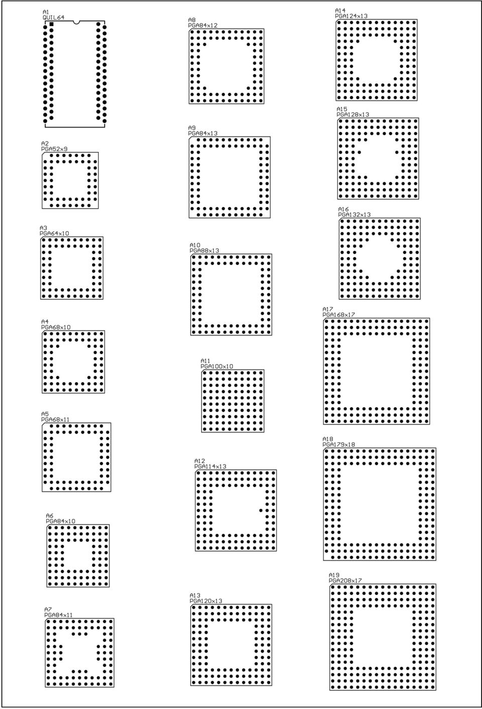
4 Don t forget to place connectors to allow you to get power and signals into and out of your board! 2.3 Footprints The footprint is the physical size, outline, pin location and size, etc. of a part. Some parts have multiple footprints that are defined in Protel s PCB libraries. For example, a DM74LS00 NAND gate can be supplied in a through-hole DIP14 package, or in a surface-mount SOIC14 package. Other parts, such as resistors, capacitors and switches, have no standard footprint, and so do not have a footprint defined in the libraries. If the schematic is going to be used as the basis for a PCB design, you will need to enter an appropriate footprint into the part s footprint field at part placement. Some useful footprints defined in the Advanced PCB footprint library are shown in the appendix to these notes Predefined Footprints Note Protel s names of the standard footprints, which are defined in PFW.LIB. Open this file from within Advanced PCB by using Library > Components to see all the pre-defined footprints. If a footprint that you need is not defined, you will have to create it using Library > Components. Note that Protel s footprints have been known to be wrong. If you are going to build the board, it is imperitive that every footprint be checked against the component manufacturers specifications User Defined Footprints If a part (e.g. an unusual IC) or component package (e.g. a switch) that you need to use is not defined in Protel s libraries, you will have to define it yourself using the Library > Run Library Editor command from within Advanced Schematic. It is good practice to make pin 1 on each component square for ease of identification; the component footprints (or patterns ) provided by Protel follow this convention. Note that inch measurements are commonplace in PCB work. Most older components have pins which are on a standard (100 mil) grid. One thousandth of an inch is invariably called a mil in PCB work. The size of a pin is not standardised. 2.4 Place Wires Once two or more parts are placed on the schematic, place wires to connect up the pins of parts to complete the circuit. Shortcut is P W. A junction (red dot) indicates that crossing wires are joined. A wire that starts from the end of another wire will be joined to it electrically. Make sure that wires that should not be electrically joined do not have a junction at their crossing point. 2.5 Net Labels, and Power Pins Sometimes a circuit diagram can become messy or confusing if every connection is drawn. Instead of drawing some of the wires in their entirety, a short wire can be drawn from each pin on the net, and a net label added to each short wire. Although there is no wire drawn between pins, the pins are electrically connected via the net label. Use Place > Net label (shortcut is P N) to place a net label. Parts in the Protel schematic libraries may have hidden power pins that are automatically connected to the nets VCC (+5 Volts) and GND (+0 Volt digital ground). This convention applies particularly to TTL chips 4, where the power connections are seldom shown on the schematic. Protel allows you to view the hidden pins, and follows the convention that if you un-hide a hidden pin you have to manually make a connection to it. 2.6 Wiring Tool Bar Most of the tools needed for placing parts, wires, net labels, etc. are available on the wiring toolbar. (shortcut is O W). Use edit at placement to get variants. 4 74xxxx family parts have power supply at the top right pin, and ground at bottom left. 4 of 10

5 2.7 Check the Circuit Protel has a tool called the electrical rules check (ERC) that checks the connections in your circuit against some logical errors, such as a net that only contains output pins. Run it by File > Reports > Electrical Rules Check (shortcut is F R E). Eliminate all of the errors. You can also highlight the connections on any particular net by Edit > Select > Net (shortcut is E S N). To unselect, do by Edit > Unselect > All (shortcut is E E A). 2.8 Netlist and Bill of Materials Can be generated from File > Reports. The netlist is required for importation into a PCB-layout program. 3 PCB Layout with Advanced PCB If you plan on making a PCB by hand, design your board using so-called 100 mil (or ) through-hole technology: grid for pin placement 100 mils (2.5 mm); routing grid 25 mils (0.6 mm); minimum track width 12 mils (0.3 mm); minimum track to track clearance 12 mils (0.3 mm); minimum pad size 65 mils (1.6 mm); minimum via size 50 mils (1.3 mm); only one track between pads. Remember, 1 mil is inch, or mm. 3.1 Starting the Program Start the program from All Programs > Eng > CAD > Protel. The first thing that you need to do is to get all of the component footprints on the board, and in the best relative positions. 3.2 Netlist Netlist Load will load the netlist specified, and import the footprints (patterns) associated designated for each part. Note that a component footprint will be found only if the footprint library containing it is loaded at the time the netlist is loaded. After the load, there should be no missing patterns, components or pins. All components will be placed on top of each other. Select the components, then centre them on your board area. Use Auto > Placement Tools > Expand Horizontal and Expand Vertical to spread out the components. Then use Netlist > Optimise > All to re-order the nets in an optimal (shortest path) way. Next, move the components around to get the best layout. This is the most critical step of the layout. Don t bother with Auto Place, as it runs very slowly and cannot outperform manual placement. Some guidelines that you should follow in placing parts are: Don t forget that you have to mount the board mechanically somehow. M3 machine screws are often used, so place four pads of diameter 6.0 mm and 3.5 mm hole size in the corners of the board. place components so that the track routes are short and as straight as possible; place components as close together as possible; but leave sufficient room between components to get the tracks in; all ICs should face the same way, say pin 1 at top left. Line up components in rows; place connectors, adjustment pots, switches and diagnostic LEDs at or near the board edges. 5 of 10

6 Repeat the Netlist > Optimise and component moving steps until you think that the placement is satisfactory. 3.3 Board Dimensions Have a guess at the board size - be generous with the size when you begin, as a board that is too small will make track routing very difficult. Place a closed rectangle of purple keep-out layer track to define the board limits. The keep-out layer is required for the Auto-router to run. 3.4 Track Routing Set up the routing clearances, using Netlist > Clearances. For technology, set all clearances to 5 mil. Then, set up the auto router by Auto > Setup Auto Route. Choose, for technology routing grid: 25 mil; track width: 12 mil; via size: 50 mil; via hole: 28 mil; Set hugging before 100% (completion), spreading after 100%; Select only the memory and line-probe router passes at this stage. Use Auto > Move to Grid to juggle the components a little bit so that their pins line up with the routing grid. This step is important, and can have a large effect on the completion percentage. Make sure that the grid that you move to is the same dimension as the grid selected for routing, usually 20 or 25 mil. Then save the board before any track routing is done. Then run the auto router, by Auto > Auto Route > All. Then, remove the memory and line-probe passes, and add (say) one maze and one smoothing pass. Run the auto router again. Continue until the board is routed satisfactorily, or you decide to give up and re-do the component placement and board size. You might want to save the board with a slightly different name after each routing pass. It is important to note that auto-routing is very definitely an iterative manual design process. The quality of the final result depends entirely on the component placement, the track width, pad and via sizes chosen, the clearances chosen, the router passes selected, and the number and order of the passes. You will have to do a number of layouts to get a reasonable design. It will always be necessary to clean up the routed board by hand after the auto router has finished. 6 of 10

7 References. Airborne Electronics: - Information on circuit design and PCB layout.. BEC Manufacturing: - Information on PCB layout.. Precision Circuits: a very good set of customer information documents for PCB design and manufacturing.. SAA HB3-1986: Electrical and Electronic Drawing Practice for Students. Standards Association of Australia, Sydney, Coombs, C.F. (ed.) Printed Circuits Handbook. 3ed., McGraw-Hill, Ginsberg, G.L. Printed Circuits Design. McGraw-Hill, New York, /6 Hall, D.V. Microprocessors and digital systems. 2ed., McGraw-Hill, Singapore, /44 Horowitz, P. and Hill, W. The Art of Electronics. 2 ed., CUP, Cambridge, Jung, W.G. IC OP-Amp Cookbook. 3ed., Howard Sams, Indianapolis, Lancaster, D. TTL Cookbook. Howard Sams, Indianapolis, Lancaster, D. CMOS Cookbook. Howard Sams, Indianapolis, Noble, P.J.W. Printed Circuit Board Assembly. Chapman & Hall, London, Phillips, G. Newnes Electronics Toolkit. Newnes, Oxford, Williams, T. Circuit Designer s Companion. Butterworth, Kent, /118 Appendix: Footprints of Common Parts Follows overpage. 7 of 10

8

9

10
PCB Board Design. PCB boards. What is a PCB board
 PCB Board Design Babak Kia Adjunct Professor Boston University College of Engineering Email: bkia -at- bu.edu ENG SC757 - Advanced Microprocessor Design PCB boards What is a PCB board Printed Circuit Boards
PCB Design. Gabe A. Cohn. May 2010. Using Altium Designer/DXP/Protel. Electrical Engineering University of Washington
 PCB Design Using Altium Designer/DXP/Protel Gabe A. Cohn May 2010 Electrical Engineering University of Washington Printed Circuit Board Steps 1. Draw schematics 2. Attach footprints for all components
Electronic Circuit Construction:
 Electronic Circuit Construction: Various methods are used for building electronic circuits. The method that you choose depends on a number of factors, including the resources available to you and whether
Laboratory 2. Exercise 2. Exercise 2. PCB Design
 Exercise 2. PCB Design Aim of the measurement Introducing to the PCB design Creating a schematic of an analog circuit, making simulations on it and designing a Printed circuit board for it. Keywords Printed
PCB Artist Tutorial:
 Derek Brower browerde@msu.edu Capstone Design Team 6 PCB Artist Tutorial: Printed Circuit Board Design Basics N o v e m b e r 1 4, 2 0 1 2 P C B B a s i c s P a g e 1 Abstract PCB Artist is a schematic
IIB. Complete PCB Design Using OrCAD Capture and PCB Editor. Kraig Mitzner. ~»* ' AMSTERDAM BOSTON HEIDELBERG LONDON ^ i H
 Complete PCB Design Using OrCAD Capture and PCB Editor Kraig Mitzner IIB ~»* ' AMSTERDAM BOSTON HEIDELBERG LONDON ^ i H NEW YORK * OXFORD PARIS SAN DIEGO ШШЯтИ' ELSEVIER SAN FRANCISCO SINGAPORE SYDNEY
Tutorials Drawing a 555 timer circuit
 Step 1 of 10: Introduction This tutorial shows you how to make an electronic circuit using Livewire and PCB Wizard 3. You should follow this tutorial to learn the basic skills you will need to use Livewire
Designing a Schematic and Layout in PCB Artist
 Designing a Schematic and Layout in PCB Artist Application Note Max Cooper March 28 th, 2014 ECE 480 Abstract PCB Artist is a free software package that allows users to design and layout a printed circuit
Printed Circuit Board Design & Fabrication
 The Further Education and Training Awards Council (FETAC) was set up as a statutory body on 11 June 2001 by the Minister for Education and Science. Under the Qualifications (Education & Training) Act,
Steps to PCB design using Orcad.
 Steps to PCB design using Orcad. 1. Design circuit using schematic entry package (Capture). 2. Generate netlist for PCB package. 3. Import netlist into PCB package (LayoutPlus). 4. Place components, route
Complete. PCB Design Using. NI Multisim, NI Ultiboard, LPKF CircuitCAM and BoardMaster. pg. 1. Wei Siang Pee
 Complete Wei Siang Pee PCB Design Using NI Multisim, NI Ultiboard, LPKF CircuitCAM and BoardMaster pg. 1 Introduction Multisim equips educators, students, and professionals with the tools to analyze circuit
Executive Summary. Table of Contents
 Executive Summary How to Create a Printed Circuit Board (PCB) Department of Electrical & Computer Engineering Michigan State University Prepared by: John Kelley Revision: 4/06/00 This application note
Application Note: PCB Design By: Wei-Lung Ho
 Application Note: PCB Design By: Wei-Lung Ho Introduction: A printed circuit board (PCB) electrically connects circuit components by routing conductive traces to conductive pads designed for specific components
1. Single sided PCB: conductors on only one surface of a dielectric base.
 The Department of Electrical Engineering at IIT Kanpur has a variety of devices and machines to produce single layer, double layer plated through printed circuit boards (PCBs), multi layer (max 8 layers)
EECAD s MUST List MUST MUST MUST MUST MUST MUST MUST MUST MUST MUST
 Customers are required to follow certain criteria for all designs whether they are ultimately done in EECAD or by the customers themselves. These criteria, approved by EES Management, are listed below:
Altium Designer Guide
 Electronics and Computer Systems Engineering Altium Designer Guide Tutorial part 2 PCB Design This is Part 2 of a beginner s guide to PCB design using Altium Designer and is geared towards the following
PCB Design with Altium: Schematic Entry, Libraries, and Designing Components
 PCB Design with Altium: Schematic Entry, Libraries, and Designing Components Alex Fosdick Capstone Senior Design Instructor: Tom Brown Edited: Jan 30th 2011 Description: This document is the first of two
Guide to Designing and Fabricating Printed Circuit Boards
 Guide to Designing and Fabricating Printed Circuit Boards Rev 1.0 University of Toronto January 2006 Contact for ECE496 students: Olivier Trescases trescas@vrg.utoronto.ca Outline Outline...2 Glossary...3
 Preface xiii Introduction xv 1 Planning for surface mount design General electronic products 3 Dedicated service electronic products 3 High-reliability electronic products 4 Defining the environmental
KiCad Step by Step Tutorial
 KiCad Step by Step Tutorial Copyright 2006 David Jahshan: kicad at iridec.com.au Copyright: Please freely copy and distribute (sell or give away) this document in any format. Send any corrections and comments
P C B Wiz a r d 3 T u t o r i a l 3 Drawing a test probe circuit
 Step 1 of 10: Introduction This tutorial shows you how to design and make a test probe with PCB Wizard. You should follow this tutorial to learn the basic skills you will need to use PCB Wizard effectively.
TINA. PCB Design Manual. DesignSoft. www.designsoftware.com
 TINA PCB Design Manual DesignSoft www.designsoftware.com 7 2 CREATING A PRINTED CIRCUIT BOARD (PCB) Using TINA 7, you ve captured the schematic of your circuit and refined the design. It s time to make
EXPRESS PCB TUTORIAL Author: Lee Morey Revised: JE Feb 2015
 EXPRESS PCB TUTORIAL Author: Lee Morey Revised: JE Feb 2015 Getting Started There are several resources for learning how to layout schematics and PCBs. And there are several popular commercial packages.
This lab is due 5:30PM Tuesday November 2, 2010 at 115 Hackerman Hall
 M.E. 530.420 Lab 7: Printed Circuit Board Design Louis L. Whitcomb Department of Mechanical Engineering G.W.C. Whiting School of Engineering The Johns Hopkins University This lab is due 5:30PM Tuesday
Printed Circuit Boards
 Printed Circuit Boards Luciano Ruggiero lruggiero@deis.unibo.it DEIS Università di Bologna Flusso di progetto di un circuito stampato 1 Specifications Before starting any design, you need to work out the
Prototyping Printed Circuit Boards
 Prototyping Printed Circuit Boards From concept to prototype to production. (HBRC) PCB Design and Fabrication Agenda Introduction Why PCBs? Stage 1 Understanding the rules Stage 2 Planning the board. Stage
PCB Artist. Library Creation Tutorial
 PCB Artist Library Creation Tutorial 2 PCB Artist Library Creation Tutorial Copyright Notice Copyright WestDev Ltd. 1997-2008 PCB Artist is a Trademark of Advanced Circuits. All rights reserved. E&OE Copyright
KiCad Step by Step Tutorial
 KiCad Step by Step Tutorial Copyright 2006 David Jahshan: kicad at iridec.com.au 2011 Update Copyright 2011 Phil Hutchinson Copyright: Please freely copy and distribute (sell or give away) this document
Merlin PCB Designer Printed circuit design using CorelDRAW
 Merlin PCB Designer Printed circuit design using CorelDRAW Shareware version 2.1 - for CorelDRAW 7 to 11 Introduction Probably you are professionally involved with printed circuit board manufacturing,
How to make a Quick Turn PCB that modern RF parts will actually fit on!
 How to make a Quick Turn PCB that modern RF parts will actually fit on! By: Steve Hageman www.analoghome.com I like to use those low cost, no frills or Bare Bones [1] type of PCB for prototyping as they
How to Build a Printed Circuit Board. Advanced Circuits Inc 2004
 How to Build a Printed Circuit Board 1 This presentation is a work in progress. As methods and processes change it will be updated accordingly. It is intended only as an introduction to the production
OrCad Layout Plus PCB Tutorial
 OrCad Layout Plus PCB Tutorial R. B. Reese (9/2005), ECE, MSU. RBR/V 0.5 1 OrCad Layout Plus PCB Tutorial This is a simple tutorial of OrCAD PCB using a two-layer PCB with throughhole components. The design
Designing a Printed Circuit Board
 Designing a Printed Circuit Board Jamie Jacobs Design Team 4 4/03/2009 Abstract When the development stage of a circuit board is complete and working correctly, it is then necessary to take this breadboard
Cumbria Designs T-1. SSB/CW Filter kit (4.9152MHz) User Manual
 User Manual") Cumbria Designs T-1 SSB/CW Filter kit (4.9152MHz) User Manual CONTENTS 1 INTRODUCTION 2 2 CIRCUIT DESCRIPTION 2 3 ASSEMBLY 2 4 TESTING 4 The Steading Stainton PENRITH Cumbria CA11 0ES UK 1 Introduction
Cumbria Designs T-1 SSB/CW Filter kit (4.9152MHz) User Manual CONTENTS 1 INTRODUCTION 2 2 CIRCUIT DESCRIPTION 2 3 ASSEMBLY 2 4 TESTING 4 The Steading Stainton PENRITH Cumbria CA11 0ES UK 1 Introduction
Connector Launch Design Guide
 WILD RIVER TECHNOLOGY LLC Connector Launch Design Guide For Vertical Mount RF Connectors James Bell, Director of Engineering 4/23/2014 This guide will information on a typical launch design procedure,
Design Project: Power inverter
 Design Project: Power inverter This worksheet and all related files are licensed under the Creative Commons Attribution License, version 1.0. To view a copy of this license, visit http://creativecommons.org/licenses/by/1.0/,
Assembly Instructions: Shortwave Radio Kit
 Assembly Instructions: Shortwave Radio Kit MTM Scientific, Inc P.O. Box 522 Clinton, MI 49236 U.S.A Introduction Fig 1: The assembled Shortwave Radio Kit The SHORTWAVE RADIO KIT (#SWRAD) from MTM Scientific
Rigid-Flex Technology: Mainstream Use but More Complex Designs by John Isaac October 1, 2007
 Rigid-Flex Technology: Mainstream Use but More Complex Designs by John Isaac October 1, 2007 In the past, flex and rigid-flex technology was typically used in applications that could tolerate long design
PCB Design Perfection Starts in the Cad Library Part 1 The 1608 (Eia 0603) Chip Component
 Chip Component") PCB Design Perfection Starts in the Cad Library Part 1 The 1608 (Eia 0603) Chip Component Tom Hausherr EDA Library Product Manager Mentor Graphics Corp. tom_hausherr@mentor.com ABSTRACT The CAD library
PCB Design Perfection Starts in the Cad Library Part 1 The 1608 (Eia 0603) Chip Component Tom Hausherr EDA Library Product Manager Mentor Graphics Corp. tom_hausherr@mentor.com ABSTRACT The CAD library
Printed Circuit Boards. Bypassing, Decoupling, Power, Grounding Building Printed Circuit Boards CAD Tools
 Printed Circuit Boards (PCB) Printed Circuit Boards Bypassing, Decoupling, Power, Grounding Building Printed Circuit Boards CAD Tools 1 Bypassing, Decoupling, Power, Grounding 2 Here is the circuit we
Joule Thief 3.0 Kit. June 2012, Rev 1 1 http://www.easternvoltageresearch.com Joule Thief 3.0
 Kit Instruction Manual Eastern Voltage Research, LLC June 2012, Rev 1 1 http://www.easternvoltageresearch.com HIGH BRIGHTNESS LED THIS KIT USES A 1W CREE, HIGH BRIGHTNESS LED. DO NOT STARE AT THIS (OR
Multilevel Socket Technologies
 Multilevel Socket Technologies High Performance IC Sockets And Test Adapters Overview Company Overview Over 5,000 products High Performance Adapters and Sockets Many Custom Designs & Turn-Key Solutions
A Program for PCB Estimation with Altium Designer
 A Program for PCB Estimation with Altium Designer By: Steve Hageman AnalogHome.com One thing that I have had to do over and over on my new PCB jobs is to make an estimate of how long I think the layout
How to connect to a Class II router using a mobile-phone data cable specifically for Solwise & Safecom routers
 USB to router s serial port How to connect to a Class II router using a mobile-phone data cable specifically for Solwise & Safecom routers by Neo at RouterTech.Org Introduction Routers based on the AR7RD/AR7WRD
Generating a Custom Bill of Materials
 Summary Tutorial TU0104 (v2.3) May 16, 2008 This tutorial describes how to use the Report Manager to set up a Bill of Materials (BOM) report. The manipulation of data and columns and exporting to an Excel
CIRCUITS AND SYSTEMS- Assembly and Printed Circuit Board (PCB) Package Mohammad S. Sharawi ASSEMBLY AND PRINTED CIRCUIT BOARD (PCB) PACKAGE
 Package Mohammad S. Sharawi ASSEMBLY AND PRINTED CIRCUIT BOARD (PCB) PACKAGE") ASSEMBLY AND PRINTED CIRCUIT BOARD (PCB) PACKAGE Mohammad S. Sharawi Electrical Engineering Department, King Fahd University of Petroleum and Minerals Dhahran, 31261 Saudi Arabia Keywords: Printed Circuit
ASSEMBLY AND PRINTED CIRCUIT BOARD (PCB) PACKAGE Mohammad S. Sharawi Electrical Engineering Department, King Fahd University of Petroleum and Minerals Dhahran, 31261 Saudi Arabia Keywords: Printed Circuit
LO5: Understand commercial circuit manufacture
 Unit 6: Circuit simulation and manufacture LO5: Understand commercial circuit manufacture Commercial component and PCB types Instructions and answers for teachers These instructions should accompany the
Flex Circuit Design and Manufacture.
 Flex Circuit Design and Manufacture. Hawarden Industrial Park, Manor Lane, Deeside, Flintshire, CH5 3QZ Tel 01244 520510 Fax 01244 520721 Sales@merlincircuit.co.uk www.merlincircuit.co.uk Flex Circuit
Hendricks 41dB Step RF Attenuator
 Hendricks 41dB Step RF Attenuator First, familiarize yourself with the parts and check for all the components. Parts Inventory R1 6.2 ohm, 2W, resistor (blue-brown-gold-gold) R4 12 ohm, 2W, resistor (brown-red-black-gold)
Ocean Controls RC Servo Motor Controller
 Ocean Controls RC Servo Motor Controller RC Servo Motors: RC Servo motors are used in radio-controlled model cars and planes, robotics, special effects, test equipment and industrial automation. At the
Capacitive Touch Sensor Project:
 NOTE: This project does not include a complete parts list. In particular, the IC described here does not come in a dual-inline-package (DIP), and so a gull-wing package has to be soldered to an adaptor
RACEAIR REMOTE PAGER SYSTEM
 Computech Systems, Inc. 301-884-5712 30071 Business Center Dr. Charlotte Hall, MD 20622 RACEAIR REMOTE PAGER SYSTEM TM Introduction: Computech s RaceAir Remote Competition Weather Station with the Data
A Digital Timer Implementation using 7 Segment Displays
 A Digital Timer Implementation using 7 Segment Displays Group Members: Tiffany Sham u2548168 Michael Couchman u4111670 Simon Oseineks u2566139 Caitlyn Young u4233209 Subject: ENGN3227 - Analogue Electronics
Copyright 2011 Linear Technology. All rights reserved.
 Copyright. All rights reserved. LTspice IV Getting Started Guide 2 Benefits of Using LTspice IV Stable SPICE circuit simulation with Unlimited number of nodes Schematic/symbol editor Waveform viewer Library
AUTOMATIC CALL RECORDER JAMECO PART NO. 2163735
 AUTOMATIC CALL RECORDER JAMECO PART NO. 2163735 Experience Level: Intermediate Time Required: 1-2 Hours This project automatically records phone calls. The program, along with the adapter records each
RS232/DB9 An RS232 to TTL Level Converter
 RS232/DB9 An RS232 to TTL Level Converter The RS232/DB9 is designed to convert TTL level signals into RS232 level signals. This cable allows you to connect a TTL level device, such as the serial port on
Modifying the Yaesu FT-847 External 22.625 MHz Reference Input
 Modifying the Yaesu FT-847 External 22.625 MHz Reference Input David Smith VK3HZ Introduction This document describes the modification of an FT-847 to allow an external 22.625 MHz Reference oscillator
ENGS 32 Winter, 2003. Prototyping Methods
 There s more on this in Scherz, Practical Electronics for Inventors. Solderless Breadboard or Plugboard This is what we ve been using in lab. Very fast to build and make changes. Works well with DIP ICs
This first tutorial goes over how to install the software, and tailor-fit its interface and support files.
 1 of 8 Printed circuit boards (PCBs) are the backbone of every electronic gizmo out there. They re not flashy like those microprocessors, or abundant like resistors, but they re essential to making all
Acceptability of Printed Circuit Board Assemblies
 Section No.: 12I.2.3, Sheet 1 of 9 Rev Level: 16 Additional Distribution: PCB Assembly Subcontractors 1.0 Purpose 2.0 Scope Acceptability of Printed Circuit Board Assemblies 1.1 The purpose of this standard
1.Introduction. Introduction. Most of slides come from Semiconductor Manufacturing Technology by Michael Quirk and Julian Serda.
 .Introduction If the automobile had followed the same development cycle as the computer, a Rolls- Royce would today cost $00, get one million miles to the gallon and explode once a year Most of slides
CNC USB dual layer PCB milling
 CNC USB dual layer PCB milling by tim23x I've recently built a CNC machine out of various pieces of high-quality salvage. With the money I saved in the construction of the system I bought a controller
Orcad Layout. Autorouter User s Guide
 Orcad Layout Autorouter User s Guide Copyright 1985-2000 Cadence Design Systems, Inc. All rights reserved. Trademarks Allegro, Ambit, BuildGates, Cadence, Cadence logo, Concept, Diva, Dracula, Gate Ensemble,
POWER FORUM, BOLOGNA 20-09-2012
 POWER FORUM, BOLOGNA 20-09-2012 Convertitori DC/DC ad alta densità di potenza e bassa impedenza termica. Massimo GAVIOLI. Senior Field Application Engineer. Intersil SIMPLY SMARTER Challenges when Designing
PCB Artist. Introduction and Tutorial
 PCB Artist Introduction and Tutorial 2 PCB Artist Tutorial Copyright Notice Copyright WestDev Ltd. 1997-2008 PCB Artist is a Trademark of Advanced Circuits. All rights reserved. E&OE Copyright in the whole
AXE114S BINARY CLOCK. revolution Revolution Education Ltd. Email: info@rev-ed.co.uk Web: www.rev-ed.co.uk Version 1.1 12/09/08 AXE114.PMD.
 AXE114S BINARY CLOCK Features: The PICAXE binary clock kit tells the time by lighting up blue LEDs in a binary pattern. This is a useful tool for teaching students binary code or simply just confusing/
This presentation is courtesy of PCB3D.COM
 Printed Circuit Board Design, Development and Fabrication Process This presentation is courtesy of PCB3D.COM Steve Rose Printed Circuit Board Design Engineer Slide 1 Introduction PCB 101 This presentation
CHAPTER 5. OVERVIEW OF THE MANUFACTURING PROCESS
 CHAPTER 5. OVERVIEW OF THE MANUFACTURING PROCESS 5.1 INTRODUCTION The manufacturing plant considered for analysis, manufactures Printed Circuit Boards (PCB), also called Printed Wiring Boards (PWB), using
What is surface mount?
 A way of attaching electronic components to a printed circuit board The solder joint forms the mechanical and electrical connection What is surface mount? Bonding of the solder joint is to the surface
PCB Design Conference - East Keynote Address EMC ASPECTS OF FUTURE HIGH SPEED DIGITAL DESIGNS
 OOOO1 PCB Design Conference - East Keynote Address September 12, 2000 EMC ASPECTS OF FUTURE HIGH SPEED DIGITAL DESIGNS By Henry Ott Consultants Livingston, NJ 07039 (973) 992-1793 www.hottconsultants.com
Wurth Electronics Midcom Altium Library Training Module Altium Designer layout software and the Wurth Electronics Midcom Altium libraries
 Wurth Electronics Midcom Altium Library Training Module Altium Designer layout software and the Wurth Electronics Midcom Altium libraries www.we-online.com/midcom Slide 1 Contents Overview of Altium Designer
Embedding components within PCB substrates
 Embedding components within PCB substrates Max Clemons, Altium - March 19, 2014 Continued pressure for electronic devices that provide greater functionality in ever-smaller formfactors is not only providing
Optimised For Audio Analogue PCB design for the digital era.
 Optimised For Audio Analogue PCB design for the digital era. David G. Tyas IKON AVS Ltd, 238 Ikon Estate, Hartlebury, Worcs.. DY10 4EU www.ikonavs.com 1. Introduction With increasing emphasis on digital
Build a Voltage and Current Peak Detector
 ax You Can DIY! Build a Voltage and Current Peak Detector Here is a simple portable device that can help answer the question about peak voltage and peak current requirements and whether or not your power
PICAXE VSM Tutorial Part 4
 PICAXE VSM Tutorial Part 4 In the fourth part of our PICAXE VSM tutorial we look at how to export a Bill of Materials (BoM). We also look at how to generate a PCB netlist for use in various PCB applications.
M. Jämsä 6.4.2011 PCB COST REDUCTIONS
 M. Jämsä 6.4.2011 PCB COST REDUCTIONS There is an old joke about Commodity Manager of PCB (Printed Circuit Board) having one brain cell only, either occupied by the idea of price reduction or by the idea
Component, Model and Library Concepts
 Component, Model and Library Concepts Summary Article AR0104 (v2.0) June 07, 2006 This article defines components, models and libraries, and their relationships. The search sequence for locating models
PCB Prototyping Machine. Auto Lab. Tutorial MITS Electronics
 PCB Prototyping Machine Auto Lab Tutorial MITS Electronics REVISION: October 1, 2011 1st edition CONTENTS: Design Pro Applications Import Gerber Files Import Drill File Auto Drill Generate Outline Generate
PCB Project (*.PrjPcb)
") Project Essentials Summary The basis of every design captured in Altium Designer is the project. This application note outlines the different kinds of projects, techniques for working on projects and how
Project Essentials Summary The basis of every design captured in Altium Designer is the project. This application note outlines the different kinds of projects, techniques for working on projects and how
Electronic Circuit Prototyping Techniques
 Electronic Circuit Prototyping Techniques Document Revision: 1.01 Date: February, 2007 16301 Blue Ridge Road, Missouri City, Texas 77489 Telephone: 1-713-283-9970 Fax: 1-281-416-2806 E-mail: info@bipom.com
Document number RS-PRD-00130 Revision 05 Date 20/10/2009 Page 1/30
 Date 20/10/2009 Page 1/30 1. Purpose This document describes the field replacement of the footscan plate cable for these models: 2m hi-end plate SN 11/5/xxx 2m pro plate SN 7/5/xxx 0.5m 2003 hi-end plate
Component, Model and Library Concepts. Components - the Basic Building Blocks. Modified by on 2-Jul-2014
 Component, Model and Library Concepts Modified by on 2-Jul-2014 This article explains Altium Designer components, models and libraries, and their relationships. Approaches for identifying and managing
ECEN 1400, Introduction to Analog and Digital Electronics
 ECEN 1400, Introduction to Analog and Digital Electronics Lab 4: Power supply 1 INTRODUCTION This lab will span two lab periods. In this lab, you will create the power supply that transforms the AC wall
Introduction to Photolithography Concepts via printed circuit board (PCB) manufacturing. PCB Background Information (courtesy of Wikipedia)
 manufacturing. PCB Background Information (courtesy of Wikipedia)") Introduction to Photolithography Concepts via printed circuit board (PCB) manufacturing Introduction As you saw on the video (http://www.youtube.com/watch?v=9x3lh1zfggm), photolithography is a way to nanomanufacture
Introduction to Photolithography Concepts via printed circuit board (PCB) manufacturing Introduction As you saw on the video (http://www.youtube.com/watch?v=9x3lh1zfggm), photolithography is a way to nanomanufacture
Accelerometer and Gyroscope Design Guidelines
 Application Note Accelerometer and Gyroscope Design Guidelines PURPOSE AND SCOPE This document provides high-level placement and layout guidelines for InvenSense MotionTracking devices. Every sensor has
FREE. www.designspark.com/pcb. Professional standard PCB design tool DesignSpark PCB. resources by
 FREE DESIGNSPARK Professional standard PCB design tool DesignSpark PCB version 4 Unique resources by DesignSpark PCB is an award-winning professional software package for schematic capture and PCB layout,
PL-277x Series SuperSpeed USB 3.0 SATA Bridge Controllers PCB Layout Guide
 Application Note PL-277x Series SuperSpeed USB 3.0 SATA Bridge Controllers PCB Layout Guide Introduction This document explains how to design a PCB with Prolific PL-277x SuperSpeed USB 3.0 SATA Bridge
Balancing the Electrical and Mechanical Requirements of Flexible Circuits. Mark Finstad, Applications Engineering Manager, Minco
 Balancing the Electrical and Mechanical Requirements of Flexible Circuits Mark Finstad, Applications Engineering Manager, Minco Table of Contents Abstract...............................................................................................
Designing with High-Density BGA Packages for Altera Devices
 2014.12.15 Designing with High-Density BGA Packages for Altera Devices AN-114 Subscribe As programmable logic devices (PLDs) increase in density and I/O pins, the demand for small packages and diverse
step 1 Unpack the lunchbox And check whether you have got all the components~ If you have questions please contact us at: info@unitunlikely.
 step 1 Unpack the lunchbox And check whether you have got all the components~ If you have questions please contact us at: info@unitunlikely.com This part is called the PCB (printed circuit board). All
CHAPTER 11: Flip Flops
 CHAPTER 11: Flip Flops In this chapter, you will be building the part of the circuit that controls the command sequencing. The required circuit must operate the counter and the memory chip. When the teach
Total solder points: 129 Difficulty level: beginner 1 2 3 4 5 advanced LIQUID LEVEL CONTROLLER K2639 ILLUSTRATED ASSEMBLY MANUAL H2639IP-1
 Total solder points: 129 Difficulty level: beginner 1 2 3 4 5 advanced LIQUID LEVEL CONTROLLER K2639 Forgotten to turn off the tap, leaking washing machines,... Prevention is better than cure. So use this
The Universal PCB Design Grid System
 The Universal PCB Design Grid System Abstract: Mixing PCB Design Layout units will compromise perfection every time. PCB Design perfection starts with building CAD library parts and quickly moves to part
Be the best. PCBA Design Guidelines and DFM Requirements. Glenn Miner Engineering Manager March 6, 2014 DFM DFT. DFx DFC DFQ
 and DFM Requirements DFM DFQ DFx DFT DFC Glenn Miner Engineering Manager Electronics, Inc. Not to be reproduced or used in any means without written permission by Benchmark. Guidelines and Requirements
FLEXIBLE CIRCUITS MANUFACTURING
 IPC-DVD-37 FLEXIBLE CIRCUITS MANUFACTURING Below is a copy of the narration for DVD-37. The contents of this script were developed by a review group of industry experts and were based on the best available
CadSoft EAGLE Version 7
 CadSoft EAGLE Version 7 System Requirements EAGLE is a powerful graphics editor for designing PC-board layouts and schematics. In order to run EAGLE the following is required: Windows 7, or newer Linux
Chapter 14. Printed Circuit Board
 Chapter 14 Printed Circuit Board A printed circuit board, or PCB, is used to mechanically support and electrically connect electronic components using conductive pathways, or traces, etched from copper
3. On the top menu bar, click on File > New > Project as shown in Fig. 2 below: Figure 2 Window for Orcad Capture CIS
 Department of Electrical Engineering University of North Texas Denton, TX. 76207 EENG 2920 Quickstart PSpice Tutorial Tutorial Prepared by Oluwayomi Adamo 1. To run the PSpice program, click on Start >
Chapter 10 Circuit Manufacture
 RF Electronics Chapter 10: Circuit Manufacture Page 1 Introduction Chapter 10 Circuit Manufacture Printed Circuits Boards consist of an insulating material forming the PCB substrate onto which conductive
Last Time Buy. Deadline for receipt of LAST TIME BUY orders: April 30, 2011
 Last Time Buy This part is in production but has been determined to be LAST TIME BUY. This classification indicates that the product is obsolete and notice has been given. Sale of this device is currently