Lead-Free Rework Optimization Project
|
|
|
- Marion Todd
- 10 years ago
- Views:
Transcription
1 Lead-Free Rework Optimization Project Project Co-Chairs: Jasbir Bath, Flextronics International Craig Hamilton, Celestica IPC APEX 2008

2 Background Reliability tests in the previous inemi lead-free assembly and rework project indicated a need to initiate a follow on inemi Rework Optimization Project. Thermal fatigue life of certain components on the inemi Payette board such as the CBGA937 was reduced after rework. This project would evaluate and recommend best practices, rework equipment requirements, impact of adjacent component temperatures and procedures for best practice lead-free rework processing.

3 Members inemi Rework Optimization Project Participants Solectron, Jabil, Celestica, Sanmina-SCI, Plexus, Foxconn Cisco, Alcatel-Lucent, SUN, HP TI, Tyco, Intel, IBM Indium, Kester, Senju, Nihon Superior O.K. Industries, ERSA Non-members participating in certain parts of project SRT/VJ Technologies AirVac Finetech ECD Spencor Technic

4 Lead-Free Rework Optimization Project Main group Co-chairs: Jasbir Bath (Flextronics), Craig Hamilton (Celestica) Sub-group Chairs Rework Repeatability: Jasbir Bath (Flextronics) Adjacent Component Group: Holly Rubin (Alcatel-Lucent) BGA socket/ QFN group: Alan Donaldson (Intel) Mini-pot rework group: Denis Jean (Plexus)/ Jenny Porter (Flextronics)/ Craig Hamilton (Celestica)
/ Jenny Porter (Flextronics)/ Craig Hamilton")
5 1) BGA//CSP Rework Machine Repeatability and Tolerance Study Background Currently we have little or no data on temperature repeatability of BGA/CSP rework equipment. This is an issue for lead-free as the temperatures during lead-free BGA/CSP rework are likely to be higher than lead-free reflow soldering giving potential component/board temperature issues.

6 1) BGA/CSP Rework machine repeatability and Tolerance Temperature Study (Fixed Temperature Input: Measure Temperature Output) Stage 1: Rework manufacturer to use retrofit ECD rework rider to record temperatures using defined lead-free rework temperature set-points and rework time durations with a specific rework machine Stage 2: Same test at rework manufacturer with retrofit ECD rework rider with same machine model but with different rework machine, using same rework temperature set-points and time durations as Stage 1 Compare data from these stages to determine and improve rework machine temperature repeatability and tolerances

7 Retrofit ECD ReworkRIDER Thermocouple locations Thermocouple locations

8 Rework Rider TC locations
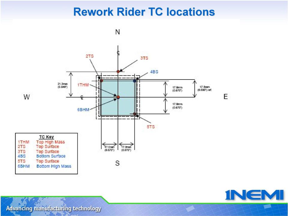
9 Rework Machine Supplier A Temperature Results Phase 1 Single Rework Machine Temperature Repeatability Results(with 99% Confidence Level in Repeatability of Temperature Measurements) TC1 Top Center Average Peak Temperature = 274ºC +/- 4ºC TC2 Top North West Component Corner = 309ºC +/- 6ºC TC3 150mils away from Component on Topside = 264ºC +/- 5ºC TC4 North East Corner on Bottomside = 318ºC +/- 5ºC TC5 Top South East Component Corner = 279ºC +/- 5ºC TC6 Bottomside Center = 272ºC +/- 5ºC 99% of the all readings are within +/-5ºC around the recorded peak temperature at each thermocouple location For example: If the recorded lead-free top component body peak temperature reading on a board was actually 250ºC, 99% of the time, the actual reading could be 5ºC lower (245ºC) or 5ºC higher (255ºC) than this value based on the temperature repeatability of this single rework machine
 or 5ºC higher")
10 Phase 1 and 2 Results (See IPC/APEX 2008 Conf. Paper) Machine Repeatability Typical Worst Case Machine A, Phase 1 +/- 5ºC TBD Machine B, Phase 1 +/- 3ºC TBD Machine C, Phase 1 +/- 7ºC TBD Machine D, Phase 1 +/- 1ºC TBD Machine A, Phase 2 +/- 6ºC TBD Machine B, Phase 2 +/- 4ºC TBD Machine C, Phase 2 +/- 6ºC TBD Machine D, Phase 2 +/- 2ºC TBD Thermocouple Repeatability +/- 1ºC +/- 2ºC Variations in temperature repeatability across rework machines of the same model from 4 different machine suppliers. Average repeatability across the four machines in the two phases to be +/- 5ºC.

11 Conclusions The repeatability tests for rework machines from four rework machine suppliers indicated an average repeatability of +/- 5ºC. The rework machine temperature profiler was found to be fairly effective in measuring temperature repeatability of the rework machine equipment. Work highlighted need to keep tighter tolerances in the form of periodic machine calibrations and temperature profiling to prevent component temperature issues during lead-free rework.

12 Future Work Phase 3 to assess the rework temperature repeatability of the same model of machine at an OEM/EMS manufacturing site. Assessments to include variations in airflow used for the rework machine/ rework nozzle heights and the effect on temperature repeatability. Other areas which may influence temperature repeatability would be preheater settings, power supply settings, nozzle design which may be considered in future testing.

13 Adjacent Component Group (Holly-Dee Rubin) INEMI Payette board: Spacing between components is 0.5 inch (13mm) Previous Findings Based on previous J-STD-020 reflow parameters To maintain peak package temperature <250 C required increased bottom heater temperatures Reworking the μbgas with increased bottom heater temperatures caused secondary reflow of the CBGA joints, and adversely impacted thermal fatigue life

14 CBGA-uBGA Interaction Study Observations: Adjacent CBGA had liquidus temperatures (0.5 inch (13mm) away) Thermal gradient across the CBGA package (see table) Joint and Package Temp Monitored Values TC Location Peak Temp (C) Reworked ubga Joint Adjacent ubga Joint CBGA 1 Joint CBGA 1 Bottom PCB CBGA 2 Joint CBGA 2 Bottom PCB CBGA 3 Joint CBGA 3 Bottom PCB Reworked CBGA CBGA Joint PCB Bottom side Heat Escape Hole CBGA CBGA solder joints below and some above liquidous temperature

15 Adjacent Component Group Objectives Stay within J-STD-020D (260 C peak) parameters when reworking components Ensure adjacent component joint temperatures remain below liquidus Solutions Explored Heat shields Rework profile reoptimization

16 Adjacent Component Temperature Results Using the increased maximum allowed package temperature in J- STD-20D, a rework profile was developed that kept the adjacent CBGA joints below the Sn3Ag0.5Cu liquidus temperature (217 C) in all cases. During rework of the U40 ubga component, the peak solder joint temperature of the CBGA (U27) was 204 C. Use of either an Aluminum or Ceramic heat shield (over the CBGA) lowered the joint temperatures on the CBGA by about 2 C to 4 C.
 was 204 C.")
17 Representative Lead-free UBGA Rework Profile (Leo Anderson, Flextronics) U40 Solder Joint peak temp.: 232 to 239 C. Time over 217C= 60 to 74 sec U40 Component top peak temp.: 255 C. Time over 217C= 109 seconds

18 Conclusions A lead-free rework profile was developed which kept the adjacent CBGA solder joints below liquidus (217 C) whilst keeping the reworked ubga component within J-STD-020D limits. Found that heat shields (Al and Ceramic) helped to reduce the temperature of the adjacent CBGA but not to a large extent (2 C to 4 C)
 helped to reduce the temperature of the")
19 Next Steps Rework more boards for cross-sectional analysis and electrical testing to confirm that the adjacent CBGA components have not undergone partial melting/reflow. Further optimize rework process ready for reworking boards for ATC testing.

20 Lead-free BGA604 Socket Rework (Alan Donaldson) Create a lead-free board rework profile for the BGA 604 socket on the INEMI Payette board Rework the sockets and verify they pass electrical test Measurement of stand-off height

21 INEMI Payette BGA604 Socket Profile Board Setup TC1-4 Socket Outer Corner Solder Joints TC5-6 Socket Center Solder Joints TC7-10 Socket Top Body TC11-12 Socket Body Top Pin Holes TC13 CAF1 Board Location
22 BGA 604 Socket Rework Temperature Profile Soak Time ( C) = 124 to 139 sec Time above liquidus (217 C) for solder joints = 137sec to 185 sec
23 BGA 604 Socket Rework Temperature Profile Thermocouple Solder Joint Description Rising Ramp Rate/ C/sec Flux Activation Time (150 C to 217 C) Critical Ramp Rate (205 C to 215 C) C/sec Socket Peak Temperature (230 C to 250 C) Socket Time Above Liquidus (40-200sec) Falling Ramp Rate/ C/sec TC1 Pin 1 Outer Corner sec C 186sec -0.2 TC2 Outer Corner sec C 180sec -0.3 TC3 Outer Corner sec C 137sec -0.2 TC4 Outer Corner sec C 159sec -0.2 TC5 Center sec C 182sec -0.1 TC6 Center sec C 185sec -0.2 Flux activation time is above target of 100 second and falling rate ramp is slow Time above liquidus (217 C) is on the high side (up to 186 sec)
24 BGA604 Socket Rework Temperature Profile (continued) Thermocouple Description Socket Body Temperature (260 C Maximum) Maximum Board Temperature TC10 Socket Top Body 257 C X TC11 Socket Top Body Pin Hole 239 C X TC13 CAF1 Board Location X 217 C Socket body below 260 C (257 C) Part of the CAF1 board area is at or above the reflow temperature (217 C) All the area within 0.7 inch of the BGA604 socket Time above liquidus for sockets are very long (up to 186 sec) because the heat gets trapped in the center The BGA rework machine had a bottom heater that is 14 X 21inch This heater size makes it hard to heat up and cool down quickly Compare this with J-STD-020D standard which indicates Time above liquidus for a component should be between 60 and 150 seconds All four reworked boards passed electrical resistance test
25 604 Socket Stand-off Results Board 22 cross-section shows that the socket sinks chips down on the A31 & AE2 corners The A31 corner stand-off is approximately 2.5mils lower The AE2 corner stand-off is approximately 3.5mils lower Board 24 cross-section shows only the AD1 corner to have a larger collapse than all other measurements The AD1 corner stand-off is approximately 4mils lower This is a fairly common observation in Lead-free BGA socket rework
26 Summary Flux activation time and falling ramp rate exceeds specification The BGA rework machine has large bottom heater which makes it hard to heat up and cool down quickly Time above liquidus for sockets are very long (up to 186sec) Compare this with J-STD-020D standard (Time above liquidus for a component should be between 60 and 150 seconds) Reworked BGA socket sinks down on the certain corners This is a fairly common observation in Lead-free BGA socket rework Reworked BGA socket passed electrical measurements
27 Next Steps Cross-sectional analysis for reworked boards for intermetallic measurements Further optimize rework process ready for reworking boards for ATC testing.
28 Previous inemi Mini-Pot Payette Board Results Showing PCB Copper Dissolution of Reworked PDIP16 Solder Joint (SnAgCu, NiAu board, 135 mil thick) Challenge Simulate current production process Remove and replace a PDIP without board preheat Dissolved copper Pad / trace Rework Observations Achieving sufficient holefill resulted in the copper pad/trace dissolution on the Cross-section View of Solder Joint (274 bottom-side Total time in mini-pot= 60sec Enough time to dissolve nickel layer
29 Mini-pot Rework (Phase 1) Generally speaking there was evidence of reduced copper dissolution when reworking 1 st pass SnAgCu wave soldered boards with Sn-Cu-Ni compared with rework using SnAgCu. Further optimization and development work will be done on the inemi Payette Board which is 125mil thick (OSP coated) with concentration on the DIMM 278 connector and DIP16 component (Phase 2)
30 PTH Rework Locations (Phase 2) 1X rework SAC305 DIP16 1X rework Sn-Cu-Ni DIP16 2X rework Sn-Cu-Ni DIP16 1X rework Sn-Cu-Ni DIMM278 2 DIMM278 Connectors 3 PDIP16 Components Note: 1 st pass wave using Sn3Ag0.5Cu
31 DIMM Connector Rework Thermocouple Locations (Phase 2) 3 Thermocouple Locations, topside lead Edge and center lead locations Monitor temperature to understand contact time required for reflow Also used to profile preheat profile Dummy copper traces on bottom side to measure copper dissolution
32 Phase 3 PTH Rework Matrix (ATC testing) PTH Rework Objectives: Validate process and reliability of reworking a Sn3Ag0.5Cu joint with Sn-Cu- Ni alloy (mixed case) Validate process and reliability (ATC) of reworking Sn3Ag0.5Cu joint with Sn3Ag0.5Cu alloy Measure levels of Cu dissolution for both types of reworked joints 1X rework on DIMM278 1X and 2X rework on DIP16
33 Next Steps Develop rework process for DIP16 with SnAgCu and SnCuNi alloys Develop rework process for DIMM278 components with SnCuNi Cross-sectional analysis for reworked boards to measure copper dissolution and solder joint integrity Further optimize rework process ready for reworking boards for ATC testing.
34 NEMI Rework Optimization Project Next Steps Group s work has concentrated on Mini-Pot rework optimization Rework Machine Temperature Repeatability Adjacent component temperatures during rework BGA socket Optimize process for Mini-pot rework, adjacent component and BGA socket rework before ATC testing of reworked boards
35 Acknowledgements The main group and sub-group chairs would like to thank the INEMI rework project team for their input and efforts into this work.
Lead Free Wave Soldering
 China - Korea - Singapore- Malaysia - USA - Netherlands - Germany WAVE SELECTIVE REFLOW SOLDERING SOLDERING SOLDERING Lead Free Wave Soldering Ursula Marquez October 18, 23 Wave Soldering Roadmap Parameter
Introduction to the Plastic Ball Grid Array (PBGA)
") Introduction to the Plastic Ball Grid Array (PBGA) Q1, 2008 Terry Burnette Dec. 15, 2005 Presentation Outline PBGA Introduction and Package Description PC Board Design for PBGA PBGA Assembly PBGA Solder
Introduction to the Plastic Ball Grid Array (PBGA) Q1, 2008 Terry Burnette Dec. 15, 2005 Presentation Outline PBGA Introduction and Package Description PC Board Design for PBGA PBGA Assembly PBGA Solder
Lead-free Wave Soldering Some Insight on How to Develop a Process that Works
 Lead-free Wave Soldering Some Insight on How to Develop a Process that Works Author: Peter Biocca, Senior Market Development Engineer, Kester, Des Plaines, Illinois. Telephone: 972.390.1197; email [email protected]
Customer Service Note Lead Frame Package User Guidelines
 Customer Service Note Lead Frame Package User Guidelines CSN30: Lead Frame Package User Guidelines Introduction Introduction When size constraints allow, the larger-pitched lead-frame-based package design
PCB inspection is more important today than ever before!
 PCB inspection is more important today than ever before! Industry experts continue to stress the need to inspect hidden solder joints! Figure 1. The BGA package has not been placed into the paste deposit.
Molded. By July. A chip scale. and Omega. Guidelines. layer on the silicon chip. of mold. aluminum or. Bottom view. Rev. 1.
 Application Note PAC-006 By J. Lu, Y. Ding, S. Liu, J. Gong, C. Yue July 2012 Molded Chip Scale Package Assembly Guidelines Introduction to Molded Chip Scale Package A chip scale package (CSP) has direct
How do you create a RoHS Compliancy-Lead-free Roadmap?
 How do you create a RoHS Compliancy-Lead-free Roadmap? When a company begins the transition to lead-free it impacts the whole organization. The cost of transition will vary and depends on the number of
Selective Soldering Defects and How to Prevent Them
 Selective Soldering Defects and How to Prevent Them Gerjan Diepstraten Vitronics Soltec BV Introduction Two major issues affecting the soldering process today are the conversion to lead-free soldering
Investigation for Use of Pin in Paste Reflow Process with Combination of Solder Preforms to Eliminate Wave Soldering
 Investigation for Use of Pin in Paste Reflow Process with Combination of Solder Preforms to Eliminate Wave Soldering Guhan Subbarayan, Scott Priore Assembly Sciences and Technology, Cisco Systems, Inc.
Assembly of LPCC Packages AN-0001
 Assembly of LPCC Packages AN-0001 Surface Mount Assembly and Handling of ANADIGICS LPCC Packages 1.0 Overview ANADIGICS power amplifiers are typically packaged in a Leadless Plastic Chip Carrier (LPCC)
How To Clean A Copper Board With A Socket On It (Ios)
") Den-on Rework Reference Process for Desktop platform and new Intel Socket LGA-1156 using the Den-on BGA rework station RD-500II and III *This document shows the whole process on how to repair the Intel
Den-on Rework Reference Process for Desktop platform and new Intel Socket LGA-1156 using the Den-on BGA rework station RD-500II and III *This document shows the whole process on how to repair the Intel
Technical Note Recommended Soldering Parameters
 Technical Note Recommended Soldering Parameters Introduction Introduction The semiconductor industry is moving toward the elimination of Pb from packages in accordance with new international regulations.
Taking the Pain Out of Pb-free Reflow
 Taking the Pain Out of Pb-free Reflow Paul N. Houston & Brian J. Lewis Siemens Dematic Electronics Assembly Systems (770) 797-3362 Presented at APEX 2003, Anaheim CA Daniel F. Baldwin Engent, Inc. Norcross,
Bob Willis leadfreesoldering.com
 Assembly of Flexible Circuits with Lead-Free Solder Alloy Bob Willis leadfreesoldering.com Introduction to Lead-Free Assembly Video Clips Component www.bobwillis.co.uk/lead/videos/components.rm Printed
RE-8500 BGA Rework Station
 Jovy Systems Limited RE-8500 BGA Rework Station User Manual Ver1.0 1 Contents 1- Introduction. Page:4 a. General product information b. RE-8500 features c. Field of applications and components types d.
Wurth Electronics Midcom Policy Statement on RoHS Compliance And Lead-Free Products
 Wurth Electronics Midcom Policy Statement on RoHS Compliance And Lead-Free Products General Environmental Policy Wurth Electronics Midcom is committed to the manufacture of environmentally-friendly products
Edition 2012-032 Published by Infineon Technologies AG 81726 Munich, Germany 2013 Infineon Technologies AG All Rights Reserved.
 Recommendations for Printed Circuit Board Assembly of Infineon Laminate Packages Additional Information DS1 2012-03 Edition 2012-032 Published by Infineon Technologies AG 81726 Munich, Germany 2013 Infineon
Lead-Free Wave Soldering of High Complexity PWB s
 Lead-Free Wave Soldering of High Complexity PWB s The transition to lead-free wave soldering has brought with it many challenges. As with any new manufacturing technology entering a production environment,
PRODUCT PROFILE. ELECTROLOY in partnership with FCT Asia Pte Limited. in manufacturing. Nihon Superior Lead Free Solder Bar.
 PRODUCT PROFILE ELECTROLOY in partnership with FCT Asia Pte Limited in manufacturing Nihon Superior Lead Free Solder Bar SN100C Product Name Product Code LEAD FREE BAR LEAD FREE BAR ( TOP UP ALLOY ) SN100C
BGA - Ball Grid Array Inspection Workshop. Bob Willis leadfreesoldering.com
 BGA - Ball Grid Array Inspection Workshop Bob Willis leadfreesoldering.com Mixed Technology Assembly Processes Adhesive Dispensing Component Placement Adhesive Curing Turn Boar Over Conventional Insertion
Application Note AN-0994 Maximizing the Effectiveness of your SMD Assemblies
 Application Note AN-0994 Maximizing the Effectiveness of your SMD Assemblies Table of Contents Page Method...2 Thermal characteristics of SMDs...2 Adhesives...4 Solder pastes...4 Reflow profiles...4 Rework...6
Rework stations: Meeting the challenges of lead-free solders
 Rework stations: Meeting the challenges of lead-free solders Market forces, particularly legislation against the use of lead in electronics, have driven electronics manufacturers towards lead-free solders
REVISION HISTORY APPROVERS
 REVISION HISTORY Revision Description of Change Writer/Reviser Effective Date 1.0 As Issued. Renumbered from PEC-MAT-2-003-00. Lenora Bennett January 23, 2012 2.0 Updated Table 1 Nickel barrier specifications
Flip Chip Package Qualification of RF-IC Packages
 Flip Chip Package Qualification of RF-IC Packages Mumtaz Y. Bora Peregrine Semiconductor San Diego, Ca. 92121 [email protected] Abstract Quad Flat Pack No Leads (QFNs) are thermally enhanced plastic packages
AND8464/D. Board Level Application Note for 0402, 0502 and 0603 DSN2 Packages APPLICATION NOTE
 Board Level Application Note for 0402, 0502 and 0603 DSN2 Packages Prepared by: Denise Thienpont, Steve St. Germain ON Semiconductor APPLICATION NOTE Introduction ON Semiconductor has introduced an expanded
Component Candidacy of Second Side Reflow with Lead-Free Solder
 Materials Transactions, Vol. 47, No. 6 (006) pp. 577 to 583 #006 The Japan Institute of Metals Component Candidacy of Second Side Reflow with Lead-Free Solder Yueli Liu ; *, David A. Geiger and Dongkai
Ceramic Ball Grid Array Packaging, Assembly & Reliability. Freescale Semiconductor
 Ceramic Ball Grid Array Packaging, Assembly & Reliability 1 Outline for Discussion Why BGA???? CBGA Introduction and Package Description PC Board Design for CBGA CBGA Assembly Rework Board-Level Solder
Printed Circuit Design Tutorial
 Printed Circuit Design Tutorial By Gold Phoenix Technology Tech Center, [email protected] Gold Phoenix has been sale PCB board in North America since 2003, during these years we received a lot of
17 IMPLEMENTATION OF LEAD-FREE SOLDERING TECHNOLOGY. Eva Kotrčová České Vysoké Učení Technické Fakulta Elektrotechnická Katedra Elektrotechnologie
 17 IMPLEMENTATION OF LEAD-FREE SOLDERING TECHNOLOGY Eva Kotrčová České Vysoké Učení Technické Fakulta Elektrotechnická Katedra Elektrotechnologie 1. Introduction Lead is the toxic heavy metal which is
Solder Reflow Guide for Surface Mount Devices
 June 2015 Introduction Technical Note TN1076 This technical note provides general guidelines for a solder reflow and rework process for Lattice surface mount products. The data used in this document is
Lead Free Reliability Testing
 Lead Free Reliability Testing Reliability Implications of Lead-Free Reliability, of what? Solder Joints Laminate Solder Joint Reliability Components SAC vs. SAC main alternative alloy Comparison is desired,
PCB Assembly Guidelines for Intersil Wafer Level Chip Scale Package Devices
 Assembly Guidelines for Intersil Wafer Level Chip Scale Package Devices Introduction There is an industry-wide trend towards using the smallest package possible for a given pin count. This is driven primarily
Lead-Free Product Transition: Impact on Printed Circuit Board Design and Material Selection
 Presented in the ECWC 10 Conference at IPC Printed Circuits Expo, SMEMA Council AP EX and Designers Summit 05 Lead-Free Product Transition: Impact on Printed Circuit Board Design and Material Selection
RoHS-Compliant Through-Hole VI Chip Soldering Recommendations
 APPLICATION NOTE AN:017 RoHS-Compliant Through-Hole VI Chip Soldering Recommendations Ankur Patel Associate Product Line Engineer Contents Page Introduction 1 Wave Soldering 1 Hand Soldering 4 Pin/Lead
TN0991 Technical note
 Technical note Description of WLCSP for STMicroelectronics EEPROMs and recommendations for use Introduction This document describes the 5 and 8-bump WLCSPs (wafer level chip size package) used for STMicroelectronics
How to avoid Layout and Assembly got chas with advanced packages
 How to avoid Layout and Assembly got chas with advanced packages Parts and pitch get smaller. Pin counts get larger. Design cycles get shorter. BGA, MicroBGA, QFN, DQFN, CSP packages are taking the design
Good Boards = Results
 Section 2: Printed Circuit Board Fabrication & Solderability Good Boards = Results Board fabrication is one aspect of the electronics production industry that SMT assembly engineers often know little about.
PRINTED CIRCUIT BOARD SURFACE FINISHES - ADVANTAGES AND DISADVANTAGES
 PRINTED CIRCUIT BOARD SURFACE FINISHES - ADVANTAGES AND DISADVANTAGES By Al Wright, PCB Field Applications Engineer Epec Engineered Technologies Anyone involved within the printed circuit board (PCB) industry
Solutions without Boundaries. PCB Surface Finishes. Todd Henninger, C.I.D. Sr. Field Applications Engineer Midwest Region
 Solutions without Boundaries PCB Surface Finishes Todd Henninger, C.I.D. Sr. Field Applications Engineer Midwest Region 1 Notice Notification of Proprietary Information: This document contains proprietary
User Guide Reflow Toaster Oven Controller
 User Guide Reflow Toaster Oven Controller Version 1.5-01/10/12 DROTEK Web shop: www.drotek.fr SOMMAIRE 1. Introduction... 3 2. Preparation of THE REFLOW CONTROLLER... 4 2.1. Power supply... 4 2.2. USB
Handling and Processing Details for Ceramic LEDs Application Note
 Handling and Processing Details for Ceramic LEDs Application Note Abstract This application note provides information about the recommended handling and processing of ceramic LEDs from OSRAM Opto Semiconductors.
touchbga.com TOUCHBGA BGA Rework Station IR-PRO-SC v6 User Manual
 TOUCHBGA BGA Rework Station IR-PRO-SC v6 User Manual Table of contents 1. IR-PRO-SC v6 BGA rework station features 1.1.Safety Instrouctions 1.1.1.Electric Safety 1.1.1.Operation Safety 1.1.3.Environmental
Lead-free Defects in Reflow Soldering
 Lead-free Defects in Reflow Soldering Author: Peter Biocca, Senior Development Engineer, Kester, Des Plaines, Illinois. Telephone 972.390.1197; email [email protected] February 15 th, 2005 Lead-free Defects
SOLDER CHARGE SMT: THE DESIGN AND VALIDATION OF NEW SOLDER ATTACH TECHNOLOGIES
 SOLDER CHARGE SMT: THE DESIGN AND VALIDATION OF NEW SOLDER ATTACH TECHNOLOGIES Jim Hines 1, Kirk Peloza 2, Adam Stanczak 3, David Geiger 4 1 Molex Lisle, IL, USA 2 Molex Lisle, IL, USA 3 Molex Lisle, IL,
MS9000SAN Rework Station
 MS9000SAN Rework Station MS9000SAN is the all-round rework system which almost all SMD can be reworked. And the original ITTS auto profiler system is operates of the system easily and exactly. Many kinds,
A and M Electronics Contract Manufacturing Circuit Board Assembly 25018 Avenue Kearny Valencia, Ca. 91355 (661) 257-3680 or (800) 923-3058
 257-3680 or (800) 923-3058") A and M Electronics Contract Manufacturing Circuit Board Assembly 25018 Avenue Kearny Valencia, Ca. 91355 (661) 257-3680 or (800) 923-3058 "When Quality Counts, Choose A&M Electronics" SMT, BGA, & Through
A and M Electronics Contract Manufacturing Circuit Board Assembly 25018 Avenue Kearny Valencia, Ca. 91355 (661) 257-3680 or (800) 923-3058 "When Quality Counts, Choose A&M Electronics" SMT, BGA, & Through
Soldering Methods and Procedures for Vicor Power Modules
 APPLICATION NOTE Soldering Methods and Procedures for Vicor Power Modules LEAD-FREE PINS (ROHS); TIN / LEAD PINS see page 6 OVERVIEW The following pages contain soldering information for the following
CONSIDERATIONS FOR SELECTING A PRINTED CIRCUIT BOARD SURFACE FINISH
 CONSIDERATIONS FOR SELECTING A PRINTED CIRCUIT BOARD SURFACE FINISH Randy Schueller, Ph.D. DfR Solutions Minneapolis, MN, USA [email protected] ABSTRACT The selection of the surface finish to
Product Specification
 Product Specification Model No.: DC-240-L01-00-TR Description: H=3.00mm Horizontal SMD DC Power Jacks Pin Shaft Diameter: 0.65mm Packing Method: Tape & Reel (600pcs./R) 1. General 1a. Scope The jacks should
Application Note. Soldering Methods and Procedures for 1st and 2nd Generation Power Modules. Overview. Analysis of a Good Solder Joint
 Soldering Methods and Procedures for 1st and 2nd Generation Power Modules Overview This document is intended to provide guidance in utilizing soldering practices to make high quality connections of Vicor
ENIG with Ductile Electroless Nickel for Flex Circuit Applications
 ENIG with Ductile Electroless Nickel for Flex Circuit Applications Yukinori Oda, Tsuyoshi Maeda, Chika Kawai, Masayuki Kiso, Shigeo Hashimoto C.Uyemura & Co., Ltd. George Milad and Donald Gudeczauskas
Designing with High-Density BGA Packages for Altera Devices
 2014.12.15 Designing with High-Density BGA Packages for Altera Devices AN-114 Subscribe As programmable logic devices (PLDs) increase in density and I/O pins, the demand for small packages and diverse
Auditing Contract Manufacturing Processes
 Auditing Contract Manufacturing Processes Greg Caswell and Cheryl Tulkoff Introduction DfR has investigated multiple situations where an OEM is experiencing quality issues. In some cases, the problem occurs
Compliant Terminal Technology Summary Test Report
 Engineering Report ER04100 October 5th, 2004 Revision A Copyright Autosplice Inc., September 2004 Table of Contents Summary Overview 3 Compliant Terminal Specifications 3 Test Plan 4 Test Conditions 4
Electronic Board Assembly
 Electronic Board Assembly ERNI Systems Technology Systems Solutions - a one stop shop - www.erni.com Contents ERNI Systems Technology Soldering Technologies SMT soldering THR soldering THT soldering -
ALPHA OL-107F-A ZERO-HALOGEN, LOW VOIDS, FINE FEATURE, EXCELLENT PIN TEST PERFORMANCE, NO-CLEAN, LEAD-FREE SOLDER PASTE
 T E C H N I C A L B U L L E T I N ALPHA OL-107F-A ZERO-HALOGEN, LOW VOIDS, FINE FEATURE, EXCELLENT PIN TEST PERFORMANCE, NO-CLEAN, LEAD-FREE SOLDER PASTE DESCRIPTION ALPHA OL-107F-A is a lead-free, Zero-halogen
Mounting Instructions for SP4 Power Modules
 Mounting Instructions for SP4 Power Modules Pierre-Laurent Doumergue R&D Engineer Microsemi Power Module Products 26 rue de Campilleau 33 520 Bruges, France Introduction: This application note gives the
DSP 215D (Sn/Ag/Cu) LEAD FREE RMA DISPENSING SOLDER PASTE
 LEAD FREE RMA DISPENSING SOLDER PASTE") SN/AG/CU. 862 Rev.A TECHNICAL DATA SHEET TECHNICAL SPECIFICATIONS SN/AG/CU. 862 Rev DSP 215D (Sn/Ag/Cu) LEAD FREE RMA DISPENSING SOLDER PASTE CORPORATE HEADQUARTERS USA: 315 Fairbank St. Addison, IL 60101!
SN/AG/CU. 862 Rev.A TECHNICAL DATA SHEET TECHNICAL SPECIFICATIONS SN/AG/CU. 862 Rev DSP 215D (Sn/Ag/Cu) LEAD FREE RMA DISPENSING SOLDER PASTE CORPORATE HEADQUARTERS USA: 315 Fairbank St. Addison, IL 60101!
Overview of Rigid Flex Technology. Joseph Fjelstad
 Overview of Rigid Flex Technology Joseph Fjelstad Background Flexible circuits have seen explosive growth in recent times owing to their numerous advantages as an interconnection medium. Presently nearly
HSD High Speed Data interconnection
 HSD High Speed Data interconnection Fast, safe and robust Very high data bit rate up to 5 Gbit/s SSR smart strain relief enables unstressed solder joints Excellent resistance against cross-talk and RF-EMC
MuAnalysis. Printed Circuit Board Reliability and Integrity Characterization Using MAJIC. M. Simard-Normandin MuAnalysis Inc. Ottawa, ON, Canada
 Printed Circuit Board Reliability and Integrity Characterization Using MAJIC M. Simard-Normandin Inc. Ottawa, ON, Canada Abstract The recent need to develop lead-free electrical and electronic products
What is surface mount?
 A way of attaching electronic components to a printed circuit board The solder joint forms the mechanical and electrical connection What is surface mount? Bonding of the solder joint is to the surface
For board-to-fpc. Narrow Pitch Connectors (0.35mm pitch)
") For board-to-fpc Narrow Pitch Connectors (0.35mm pitch) S35 Series New FEATURES 1. 1.7 mm wide slim two-piece type connector Mated height 0.6 mm Smaller compared to A4F series Width: Approx. 44% down
For board-to-fpc Narrow Pitch Connectors (0.35mm pitch) S35 Series New FEATURES 1. 1.7 mm wide slim two-piece type connector Mated height 0.6 mm Smaller compared to A4F series Width: Approx. 44% down
Edition 2012-05 Published by Infineon Technologies AG 81726 Munich, Germany 2012 Infineon Technologies AG All Rights Reserved.
 Recommendations for Printed Circuit Board Assembly of Infineon QFN Packages Additional Information DS7, 2012-05 Edition 2012-05 Published by Infineon Technologies AG 81726 Munich, Germany 2012 Infineon
Small Form- Factor Pluggable (SFP) DWDM
 DWDM") Small Form- Factor Pluggable (SFP) DWDM Application Specification (Dense Wavelength Division Multiplexer) 114-13178 Connector and Cage Assembly 02 MAY 11 Rev F NOTE i All numerical values are in metric
Small Form- Factor Pluggable (SFP) DWDM Application Specification (Dense Wavelength Division Multiplexer) 114-13178 Connector and Cage Assembly 02 MAY 11 Rev F NOTE i All numerical values are in metric
Printed Circuit Boards
 Printed Circuit Boards Luciano Ruggiero [email protected] DEIS Università di Bologna Flusso di progetto di un circuito stampato 1 Specifications Before starting any design, you need to work out the
Wave Soldering Problems
 Wave Soldering Problems What is a good joint? The main function of the solder is to make electrical interconnection, but there is a mechanical aspect: even where parts have been clinched or glued in position,
White Paper. Recommendations for Installing Flash LEDs on Flex Circuits. By Shereen Lim. Abstract. What is a Flex Circuit?
 Recommendations for Installing Flash LEDs on Circuits By Shereen Lim White Paper Abstract For the mobile market some PCB assemblies have been converted to flex circuit assemblies, in part because flex
Wafer Level Chip Scale Package (WLCSP)
") Freescale Semiconductor Application Note AN3846 Rev. 3.0, 05/2012 Wafer Level Chip Scale Package (WLCSP) 1 Purpose This document provides guidelines to use the Wafer Level Chip Scale Package (WLCSP) to
Freescale Semiconductor Application Note AN3846 Rev. 3.0, 05/2012 Wafer Level Chip Scale Package (WLCSP) 1 Purpose This document provides guidelines to use the Wafer Level Chip Scale Package (WLCSP) to
Ball Grid Array (BGA) Technology
 Technology") Chapter E: BGA Ball Grid Array (BGA) Technology The information presented in this chapter has been collected from a number of sources describing BGA activities, both nationally at IVF and reported elsewhere
Chapter E: BGA Ball Grid Array (BGA) Technology The information presented in this chapter has been collected from a number of sources describing BGA activities, both nationally at IVF and reported elsewhere
Flux gel is available in 10 and 30 cc syringes for rework applications Complies with RoHS Directive 2002/95/EC
 DESCRIPTION ALPHA CVP-390 is a lead-free, Zero-halogen no-clean solder paste designed for applications where residue with excellent pin testing property and ability to pass JIS Copper Corrosion test are
Report. Soldering Tests at COM Express Connectors, Type Receptacle and Plug. Order: Bergwerkstraße 50 D 86971 Peiting. Your Order-No.
 Zentrum für Verbindungstechnik in der Elektronik Argelsrieder Feld 6 82234 Oberpfaffenhofen-Weßling Telefon: 081 53 / 403-0 Telefax: 081 53 / 403-15 Report Order: Soldering Tests at COM Express Connectors,
HOT BAR REFLOW SOLDERING FUNDAMENTALS. A high quality Selective Soldering Technology
 HOT BAR REFLOW SOLDERING FUNDAMENTALS A high quality Selective Soldering Technology Content 1. Hot Bar Reflow Soldering Introduction 2. Application Range 3. Process Descriptions > Flex to PCB > Wire to
Overview of Risk Assessment, Mitigation, and Management Research for Pb-free Electronics
 Overview of Risk Assessment, Mitigation, and Management Research for Pb-free Electronics Formed 1987 Electronic Products and Systems Center College Park, MD 20742 (301) 405-5323 http://www.calce.umd.edu
Multilevel Socket Technologies
 Multilevel Socket Technologies High Performance IC Sockets And Test Adapters Overview Company Overview Over 5,000 products High Performance Adapters and Sockets Many Custom Designs & Turn-Key Solutions
WCAP-CSGP Ceramic Capacitors
 A Dimensions: [mm] B Recommended land pattern: [mm] D1 Electrical Properties: Properties Test conditions Value Unit Tol. Capacitance 1±0.2 Vrms, 1 khz ±10% C 15000 pf ± 10% Rated voltage Dissipation factor
Lead-free Hand-soldering Ending the Nightmares
 Lead-free Hand-soldering Ending the Nightmares Most issues during the transition seem to be with Hand-soldering As companies transition over to lead-free assembly a certain amount of hand-soldering will
1 POLE 5 A (CADMIUM FREE CONTACTS TYPE) NY SERIES
 NY SERIES") POWER RELAY 1 POLE 5 A (CADMIUM FREE CONTACTS TYPE) NY SERIES RoHS compliant FEATURES Ultra slim type with 5 mm thickness Good for high density mounting Low power consumption and high sensitivity Nominal
POWER RELAY 1 POLE 5 A (CADMIUM FREE CONTACTS TYPE) NY SERIES RoHS compliant FEATURES Ultra slim type with 5 mm thickness Good for high density mounting Low power consumption and high sensitivity Nominal
Crack Detection Methods For Lead-free Solder Joints
 NPL Report MATC(A)164 Crack Detection Methods For Lead-free Solder Joints Milos Dusek & Christopher Hunt March 2004 Crack Detection Methods for Lead-free Solder Joints Miloš Dušek and Christopher Hunt
ALPHA CVP-390 - NO-CLEAN, LEAD-FREE SOLDER PASTE ZERO-HALOGEN, LOW VOIDS, FINE FEATURE, EXCELLENT PIN TEST PERFORMANCE, SAC305 AND LOW AG CAPABLE.
 T E C H N I C A L B U L L E T I N ALPHA CVP-390 - NO-CLEAN, LEAD-FREE SOLDER PASTE ZERO-HALOGEN, LOW VOIDS, FINE FEATURE, EXCELLENT PIN TEST PERFORMANCE, SAC305 AND LOW AG CAPABLE. DESCRIPTION ALPHA CVP-390
Application Note AN-1170. Audio Power Quad Flat No-Lead (PQFN) Board Mounting Application Note
 Board Mounting Application Note") Application Note AN-1170 Audio Power Quad Flat No-Lead (PQFN) Board Mounting Application Note Table of Contents Page Device construction...2 Design considerations...3 Assembly considerations...4 Mechanical
Application Note AN-1170 Audio Power Quad Flat No-Lead (PQFN) Board Mounting Application Note Table of Contents Page Device construction...2 Design considerations...3 Assembly considerations...4 Mechanical
DETECTION OF DEFECT ON FBGA SOLDER BALLS USING X-RAY TECHNOLOGY
 DETECTION OF DEFECT ON FBGA SOLDER BALLS USING X-RAY TECHNOLOGY Pavel Řihák Doctoral Degree Programme (2), FEEC BUT E-mail: [email protected] Supervised by: Ivan Szendiuch E-mail: [email protected]
RJR Polymers Reliability Qualification Report RQFN55-24-A and RQFN44-12-A
 Reliability Qualification Report RQFN55-24-A and RQFN44-12-A Package Qualification September 14, 2011 RJR Polymers Reliability Qualification Report RQFN55-24-A and RQFN44-12-A Table of Contents Purpose.3
Thermal Management Solutions for Printed Circuit Boards used in Digital and RF Power Electronics and LED assemblies
 Thermal Management Solutions for Printed Circuit Boards used in Digital and RF Power Electronics and LED assemblies Sandy Kumar, Ph.D. Director of Technology American Standard Circuits, Inc 3615 Wolf Road
How to Build a Printed Circuit Board. Advanced Circuits Inc 2004
 How to Build a Printed Circuit Board 1 This presentation is a work in progress. As methods and processes change it will be updated accordingly. It is intended only as an introduction to the production
, Yong-Min Kwon 1 ) , Ho-Young Son 1 ) , Jeong-Tak Moon 2 ) Byung-Wook Jeong 2 ) , Kyung-In Kang 2 )
 , Ho-Young Son 1 ) , Jeong-Tak Moon 2 ) Byung-Wook Jeong 2 ) , Kyung-In Kang 2 )") Effect of Sb Addition in Sn-Ag-Cu Solder Balls on the Drop Test Reliability of BGA Packages with Electroless Nickel Immersion Gold (ENIG) Surface Finish Yong-Sung Park 1 ), Yong-Min Kwon 1 ), Ho-Young
Effect of Sb Addition in Sn-Ag-Cu Solder Balls on the Drop Test Reliability of BGA Packages with Electroless Nickel Immersion Gold (ENIG) Surface Finish Yong-Sung Park 1 ), Yong-Min Kwon 1 ), Ho-Young
Accelerometer and Gyroscope Design Guidelines
 Application Note Accelerometer and Gyroscope Design Guidelines PURPOSE AND SCOPE This document provides high-level placement and layout guidelines for InvenSense MotionTracking devices. Every sensor has
Quad Flat Package (QFP)
") Freescale Semiconductor Application Note AN4388 Rev. 2.0, 2/2014 Quad Flat Package (QFP) 1 Introduction This document provides guidelines for handling and assembly of Freescale QFP packages during Printed
Freescale Semiconductor Application Note AN4388 Rev. 2.0, 2/2014 Quad Flat Package (QFP) 1 Introduction This document provides guidelines for handling and assembly of Freescale QFP packages during Printed
LDO03C/LDO06C/LDO10C
 NEW LDO03C/LDO06C/LDO10C A p p l i c a t i o n N o t e 1 8 6 1. Introduction 2 2. Models Features 2 3. General Description Electrical Description 2 Physical Construction 2 4. Features and Functions Wide
Reballing Rework Bright New Future
 Reballing Rework Bright New Future Components are continuing to evolve. One of those evolutions is the Ball Grid Array or BGA. Add in the advent of the RoHS and WEEE directives and rework of the BGA is
Today's Vapor Phase Soldering An Optimized Reflow Technology for Lead Free Soldering
 Today's Vapor Phase Soldering An Optimized Reflow Technology for Lead Free Soldering Dipl.-Ing. Helmut Leicht; Andreas Thumm IBL-Löttechnik GmbH www.ibl-loettechnik.de, Germany ABSTRACT In the beginning
Evaluation of Soft Soldering on Aluminium Nitride (AlN) ESTEC Contract No. 19220/05/NL/PA. CTB Hybrids WG ESTEC-22nd May 2007
 ESTEC Contract No. 19220/05/NL/PA. CTB Hybrids WG ESTEC-22nd May 2007") Evaluation of Soft Soldering on Aluminium Nitride (AlN) ESTEC Contract No. 19220/05/NL/PA CTB Hybrids WG ESTEC-22nd May 2007 Evaluation of Soft Soldering on AlN Schedule Project presentation Feasibility
Evaluation of Soft Soldering on Aluminium Nitride (AlN) ESTEC Contract No. 19220/05/NL/PA CTB Hybrids WG ESTEC-22nd May 2007 Evaluation of Soft Soldering on AlN Schedule Project presentation Feasibility
Metal-Oxide Varistors (MOVs) Surface Mount Multilayer Varistors (MLVs) > MLN Series. MLN SurgeArray TM Suppressor. Description
 Surface Mount Multilayer Varistors (MLVs) > MLN Series. MLN SurgeArray TM Suppressor. Description") MLN SurgeArray TM Suppressor RoHS Description The MLN SurgeArray Suppressor is designed to help protect components from transient voltages that exist at the circuit board level. This device provides four
MLN SurgeArray TM Suppressor RoHS Description The MLN SurgeArray Suppressor is designed to help protect components from transient voltages that exist at the circuit board level. This device provides four
Comparative Wetting Ability of Lead-Free Alloys
 Comparative Wetting Ability of Lead-Free Alloys Understanding the wetting kinetics of lead-free alloys becomes crucial in selecting a suitable lead-free composition for assembling PCBs. KaiHwa Chew, Vincent
LEAD FREE HALOGENFREE. Würth Elektronik PCB Design Conference 2007. Lothar Weitzel 2007 Seite 1
 LEAD FREE HALOGENFREE Würth Elektronik PCB Design Conference 2007 Lothar Weitzel 2007 Seite 1 Content Solder surfaces/overview Lead free soldering process requirements/material parameters Different base
Difference Between Various Sn/Ag/Cu Solder Compositions. Almit Ltd. Tadashi Sawamura Takeo Igarashi
 Difference Between Various Sn/Ag/Cu Solder Compositions Almit Ltd. Tadashi Sawamura Takeo Igarashi 29/6/2005 Table Of Contents 1. Overview 2. Mechanical Properties 3. Reliability Results 4. Conclusion
How To Test A Sidactor Series For A Power Supply
 SDP Series - SOT23-5 RoHS Pb e3 Description This new SIDACtor series is targeted for the tertiary or line driver side protection position for VDSL2+, ADSL2 applications and general I/O protection functions.
Q&A. Contract Manufacturing Q&A. Q&A for those involved in Contract Manufacturing using Nelco Electronic Materials
 Q&A Q&A for those involved in Contract Manufacturing using Nelco Electronic Materials 1. Do Nelco laminates have any discoloration effects or staining issues after multiple high temperature exposures?