Cross-Interaction Between Au and Cu in Au/Sn/Cu Ternary Diffusion Couples
|
|
|
- Alexandrina Carson
- 9 years ago
- Views:
Transcription
1 Cross-Interaction Between Au and Cu in Au/Sn/Cu Ternary Diffusion Couples C. W. Chang 1, Q. P. Lee 1, C. E. Ho 1 1, 2, *, and C. R. Kao 1 Department of Chemical & Materials Engineering 2 Institute of Materials Science & Engineering National Central University Jhongli City, Taiwan (* [email protected] Phone/Fax: ) Both Au and Cu are so-called fast diffusers in Sn, and can diffuse very long distances in Sn in a relatively short time. In this study, the cross-interaction between Au and Cu across a layer of Sn was investigated through the use of the Au/Sn/Cu ternary diffusion couples. A seven µm Au layer and a 100 µm Sn layer were electroplated over Cu foils to produce the Au/Sn/Cu diffusion couples. Aging at 200 o C revealed that cross-interaction could occur in as short as 10 minutes. Evidence of this cross-interaction included the formation of (Cu 1-x Au x ) 6 Sn 5 on the Au side of the diffusion couples as well as on the Cu side. The reaction products on the Au side included the Au-Sn binary compounds. Between the Au-Sn compounds and the Sn was (Cu 1-x Au x ) 6 Sn 5. The reaction products on the Cu side initially was only (Cu 1-x Au x ) 6 Sn 5, but a layer of Au-free Cu 3 Sn eventually formed between (Cu 1-x Au x ) 6 Sn 5 and Cu. A detailed atomic flux analysis showed that the Cu flux through the Sn layer was about 2-3 times higher than the Au flux at any moment. The results of this study show that the cross-interaction of Au and Cu in solders is extremely rapid, and cannot be ignored in those solder joints that have both elements present. Keywords: Au-Sn-Cu, cross-interaction, lead-free solder. 1

2 1. Introduction In electronic packages, the surface of the soldering pads is often coated with an Au layer to provide oxidation protection. This Au layer will rapidly dissolve into solder during reflow and form AuSn 4 particles dispersed inside the solder joint after reflow [1-3]. These AuSn 4 particles, when present in a large amount, are known to cause reliability problems, such as the brittle fracture of a solder joint [4-12]. The element Cu is also an element which is often in direct contact with the solders because it is the most common metal used as the conducting lines on the Si devices, substrates, and printed circuit boards. In fact, Cu is one of the constituents in the Sn-Ag-Cu lead-free solder family. Both Au and Cu are very mobile in solders, and can diffuse across very long distances in a relatively short time. Consequently, Cu and Au might interact even if they are separated by a thick layer of solder. The objective of this study is to investigate the cross-interaction between Au and Cu across a layer of Sn. In other words, we will study the Au/Sn/Cu ternary diffusion couple. A literature search revealed that there was no such study reported. Nevertheless, there are preliminary evidences showing that Au and Cu do interact in solders [13, 14]. The Au/Sn/Cu diffusion couple is a rather ideal system for studying such type of cross-interaction. This is because both the Au/Sn and Sn/Cu binary reactions have been well studied. In addition, the AuCuSn ternary isotherm is also well characterized. For a summary of the Au/Sn and Sn/Cu binary reactions, see a book chapter written by Zakel and Reichl [15]. The AuCuSn ternary isotherm at 190 o C, determined by Zakel [16], is reproduced in Fig. 1. The Au/Sn/Cu ternary diffusion couples used in this study were prepared by sequentially electroplating a layer of Sn and a layer of Au over the Cu substrate. There are two benefits by using such a method to prepare the diffusion couples. The first is that the distance between Au and Cu (or the Sn thickness) can be controlled at will. The second is 2
![These AuSn 4 particles, when present in a large amount, are known to cause reliability problems, such as the brittle fracture of a solder joint [4-12].](/docs-images/46/21268357/images/page_2.jpg "The element Cu is also an element which is often in direct contact with the solders because it is the most common metal used as the conducting lines on the Si devices, substrates, and printed circuit")
3 that the diffusion couples will not experience any high temperature processing step before the diffusion couples are subjected to the planned interdiffusion. If the diffusion couple had been prepared by melting the solder to bond Au and Cu, then a certain degree of cross-interaction might have occurred during bonding. The cross-interaction during the bonding stage could be, in fact, substantial because it had been reported that Cu and Ni could cross-interact during the reflow [17]. Consequently, in those diffusion couples bonded by melting, it will be difficult to distinguish to the extent of the cross-interactions that have occurred during the bonding stage from that during the reaction stage. 2. Experimental The Au/Sn/Cu diffusion couples were prepared by electroplating a seven µm Au layer and a 100 µm Sn layer over the Cu foil substrate. The Cu foil was 400 µm thickness and 99.6 wt% pure. Before electroplating, each Cu foil surface was polished, with one µm diamond abrasive used in the last polishing step. The Cu foil was then lightly etched in a 5 vol% HNO 3 -CH 3 OH solution for one minute, and cleaned with deionized water. After electroplating the Au and Sn layers, the foil was cut into 4 mm 8 mm diffusion couples. The diffusion couples were then subjected to aging at 200 o C. After aging, these samples were mounted in epoxy, sectioned by using a low-speed diamond saw, and metallographically polished to reveal the microstructure. The reaction zone for each diffusion couple was examined by using the optical microscopy (OM) and the scanning electron microscopy (SEM). The compositions of the intermetallic compounds were determined by the electron probe micro-analysis (EPMA). In EPMA analysis, the concentration of each element was measured independently, and the total weight percentage 3
![The cross-interaction during the bonding stage could be, in fact, substantial because it had been reported that Cu and Ni could cross-interact during the reflow [17].](/docs-images/46/21268357/images/page_3.jpg "Consequently, in those diffusion couples bonded by melting, it will be difficult to distinguish to the extent of the cross-interactions that have occurred during the bonding stage from that during")
4 of all elements was within 100 ± 1% in each case. The average value from at least three measurements was then reported. 3. Results The as-deposited Au/Sn/Cu diffusion couple is shown in Fig. 1. As can be seen here, there was no evidence of interfacial reaction during the electroplating of Au and Sn. Nevertheless, the interfacial reaction occurred very quickly at 200 o C, as shown in Fig. 2 for a diffusion couple that had been aged for 10 minutes. Figure 2 (a) shows that three Au-Sn binary compounds, AuSn, AuSn 2, and AuSn 4, and an Au-Cu-Sn ternary compound existed at the original Au/Sn interface. Basing on the results that are to be presented later, we propose this Au-Cu-Sn compound has the Cu 6 Sn 5 crystal structure with a small amount of Au dissolved in the Cu sublattice, i.e. (Cu 1-x Au x ) 6 Sn 5. The fast Au-Sn reaction is not surprising, as such rapid reaction had been reported before [15, 18]. However, the formation of (Cu 1-x Au x ) 6 Sn 5 after only 10 minutes of aging is unexpected. As the only source of Cu was from the opposite side of the diffusion couple, the formation of (Cu 1-x Au x ) 6 Sn 5 on the Au side suggested that the cross-interaction between the Au/Sn and the Sn/Cu interface had occurred across a 100 µm layer of Sn in 10 minutes. The original Sn/Cu interface also shows evidence of this cross-interaction. We had detected strong Au signal that could not attributed to background noise from the Cu 6 Sn 5 phase between Sn and Cu in Fig. 2(c). In other words, Au atoms had diffused through the Sn layer to be incorporated into Cu 6 Sn 5. It should be stressed again that during the sample preparation step, Sn did not go through the molten state. The results above were purely from a solid-state interdiffusion at 200 o C. The cross-interaction proceeded even further when the aging time reached 400 minutes, 4
 6 Sn 5.")
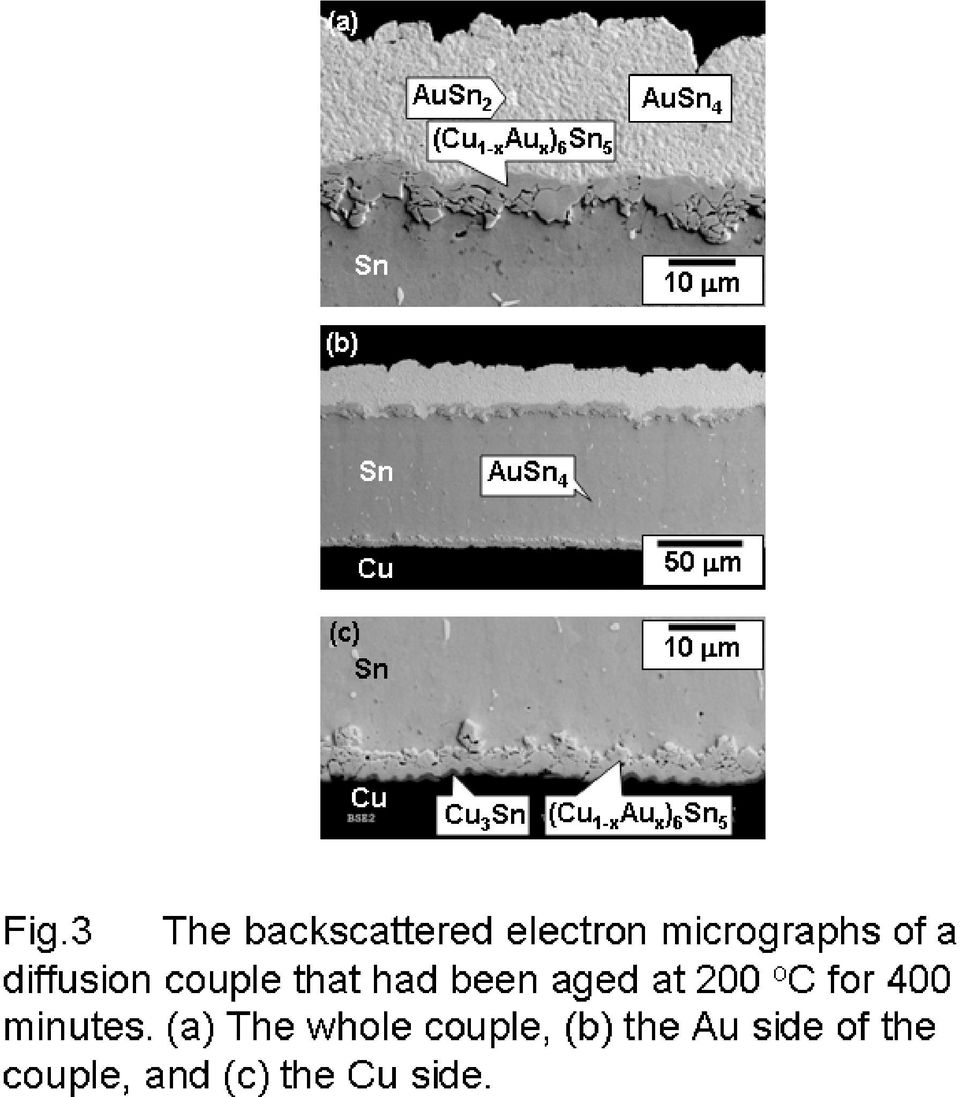
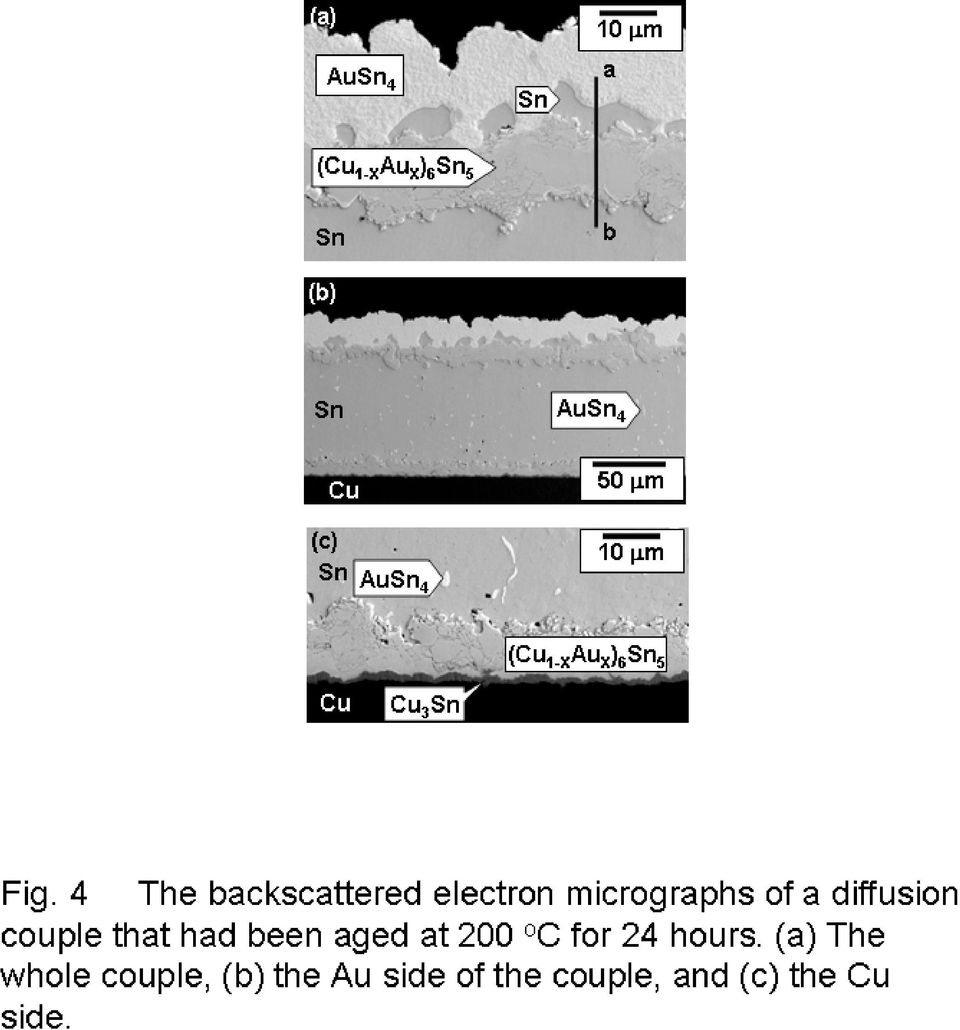
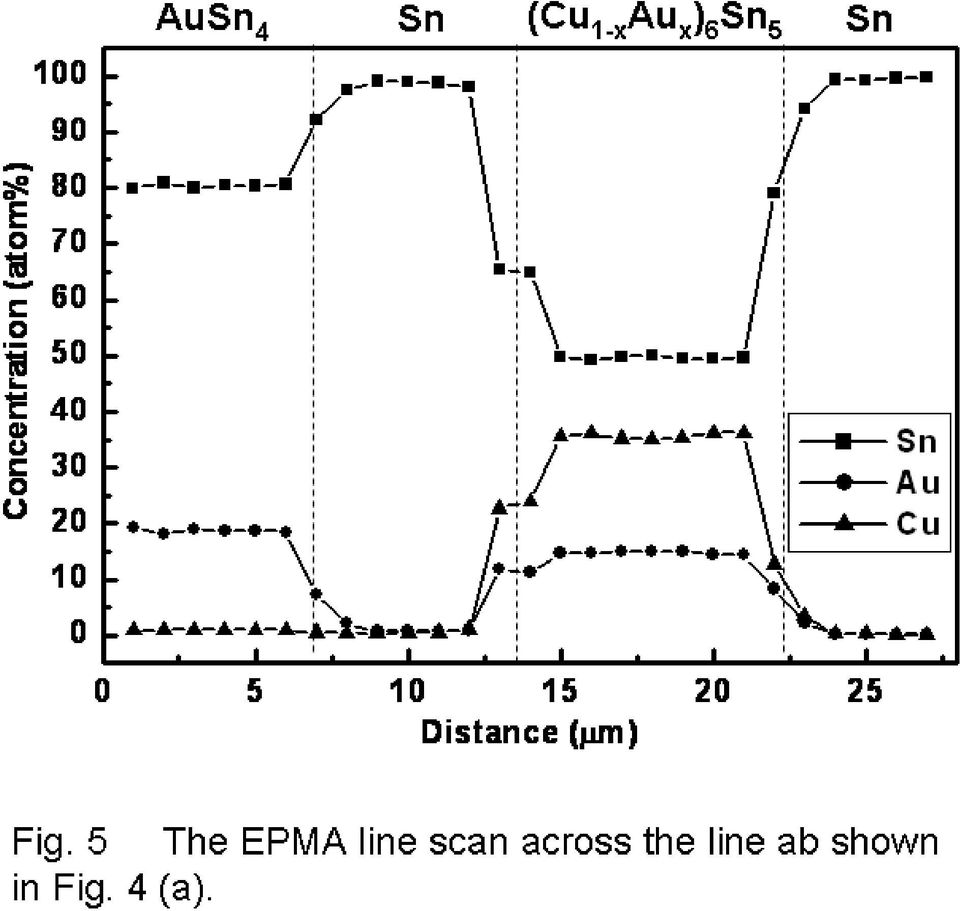
5 as shown in Fig. 3. The entire Au layer had been consumed, and even the AuSn phase had disappeared completely. Bulk of the remaining Au-Sn binary compound was AuSn 4, and a few isolated AuSn 2 embedded in AuSn 4 still existed. The amount of (Cu 1-x Au x ) 6 Sn 5 on the Au side of the original diffusion couple increased and became a continuous layer. On the opposite side (Cu side) shown in Fig. 3 (c), the thickness of (Cu 1-x Au x ) 6 Sn 5 also increased. Moreover, a layer of Cu 3 Sn formed between (Cu 1-x Au x ) 6 Sn 5 and Cu. When the aging time reached 24 hours (Fig. 4), AuSn 2 had disappeared completely as shown in Fig. 4 (a). Interestingly, there was a discontinuous Sn phase between AuSn 4 and (Cu 1-x Au x ) 6 Sn 5. An EPMA line scan was performed along the line ab marked in Fig. 4 (a), and the concentration profile is shown in Fig. 5. From the EPMA measurement, the composition of (Cu 1-x Au x ) 6 Sn 5 was determined to be 14.7 at.%, Au, 35.8 at.% Cu, and 49.5 at.% Sn. According to the 190 o C Au-Cu-Sn isotherm determined by Zakel [16] and reproduced in Fig. 6, this composition corresponded to the composition of (Cu 1-x Au x ) 6 Sn 5 at the Sn-AuSn 4 -(Cu 1-x Au x ) 6 Sn 5 three-phase equilibrium. As for the reaction on the Cu side, the thickness of (Cu 1-x Au x ) 6 Sn 5 as well as Cu 3 Sn increased as the reaction time increased, as shown in Fig. 4 (c). The (Cu 1-x Au x ) 6 Sn 5 phase now had substantial amount of Au dissolved (x= 0.23~0.25), but Au was still not detected in Cu 3 Sn. In Fig. 4 (b), one also noticed that there were AuSn 4 particles inside the Sn layer. The existence of these particles will be explained in the discussion section. As shown in Table I, the composition of (Cu 1-x Au x ) 6 Sn 5 did not change with the reaction time. The thickness of (Cu 1-x Au x ) 6 Sn 5 on the Au side as well as that on the Cu side is plotted against the square root of time in Fig. 7. Also shown in Fig. 7 is the thickness of Cu 6 Sn 5 from the binary Sn/Cu diffusion couple. The configuration, preparation, and aging treatment of these binary diffusion couples were the same as those of the Au/Sn/Cu ternary diffusion 5
, the thickness of (Cu 1-x Au x ) 6 Sn 5 also increased. Moreover, a layer of Cu 3 Sn formed between (Cu 1-x Au x ) 6 Sn 5 and Cu. When the aging time reached 24 hours (Fig.")
6 couples, except that the Au layer was not deposited. As can be seen in Fig. 7, (Cu 1-x Au x ) 6 Sn 5 on the Au side was the thickest, while (Cu 1-x Au x ) 6 Sn 5 on the Cu side is the thinnest. The data in Fig. 7 is summarized in Table II. 4. Discussion The Au-Sn-Cu phase diagram had been studied by Roeder at 170 o C [19] and by Zakel at 190 o C [16]. The one determined by Zakel (redrawn in Fig. 6) is to be used for the discussion as the temperature (190 o C) is closer to our experimental condition. In Figure 6, a diffusion path for the diffusion couple that had been aged for 24 hours is also shown. One question naturally arise is that why AuSn 4 on the Au side was covered with a layer of (Cu 1-x Au x ) 6 Sn 5, while those AuSn 4 particles inside the Sn layer was not, even though these particles located closer to the Cu source? The diffusion path shown in Fig. 6 clearly rationalized that such diffusion path was allowed. In other words, such feature was not forbidden for ternary diffusion couples. The thicknesses of (Cu 1-x Au x ) 6 Sn 5 under various conditions were shown in Fig. 7. The three sets of data all seemed to follow the parabolic kinetics. The (Cu 1-x Au x ) 6 Sn 5 on the Au side was the thickest, while that on the Cu side was the thinnest. The total consumption of the Cu foil corresponded to the formation of (Cu 1-x Au x ) 6 Sn 5 on the Au side and the Cu side. Comparing the amounts of this compound formed for the case with and without the Au layer, the existence of the Au layer clearly accelerated the Cu consumption. Apparently, the existence of the Au layer provided extra driving force, which accelerated the Cu consumption. The data in Fig. 7 and also enables us to calculate the Au flux and Cu flux across the Sn 6

7 layer. This is because the solubilities of Au and Cu in Sn are very low, about 0.2 at.% for Au in solid Sn at 200 o C [20] and 0.01 at.% for Cu in solid Sn at 227 o C [21], and consequently the amounts of Cu and Au present in the Sn layer can be ignored. We also neglected the Au present in the form of AuSn 4 inside the Sn layer. From the EPMA measurement, the compositions of the (Cu 1-x Au x ) 6 Sn 5 phase on both sides were known. With these assumptions, the integration of the Au flux over time correspond to the amount of Au that was incorporated into (Cu 1-x Au x ) 6 Sn 5 on the Cu side per unit area, and the integration of the Cu flux over time corresponded to the amount of Cu presented in (Cu 1-x Au x ) 6 Sn 5 on the Au side per unit area. Therefore, the derivative of the thickness versus time data will produce the flux at any instant. The resulting Au flux and Cu flux calculated this way versus time are shown in Fig. 8 and Table III. In calculating Fig. 8, the density for (Cu 1-x Au x ) 6 Sn 5 was needed. The binary compound Cu 6 Sn 5 was reported to have a density of 8.28 g/cm 3 [22]. The density of (Cu 1-x Au x ) 6 Sn 5 will increase slightly because Au is a heavier atom. We estimated the density of (Cu 0.7 Au 0.3 ) 6 Sn 5 to be about 8.8 g/cm 3, by using the lattice constant values for (Cu 0.7 Au 0.3 ) 6 Sn 5 measured in this study (a= nm and c= nm). It can be seen that the Cu flux through the Sn layer was about 2-3 times higher than the Au flux at any moment. According to the literature data, at 200 o C the diffusivity of Au along the c axis of Sn is (m 2 /sec) [23] and that of Cu along the c axis of Sn is (m 2 /sec) [24]. The diffusivity of Cu in Sn is one order of magnitude larger than the diffusivity of Au. The relative values for Au and Cu along other directions exhibits similar ration. Apparently, the difference in the values of the diffusivity is larger than that of the atomic flux. The difference between the relative magnitude of the flux and the diffusivity is probably due to the different driving forces for the diffusion of Au and Cu across the Sn layer. In Fig. 4 (a), there was Sn phase between AuSn 4 and (Cu 1-x Au x ) 6 Sn 5 interface. These Sn 7
 6 Sn 5 on the Cu side per unit area, and the integration of")
8 formed only after AuSn 2 had disappeared and AuSn 4 became the only Au-Sn binary compound. We believe these Sn came from the decomposition of the AuSn 4 phase. The AuSn 4 phase had to decompose to release Au, so that Au can reacted with the incoming Cu to form (Cu 1-x Au x ) 6 Sn 5. In other words, (Cu 1-x Au x ) 6 Sn 5 grew in the expense of AuSn 4. In fact, if we let the reaction continue, all AuSn 4 will be consumed, and the only compound left at that interface will be (Cu 1-x Au x ) 6 Sn 5. The released Sn from the decomposition accumulated and became the Sn phase. 5. Conclusion At 200 o C, the Cu atoms could diffuse through the 100 µm Sn layer and resulted in the formation of the (Cu 1-x Au x ) 6 Sn 5 on the Au side in 10 minutes. Under the same conditions, the Au atoms could diffuse through the Sn layer and became incorporated in the Cu 6 Sn 5 compound. These are evidences showing that Au and Cu can cross-interact across a distance of 100 µm even when Sn is in the solid state. During the joining process by soldering, the solder becomes molten and the cross-interaction becomes even more substantial. Consequently, the results of this study shows that the cross-interaction of Au and Cu in solders is extremely rapid, and cannot be ignored in those solder joints that have both elements present. Acknowledgment. This work was supported by the National Science Council of R.O.C. through grants NSC E and NSC E The authors thank Chung-Yuan, Kao (NTU) for assistance in EPMA measurements. 8

9 References 1. C. E. Ho, Y. M. Chen, and C. R. Kao, J. Electron. Mater., 28, p.1231, C. E. Ho, R. Zheng, G. L. Luo, A. H. Lin, and C. R. Kao, J. Electron. Mater., 29, p.1175, S. W. Chen, and Y. W. Yen, J. of Electron. Mater., 30, p.1133, C. E. Ho, S. Y. Tsai, and C. R. Kao, IEEE Trans. Adv. Packaging, 24, p.493, C. E. Ho, W. T. Chen, and C. R. Kao, J. Electron. Mater., 30, p.379, C. M. Liu, C. E. Ho, W. T. Chen, and C. R. Kao, J. Electron. Mater., 30, p. 1152, T. Y. Lee, W. J. Choi, K. N. Tu, J. W. Jang, S. M. Kuo, J. K. Lin, D. R. Frear, K. Zeng, and J. K. Kivilahti, J. Mater. Res., 17, p.291, L. C. Shiau, C. E. Ho, and C. R. Kao, Solder. Surf. Mt. Tech., 14, p.25, C. E. Ho, L. C. Shiau, and C. R. Kao, J. Electron. Mater., 31, p.1264, C. B. Lee, J. W. Yoon, S. J. Suh, S. B. Jung, C. W. Yang, C. C. Shur, and Y. E. Shin, J. Mater. Sci., 14, p.487, C. E. Ho, Y. L. Lin, J. Y. Tsai, and C. R. Kao, J. Chin. Inst. Chem. Eng., 34, p.387, T. Laurila, V. Vuorinen, T. Mattila, and J. K. Kivilahti, J. Electron. Mater., 34, p.103, J. Y. Tsai, C. W. Chang, Y. C. Shieh, Y. C. Hu, and C. R. Kao, J. Electron. Mater., 34, in press (February issue), Y. L. Lin, W. C. Luo, Y. H. Lin, C. E. Ho, and C. R. Kao, J. Electron. Mater., 33, p.1092,

10 15. E. Zakel and H. Reichl, in Flip Chip Technologies, ed. By J. H. Lau, Chapter 15, McGraw-Hill, New York, E. Zakel, thesis, Technical University-Berlin, C. M. Tsai, W. C. Luo, C. W. Chang, Y. C. Shieh, and C. R. Kao, J. Electron. Mater., 33, p.1424, P. G. Kim and K. N. Tu, J. Appl. Phys., 80, p.3822, J. Roeder, Doctoral Dissertation, Lehigh University, H. Okamoto and T. B. Massalski, eds., Phase Diagram of Binary Gold Alloys, ASM International, Metals Park, OH, p.278, C. E. Homer and H. Plummer, J. Inst. Met., 64, p.169, H. P. R. Frederikse, R. J. Fields, and A. Feldman, J. App. Phys., p2879, B. F. Dyson, J. Appl. Phys., p. 2375, B. F. Dyson, T. R. Anthony, and D. Turnbull, J. Appl. Phys., p. 3408, Figure Captions 10

11 Fig. 1 The microstructure of the as-deposited Au/Sn/Cu ternary diffusion couple. The Au layer was seven µm thick, and the Sn layer was 100 µm. Fig. 2 The backscattered electron micrographs of a diffusion couple that had been aged at 200 o C for 10 minutes. (a) The Au side of the couple, (b) the whole couple, and (c) the Cu side. Fig.3 The backscattered electron micrographs of a diffusion couple that had been aged at 200 o C for 400 minutes. (a) The Au side of the couple, (b) the whole couple, and (c) the Cu side. Fig. 4 The backscattered electron micrographs of a diffusion couple that had been aged at 200 o C for 24 hours. (a) The Au side of the couple, (b) the whole couple, and (c) the Cu side. Fig. 5 The EPMA line scan across the line ab shown in Fig. 4 (a). Fig. 6 The Au-Cu-Sn ternary isotherm at 190 o C. This isotherm was redrawn from the one determined by Zakel [16]. Fig. 7 The thickness of (Cu 1-x Au x ) 6 Sn 5 on the Au side, the thickness of (Cu 1-x Au x ) 6 Sn 5 on the Cu side, and the thickness of Cu 6 Sn 5 from the binary Sn/Cu diffusion couple versus the aging time. Fig. 8 The Au flux and the Cu flux across the Sn layer versus the aging time. Table I - The values of x in (Cu 1-x Au x ) 6 Sn 5 after 1, 24, and 189 hours. 11
 The Au side of the couple, (b) the whole couple, and (c) the Cu side. Fig.")
12 x value in (Cu 1-x Au x ) 6 Sn 5 1 hrs 24 hrs 189 hrs Au side Cu side

13 Table II Thickness of (Cu 1-x Au x ) 6 Sn 5 in Au/Sn/Cu diffusion couple and Sn/Cu diffusion couple at 200 o C. Time (Cu 1-x Au x ) 6 Sn 5 at Au/Sn/Cu (µm) Cu 6 Sn 5 at Sn/Cu (µm) (min) Cu side Au side

14 Table III- The Au flux and the Cu flux across the Sn layer in the Au/Sn/Cu diffusion couple at 200 o C. Time (min) Au flux Cu flux (atoms/cm 2 sec) (atoms/cm 2 sec)

15

16

17
18
19
20

21
22
Influence of Solder Reaction Across Solder Joints
 Influence of Solder Reaction Across Solder Joints Kejun Zeng FC BGA Packaging Development Semiconductor Packaging Development Texas Instruments, Inc. 6 th TRC Oct. 27-28, 2003 Austin, TX 1 Outline Introduction
Interfacial Reaction between Sn Ag Co Solder and Metals
 Materials Transactions, Vol. 46, No. 11 (25) pp. 2394 to 2399 Special Issue on Lead-Free ing in Electronics III #25 The Japan Institute of Metals Interfacial Reaction between Sn Ag Co and Metals Hiroshi
Materials Chemistry and Physics 85 (2004) 63 67. Meng-Kuang Huang, Pei-Lin Wu, Chiapyng Lee
 63 67. Meng-Kuang Huang, Pei-Lin Wu, Chiapyng Lee") Materials Chemistry and Physics 85 (2004) 63 67 Effects of different printed circuit board surface finishes on the formation and growth of intermetallics at thermomechanically fatigued small outline J
Materials Chemistry and Physics 85 (2004) 63 67 Effects of different printed circuit board surface finishes on the formation and growth of intermetallics at thermomechanically fatigued small outline J
Interface Reaction and Mechanical Properties of Lead-free Sn Zn Alloy/Cu Joints
 Materials Transactions, Vol. 43, No. 8 (2002) pp. 1797 to 1801 Special Issue on Lead-Free Electronics Packaging c 2002 The Japan Institute of Metals Interface Reaction and Mechanical Properties of Lead-free
REACTIONS IN THE SN CORNER OF THE CU-SN-ZN ALLOY SYSTEM
 REACTIONS IN THE SN CORNER OF THE CU-SN-ZN ALLOY SYSTEM D.D. Perovic, L Snugovsky and J.W. Rutter Department of Materials Science and Engineering University of Toronto Toronto, ON, Canada [email protected]
Effect of PWB Plating on the Microstructure and Reliability of SnAgCu Solder Joints
 Effect of PWB Plating on the Microstructure and Reliability of SnAgCu Solder Joints Y. Zheng, C. Hillman, P. McCluskey CALCE Electronic Products and Systems Center A. James Clark School of Engineering
The Interactions between SNAGCU Solder and NI(P)/AU, NI(P)/PD/AU UBMS
/AU, NI(P)/PD/AU UBMS") The Interactions between SNAGCU Solder and NI(P)/AU, NI(P)/PD/AU UBMS Jui-Yun Tsai, Josef Gaida, Gerhard Steinberger and Albrecht Uhlig Atotech Deutschland GmbH Berlin, Germany ABSTRACT The metallurgical
The Interactions between SNAGCU Solder and NI(P)/AU, NI(P)/PD/AU UBMS Jui-Yun Tsai, Josef Gaida, Gerhard Steinberger and Albrecht Uhlig Atotech Deutschland GmbH Berlin, Germany ABSTRACT The metallurgical
, Yong-Min Kwon 1 ) , Ho-Young Son 1 ) , Jeong-Tak Moon 2 ) Byung-Wook Jeong 2 ) , Kyung-In Kang 2 )
 , Ho-Young Son 1 ) , Jeong-Tak Moon 2 ) Byung-Wook Jeong 2 ) , Kyung-In Kang 2 )") Effect of Sb Addition in Sn-Ag-Cu Solder Balls on the Drop Test Reliability of BGA Packages with Electroless Nickel Immersion Gold (ENIG) Surface Finish Yong-Sung Park 1 ), Yong-Min Kwon 1 ), Ho-Young
Effect of Sb Addition in Sn-Ag-Cu Solder Balls on the Drop Test Reliability of BGA Packages with Electroless Nickel Immersion Gold (ENIG) Surface Finish Yong-Sung Park 1 ), Yong-Min Kwon 1 ), Ho-Young
Characterization and Kinetics of the Interfacial Reactions in Solder Joints of Tin-Based Solder Alloys on Copper Substrates
 Characterization and Kinetics of the Interfacial Reactions in Solder Joints of Tin-Based Solder Alloys on Copper Substrates J. C. Madeni*, S. Liu* and T. A. Siewert** *Center for Welding, Joining and Coatings
Interfacial Reactions Between Sn 58 mass%bi Eutectic Solder and (Cu, Electroless Ni P/Cu) Substrate
 Substrate") Materials Transactions, Vol. 43, No. 8 (2002) pp. 1821 to 1826 Special Issue on Lead-Free Electronics Packaging c 2002 The Japan Institute of Metals Interfacial Reactions Between Sn 58 mass%bi Eutectic
Materials Transactions, Vol. 43, No. 8 (2002) pp. 1821 to 1826 Special Issue on Lead-Free Electronics Packaging c 2002 The Japan Institute of Metals Interfacial Reactions Between Sn 58 mass%bi Eutectic
Interfacial Properties of Zn Sn Alloys as High Temperature Lead-Free Solder on Cu Substrate
 Materials Transactions, Vol. 46, No. 11 (2005) pp. 2413 to 2418 Special Issue on Lead-Free Soldering in Electronics III #2005 The Japan Institute of Metals Interfacial Properties of Zn Sn Alloys as High
Sn-Cu Intermetallic Grain Morphology Related to Sn Layer Thickness
 Journal of ELECTRONIC MATERIALS, Vol. 36, No. 11, 2007 DOI: 10.1007/s11664-007-0270-x Ó 2007 TMS Special Issue Paper -Cu Intermetallic Grain Morphology Related to Layer Thickness MIN-HSIEN LU 1 and KER-CHANG
Formation of Sn dendrites and SnAg eutectics in a SnAgCu solder
 Loughborough University Institutional Repository Formation of Sn dendrites and SnAg eutectics in a SnAgCu solder This item was submitted to Loughborough University's Institutional Repository by the/an
Phase formation between lead-free Sn Ag Cu solder and Ni P /Au finishes
 Reprinted with permission from Journal of Applied Physics, 99, 2, (2006), pp. 3530-3536. Copyright 2006, American Institute of Physics. JOURNAL OF APPLIED PHYSICS 99, 023530 2006 Phase formation between
Electromigration statistics and damage evolution for Pb-free solder joints with Cu and Ni UBM in plastic flip-chip packages
 J Mater Sci: Mater Electron (27) 8:247 258 DOI.7/s854-6-26-2 Electromigration statistics and damage evolution for Pb-free solder joints with Cu and in plastic flip-chip packages Seung-Hyun Chae Æ Xuefeng
Optical and Auger Microanalyses of Solder Adhesion Failures in Printed Circuit Boards
 Optical and Auger Microanalyses of Solder Adhesion Failures in Printed Circuit Boards K. Kumar and A. Moscaritolo The Charles Stark Draper Laboratory, Incorporated, Cambridge, Massachusetts 02139 ABSTRACT
Review of the Impact of Intermetallic Layers on the Brittleness of Tin-Lead and Lead-Free Solder Joints
 Review of the Impact of Intermetallic Layers on the Brittleness of Tin-Lead and Lead-Free Solder Joints Per-Erik Tegehall, Ph.D. 6-03-15 Preface This review has been funded by Vinnova (Swedish Governmental
Solutions without Boundaries. PCB Surface Finishes. Todd Henninger, C.I.D. Sr. Field Applications Engineer Midwest Region
 Solutions without Boundaries PCB Surface Finishes Todd Henninger, C.I.D. Sr. Field Applications Engineer Midwest Region 1 Notice Notification of Proprietary Information: This document contains proprietary
Electrical Characteristics for Sn-Ag-Cu Solder Bump with Ti/Ni/Cu Under-Bump Metallization after Temperature Cycling Tests
 Journal of ELECTRONIC MATERIALS, Vol. 35, No. 10, 2006 Regular Issue Paper Electrical Characteristics for Sn-Ag-Cu Solder Bump with Ti/Ni/Cu Under-Bump Metallization after Temperature Cycling Tests T.I.
Phase. Gibbs Phase rule
 Phase diagrams Phase A phase can be defined as a physically distinct and chemically homogeneous portion of a system that has a particular chemical composition and structure. Water in liquid or vapor state
LOGO. Modeling and Simulation of Microstructural Changes in Composite Sn-Ag-Cu Solder Alloys with Cu Nanoparticles
 Modeling and Simulation of Microstructural Changes in Composite Sn-Ag-Cu Solder Alloys with Cu Nanoparticles Yuanyuan Guan, A.Durga, Nele Moelans Dept. Metallurgy and Materials Engineering, K.U. Leuven,
Analysis of BGA Solder Joint Reliability for Selected Solder Alloy and Surface Finish Configurations
 Analysis of BGA Solder Joint Reliability for Selected Solder Alloy and Surface Finish Configurations Hugh Roberts / Atotech USA Inc Sven Lamprecht and Christian Sebald / Atotech Deutschland GmbH Mark Bachman,
Chapter 8. Phase Diagrams
 Phase Diagrams A phase in a material is a region that differ in its microstructure and or composition from another region Al Al 2 CuMg H 2 O(solid, ice) in H 2 O (liquid) 2 phases homogeneous in crystal
Thermodynamic database of the phase diagrams in copper base alloy systems
 Journal of Physics and Chemistry of Solids 66 (2005) 256 260 www.elsevier.com/locate/jpcs Thermodynamic database of the phase diagrams in copper base alloy systems C.P. Wang a, X.J. Liu b, M. Jiang b,
Chapter Outline. Diffusion - how do atoms move through solids?
 Chapter Outline iffusion - how do atoms move through solids? iffusion mechanisms Vacancy diffusion Interstitial diffusion Impurities The mathematics of diffusion Steady-state diffusion (Fick s first law)
SELECTIVE DISSOLUTION AND CORROSION FATIGUE BEHAVIORS OF 2205 DUPLEX STAINLESS STEEL
 W.-T. Tsai, I.-H. Lo Department of Materials Science and Engineering National Cheng Kung University Tainan, Taiwan SELECTIVE DISSOLUTION AND CORROSION FATIGUE BEHAVIORS OF 2205 DUPLEX STAINLESS STEEL ABSTRACT
Thermomigration of Cu Sn and Ni Sn intermetallic compounds during electromigration in Pb-free SnAg solder joints
 Thermomigration of Cu Sn and Ni Sn intermetallic compounds during electromigration in Pb-free SnAg solder joints Hsiao-Yun Chen and Chih Chen a) Department of Materials Science and Engineering, National
Phase Equilibria & Phase Diagrams
 Phase Equilibria & Phase Diagrams Week7 Material Sciences and Engineering MatE271 1 Motivation Phase diagram (Ch 9) Temperature Time Kinematics (Ch 10) New structure, concentration (mixing level) (at what
Composite Electromagnetic Wave Absorber Made of Permalloy or Sendust and Effect of Sendust Particle Size on Absorption Characteristics
 PIERS ONLINE, VOL. 4, NO. 8, 2008 846 Composite Electromagnetic Wave Absorber Made of Permalloy or Sendust and Effect of Sendust Particle Size on Absorption Characteristics K. Sakai, Y. Wada, and S. Yoshikado
Coating Thickness and Composition Analysis by Micro-EDXRF
 Application Note: XRF Coating Thickness and Composition Analysis by Micro-EDXRF www.edax.com Coating Thickness and Composition Analysis by Micro-EDXRF Introduction: The use of coatings in the modern manufacturing
Soldering Definition and Differences
 Soldering Understanding the Basics Copyright 2014 ASM International M. Schwartz, editor All rights reserved www.asminternational.org Chapter 1 Soldering Definition and Differences SOLDER IS A FUSIBLE METAL
Etching effects and the formation of Streaking Defects on Al Extrusions
 Etching effects and the formation of Streaking Defects on Al Extrusions Surface defects such as streaking are often present on anodized extrusions of 6xxx series alloys. The streak defect is the result
J H Liao 1, Jianshe Tang 2,b, Ching Hwa Weng 2, Wei Lu 2, Han Wen Chen 2, John TC Lee 2
 Solid State Phenomena Vol. 134 (2008) pp 359-362 Online available since 2007/Nov/20 at www.scientific.net (2008) Trans Tech Publications, Switzerland doi:10.4028/www.scientific.net/ssp.134.359 Metal Hard
Reliability of Eutectic Sn-Pb Solder Bumps and Flip Chip Assemblies
 Reliability of Eutectic Sn-Pb Solder Bumps and Flip Chip Assemblies Xingjia Huang 1, Christine Kallmayer 2, Rolf Aschenbrenner 2, S.-W. Ricky Lee 1 1 Department of Mechanical Engineering Hong Kong University
Laser sintering of greens compacts of MoSi 2
 Laser sintering of greens compacts of MoSi 2 G. de Vasconcelos 1, R. Cesar Maia 2, C.A.A.Cairo 3, R. Riva 2, N.A.S.Rodrigues 2, F.C.L.Mello 3 Instituto de Estudos Avançados 1, Instituto Tecnológico de
Effect of the oxide film formed on the electrical properties of Cu-Zn alloy electric contact material
 Effect of the oxide film formed on the electrical properties of Cu-Zn alloy electric contact material Hao-Long Chen *, Ke-Cheng Tseng and Yao-Sheng Yang Department of Electronic Engineering, Kao Yuan University,
PROTECTIVE LAYERS OF IRON AND NICKEL ALUMINIDES ON STEEL
 This work is licensed under the Creative Commons Attribution-NonCommercial-NoDerivs 3.0 Unported License. To view a copy of this license, visit http://creativecommons.org/licenses/by-nc-nd/3.0/ or send
Chapter 5: Diffusion. 5.1 Steady-State Diffusion
 : Diffusion Diffusion: the movement of particles in a solid from an area of high concentration to an area of low concentration, resulting in the uniform distribution of the substance Diffusion is process
Lead-Free Universal Solders for Optical and MEMS Packaging
 Lead-Free Universal Solders for Optical and MEMS Packaging Sungho Jin Univ. of California, San Diego, La Jolla CA 92093 OUTLINE -- Introduction -- Universal Solder Fabrication -- Microstructure -- Direct
High Strength and Wear Resistant Aluminum Alloy for High Temperature Applications
 High Strength and Wear Resistant Aluminum Alloy for High Temperature Applications JONATHAN A. LEE NASA-Marshall Space Flight Center (MSFC) Mail Code ED33 Huntsville, AL 35812 Email: [email protected]
Lecture 19: Eutectoid Transformation in Steels: a typical case of Cellular
 Lecture 19: Eutectoid Transformation in Steels: a typical case of Cellular Precipitation Today s topics Understanding of Cellular transformation (or precipitation): when applied to phase transformation
DIFFUSION IN SOLIDS. Materials often heat treated to improve properties. Atomic diffusion occurs during heat treatment
 DIFFUSION IN SOLIDS WHY STUDY DIFFUSION? Materials often heat treated to improve properties Atomic diffusion occurs during heat treatment Depending on situation higher or lower diffusion rates desired
Lead Free Wave Soldering
 China - Korea - Singapore- Malaysia - USA - Netherlands - Germany WAVE SELECTIVE REFLOW SOLDERING SOLDERING SOLDERING Lead Free Wave Soldering Ursula Marquez October 18, 23 Wave Soldering Roadmap Parameter
Good Boards = Results
 Section 2: Printed Circuit Board Fabrication & Solderability Good Boards = Results Board fabrication is one aspect of the electronics production industry that SMT assembly engineers often know little about.
Effect of Consolidation Process on Tensile Properties of Fe Cu P/M Alloy from Rapidly Solidified Powder
 Materials Transactions, Vol. 44, No. 7 (2003) pp. 1311 to 1315 Special Issue on Growth of Ecomaterials as a Key to Eco-Society #2003 The Japan Institute of Metals Effect of Consolidation Process on Tensile
Introduction to Materials Science, Chapter 9, Phase Diagrams. Phase Diagrams. University of Tennessee, Dept. of Materials Science and Engineering 1
 Phase Diagrams University of Tennessee, Dept. of Materials Science and Engineering 1 Chapter Outline: Phase Diagrams Microstructure and Phase Transformations in Multicomponent Systems Definitions and basic
How do single crystals differ from polycrystalline samples? Why would one go to the effort of growing a single crystal?
 Crystal Growth How do single crystals differ from polycrystalline samples? Single crystal specimens maintain translational symmetry over macroscopic distances (crystal dimensions are typically 0.1 mm 10
EFFECT OF Au-INTERMETALLIC COMPOUNDS ON MECHANICAL RELIABILITY OF Sn-Pb/Au-Ni-Cu JOINTS
 EFFECT OF Au-INTERMETALLIC COMPOUNDS ON MECHANICAL RELIABILITY OF Sn-Pb/Au-Ni-Cu JOINTS A. Zribi, R.R. Chromik, R. Presthus, J.Clum, L. Zavalij and E.J. Cotts Binghamton University; Physics Dept.; P.O.
MICROALLOYED Sn-Cu Pb-FREE SOLDER FOR HIGH TEMPERATURE APPLICATIONS
 MICROALLOYED Sn-Cu Pb-FREE SOLDER FOR HIGH TEMPERATURE APPLICATIONS Keith Howell 1, Keith Sweatman 1, Motonori Miyaoka 1, Takatoshi Nishimura 1, Xuan Quy Tran 2, Stuart McDonald 2, and Kazuhiro Nogita
RAPIDLY SOLIDIFIED COPPER ALLOYS RIBBONS
 Association of Metallurgical Engineers of Serbia AMES Scientific paper UDC:669.35-153.881-412.2=20 RAPIDLY SOLIDIFIED COPPER ALLOYS RIBBONS M. ŠULER 1, L. KOSEC 1, A. C. KNEISSL 2, M. BIZJAK 1, K. RAIĆ
Comparative Wetting Ability of Lead-Free Alloys
 Comparative Wetting Ability of Lead-Free Alloys Understanding the wetting kinetics of lead-free alloys becomes crucial in selecting a suitable lead-free composition for assembling PCBs. KaiHwa Chew, Vincent
Power Dissipation Considerations in High Precision Vishay Sfernice Thin Film Chips Resistors and Arrays (P, PRA etc.) (High Temperature Applications)
 (High Temperature Applications)") VISHAY SFERNICE Resistive Products Application Note ABSTRACT On our thin film chips resistors and arrays the main path for the heat, more than 90 %, is conduction through the body of the component, the
VISHAY SFERNICE Resistive Products Application Note ABSTRACT On our thin film chips resistors and arrays the main path for the heat, more than 90 %, is conduction through the body of the component, the
Mounting Instructions for SP4 Power Modules
 Mounting Instructions for SP4 Power Modules Pierre-Laurent Doumergue R&D Engineer Microsemi Power Module Products 26 rue de Campilleau 33 520 Bruges, France Introduction: This application note gives the
ENIG with Ductile Electroless Nickel for Flex Circuit Applications
 ENIG with Ductile Electroless Nickel for Flex Circuit Applications Yukinori Oda, Tsuyoshi Maeda, Chika Kawai, Masayuki Kiso, Shigeo Hashimoto C.Uyemura & Co., Ltd. George Milad and Donald Gudeczauskas
Improved Contact Formation for Large Area Solar Cells Using the Alternative Seed Layer (ASL) Process
 Process") Improved Contact Formation for Large Area Solar Cells Using the Alternative Seed Layer (ASL) Process Lynne Michaelson, Krystal Munoz, Jonathan C. Wang, Y.A. Xi*, Tom Tyson, Anthony Gallegos Technic Inc.,
Improved Contact Formation for Large Area Solar Cells Using the Alternative Seed Layer (ASL) Process Lynne Michaelson, Krystal Munoz, Jonathan C. Wang, Y.A. Xi*, Tom Tyson, Anthony Gallegos Technic Inc.,
Effects of Alloying in Near-Eutectic Tin Silver Copper Solder Joints
 Materials Transactions, Vol. 43, No. 8 (2002) pp. 1827 to 1832 Special Issue on Lead-Free Electronics Packaging c 2002 The Japan Institute of Metals Effects of Alloying in Near-Eutectic Tin Silver Copper
PRINTED CIRCUIT BOARD SURFACE FINISHES - ADVANTAGES AND DISADVANTAGES
 PRINTED CIRCUIT BOARD SURFACE FINISHES - ADVANTAGES AND DISADVANTAGES By Al Wright, PCB Field Applications Engineer Epec Engineered Technologies Anyone involved within the printed circuit board (PCB) industry
Choosing a Low-Cost Alternative to SAC Alloys for PCB Assembly
 Choosing a Low-Cost Alternative to SAC Alloys for PCB Assembly Our thanks to Indium Corporation for allowing us to reprint the following article. By Brook Sandy and Ronald C. Lasky, PhD, PE., Indium Corporation
Process Parameters Optimization for Friction Stir Welding of Pure Aluminium to Brass (CuZn30) using Taguchi Technique
 using Taguchi Technique") MATEC Web of Conferences43, 03005 ( 016) DOI: 10.1051/ matecconf/ 016 4303005 C Owned by the authors, published by EDP Sciences, 016 Process Parameters Optimization for Friction Stir Welding of Pure Aluminium
MATEC Web of Conferences43, 03005 ( 016) DOI: 10.1051/ matecconf/ 016 4303005 C Owned by the authors, published by EDP Sciences, 016 Process Parameters Optimization for Friction Stir Welding of Pure Aluminium
Defects Introduction. Bonding + Structure + Defects. Properties
 Defects Introduction Bonding + Structure + Defects Properties The processing determines the defects Composition Bonding type Structure of Crystalline Processing factors Defects Microstructure Types of
Pb-Free Plating for Electronic Components
 Pb-Free Plating for Electronic Components by Morimasa Tanimoto *, Hitoshi Tanaka *, Satoshi Suzuki * and Akira Matsuda * The authors have developed Pb-free tin alloy plating materials. Preliminary ABSTRACT
LEAD FREE HALOGENFREE. Würth Elektronik PCB Design Conference 2007. Lothar Weitzel 2007 Seite 1
 LEAD FREE HALOGENFREE Würth Elektronik PCB Design Conference 2007 Lothar Weitzel 2007 Seite 1 Content Solder surfaces/overview Lead free soldering process requirements/material parameters Different base
10.7 Kinetic Molecular Theory. 10.7 Kinetic Molecular Theory. Kinetic Molecular Theory. Kinetic Molecular Theory. Kinetic Molecular Theory
 The first scheduled quiz will be given next Tuesday during Lecture. It will last 5 minutes. Bring pencil, calculator, and your book. The coverage will be pp 364-44, i.e. Sections 0.0 through.4. 0.7 Theory
EXPERIMENTAL STUDY OF STRUCTURAL ZONE MODEL FOR COMPOSITE THIN FILMS IN MAGNETIC RECORDING MEDIA APPLICATION
 EXPERIMENTAL STUDY OF STRUCTURAL ZONE MODEL FOR COMPOSITE THIN FILMS IN MAGNETIC RECORDING MEDIA APPLICATION Hua Yuan and David E. Laughlin Department of Materials Science and Engineering, Carnegie Mellon
h e l p s y o u C O N T R O L
 contamination analysis for compound semiconductors ANALYTICAL SERVICES B u r i e d d e f e c t s, E v a n s A n a l y t i c a l g r o u p h e l p s y o u C O N T R O L C O N T A M I N A T I O N Contamination
Introduction to VLSI Fabrication Technologies. Emanuele Baravelli
 Introduction to VLSI Fabrication Technologies Emanuele Baravelli 27/09/2005 Organization Materials Used in VLSI Fabrication VLSI Fabrication Technologies Overview of Fabrication Methods Device simulation
Evaluating Surface Roughness of Si Following Selected Lapping and Polishing Processes
 Applications Laboratory Report 86 Evaluating Surface Roughness of Si Following Selected Processes Purpose polishing of samples is a common application and required for a variety of manufacturing and research
Objectives/Introduction Extraction of zinc Physical properties of zinc Zinc casting alloys Wrought zinc alloys Engineering design with zinc alloys
 Lecture 7 Zinc and its alloys Subjects of interest Objectives/Introduction Extraction of zinc Physical properties of zinc Zinc casting alloys Wrought zinc alloys Engineering design with zinc alloys Objectives
Vacuum Evaporation Recap
 Sputtering Vacuum Evaporation Recap Use high temperatures at high vacuum to evaporate (eject) atoms or molecules off a material surface. Use ballistic flow to transport them to a substrate and deposit.
Lecture: 33. Solidification of Weld Metal
 Lecture: 33 Solidification of Weld Metal This chapter presents common solidification mechanisms observed in weld metal and different modes of solidification. Influence of welding speed and heat input on
A New (Better) Approach to Tin Whisker Mitigation
 Approach to Tin Whisker Mitigation") A New (Better) Approach to Tin Whisker Mitigation Craig Hillman, Gregg Kittlesen, and Randy Schueller Environmental testing can only take the industry so far. A return to fundamentals promises better mitigation
A New (Better) Approach to Tin Whisker Mitigation Craig Hillman, Gregg Kittlesen, and Randy Schueller Environmental testing can only take the industry so far. A return to fundamentals promises better mitigation
Wetting Behavior of Pb-free Solder on Immersion Tin Surface Finishes in Different Reflow Atmospheres
 Wetting Behavior of Pb-free Solder on Immersion Tin Surface Finishes in Different Reflow Atmospheres Sven Lamprecht 1, Dr. Kenneth Lee 2, Bill Kao 3, Günter Heinz 1 1 Atotech Deutschland GmbH, Berlin,
Conductivity of silicon can be changed several orders of magnitude by introducing impurity atoms in silicon crystal lattice.
 CMOS Processing Technology Silicon: a semiconductor with resistance between that of conductor and an insulator. Conductivity of silicon can be changed several orders of magnitude by introducing impurity
The atomic packing factor is defined as the ratio of sphere volume to the total unit cell volume, or APF = V S V C. = 2(sphere volume) = 2 = V C = 4R
 = 2 = V C = 4R") 3.5 Show that the atomic packing factor for BCC is 0.68. The atomic packing factor is defined as the ratio of sphere volume to the total unit cell volume, or APF = V S V C Since there are two spheres associated
3.5 Show that the atomic packing factor for BCC is 0.68. The atomic packing factor is defined as the ratio of sphere volume to the total unit cell volume, or APF = V S V C Since there are two spheres associated
Chapter 12 - Liquids and Solids
 Chapter 12 - Liquids and Solids 12-1 Liquids I. Properties of Liquids and the Kinetic Molecular Theory A. Fluids 1. Substances that can flow and therefore take the shape of their container B. Relative
State of the art in reactive magnetron sputtering
 State of the art in reactive magnetron sputtering T. Nyberg, O. Kappertz, T. Kubart and S. Berg Solid State Electronics, The Ångström Laboratory, Uppsala University, Box 534, S-751 21 Uppsala, Sweden D.
Development of Sn-Zn-Al Lead-Free Solder Alloys
 Development of Sn-Zn-Al Lead-Free Solder Alloys V Masayuki Kitajima V Tadaaki Shono (Manuscript received January, 5) Fujitsu has implemented a company-wide effort to progressively reduce the use of lead
Friction Surfacing of Austenitic Stainless Steel on Low Carbon Steel: Studies on the Effects of Traverse Speed
 , June 30 - July 2, 2010, London, U.K. Friction Surfacing of Austenitic Stainless Steel on Low Carbon Steel: Studies on the Effects of Traverse Speed H. Khalid Rafi, G. D. Janaki Ram, G. Phanikumar and
BINARY SYSTEMS. Definition of Composition: Atomic (molar) fraction. Atomic percent. Mass fraction. Mass percent (weight percent)
 fraction. Atomic percent. Mass fraction. Mass percent (weight percent)") BINARY SYSTEMS Definition of Composition: Atomic (molar) fraction Atomic percent Mass fraction Mass percent (weight percent) na =, x i n = A i i i Weight percent mainly in industry! x at % A = x 100 A
BINARY SYSTEMS Definition of Composition: Atomic (molar) fraction Atomic percent Mass fraction Mass percent (weight percent) na =, x i n = A i i i Weight percent mainly in industry! x at % A = x 100 A
Plate waves in phononic crystals slabs
 Acoustics 8 Paris Plate waves in phononic crystals slabs J.-J. Chen and B. Bonello CNRS and Paris VI University, INSP - 14 rue de Lourmel, 7515 Paris, France [email protected] 41 Acoustics 8 Paris We
0.3 mm Contact Pitch, 0.9 mm above the board, Flexible Printed Circuit ZIF Connectors.
 0.3 mm Contact Pitch, 0.9 mm above the board, Flexible Printed Circuit ZIF Connectors. FH Series (51pos. type) 3.45mm 17.1mm 0.9mm Features 1. Extremely light weight The largest version, with all contacts
9.11 Upon heating a lead-tin alloy of composition 30 wt% Sn-70 wt% Pb from 150 C and utilizing Figure
 9-13 9.8: 9.11 Upon heating a lead-tin alloy of composition 30 wt% Sn-70 wt% Pb from 150 C and utilizing Figure (a) The first liquid forms at the temperature at which a vertical line at this composition
MICROSTRUCTURAL AND MECHANICAL CHARACTERIZATION OF GRAY CAST IRON AND AlSi ALLOY AFTER LASER BEAM HARDENING
 Materials Science Forum Vols. 638-642 (2010) pp 769-774 Online available since 2010/Jan/12 at www.scientific.net (2010) Trans Tech Publications, Switzerland doi:10.4028/www.scientific.net/msf.638-642.769
Ion Beam Sputtering: Practical Applications to Electron Microscopy
 Ion Beam Sputtering: Practical Applications to Electron Microscopy Applications Laboratory Report Introduction Electron microscope specimens, both scanning (SEM) and transmission (TEM), often require a
Scanning Electron Microscopy Services for Pharmaceutical Manufacturers
 Scanning Electron Microscopy Services for Pharmaceutical Manufacturers Author: Gary Brake, Marketing Manager Date: August 1, 2013 Analytical Testing Laboratory www.atl.semtechsolutions.com Scanning Electron
Lecture 18 Strain Hardening And Recrystallization
 -138- Lecture 18 Strain Hardening And Recrystallization Strain Hardening We have previously seen that the flow stress (the stress necessary to produce a certain plastic strain rate) increases with increasing
Pure Tin - The Finish of Choice for Connectors
 Pure Tin - The Finish of Choice for Connectors Pete Elmgren and Dan Dixon Molex Lisle, IL Robert Hilty, Ph.D. Tyco Electronics Harrisburg, PA Thomas Moyer and Sudarshan Lal, Ph.D. FCI Etters, PA Axel Nitsche
Types of Epitaxy. Homoepitaxy. Heteroepitaxy
 Epitaxy Epitaxial Growth Epitaxy means the growth of a single crystal film on top of a crystalline substrate. For most thin film applications (hard and soft coatings, optical coatings, protective coatings)
IN THE electronic packaging industry, high-integrity and. Characteristics of Sn Cu Solder Bump Formed by Electroplating for Flip Chip
 10 IEEE TRANSACTIONS ON ELECTRONICS PACKAGING MANUFACTURING, VOL. 29, NO. 1, JANUARY 2006 Characteristics of Sn Cu Solder Bump Formed by Electroplating for Flip Chip Seok Won Jung, Jae Pil Jung, and Y.
Basic Properties and Application of Auto Enamels
 Basic Properties and Application of Auto Enamels Composition of Ceramic Automotive Glass Enamels Ceramic automotive glass colours are glass enamels that fire on to the glass during the bending process
Current Measurement of Resistance Spot Welding Using DSP
 Tamkang Journal of Science and Engineering, Vol. 14, No. 1, pp. 33 38 (2011) 33 Current Measurement of Resistance Spot Welding Using DSP Wen-Ren Yang and Chau-Shing Wang* Department of Electrical Engineering,
Chapter 13 - LIQUIDS AND SOLIDS
 Chapter 13 - LIQUIDS AND SOLIDS Problems to try at end of chapter: Answers in Appendix I: 1,3,5,7b,9b,15,17,23,25,29,31,33,45,49,51,53,61 13.1 Properties of Liquids 1. Liquids take the shape of their container,
FEATURES AND BENEFITS OF DIFFERENT PLATINUM ALLOYS. Kris Vaithinathan and Richard Lanam Engelhard Corporation
 FEATURES AND BENEFITS OF DIFFERENT PLATINUM ALLOYS Kris Vaithinathan and Richard Lanam Engelhard Corporation Introduction There has been a significant increase in the world wide use of platinum for jewelry
DURABILITY OF MORTAR LININGS IN DUCTILE IRON PIPES Durability of mortar linings
 DURABILITY OF MORTAR LININGS IN DUCTILE IRON PIPES Durability of mortar linings I. S. MELAND SINTEF Civil and Environmental Engineering, Cement and Concrete, Trondheim, Norway Durability of Building Materials
Iron-Carbon Phase Diagram (a review) see Callister Chapter 9
 see Callister Chapter 9") Iron-Carbon Phase Diagram (a review) see Callister Chapter 9 University of Tennessee, Dept. of Materials Science and Engineering 1 The Iron Iron Carbide (Fe Fe 3 C) Phase Diagram In their simplest form,
Iron-Carbon Phase Diagram (a review) see Callister Chapter 9 University of Tennessee, Dept. of Materials Science and Engineering 1 The Iron Iron Carbide (Fe Fe 3 C) Phase Diagram In their simplest form,
FRETTING FATIGUE UNDER VARYING LOADING BELOW THE FRETTING FATIGUE LIMIT
 FRETTING FATIGUE UNDER VARYING LOADING BELOW THE FRETTING FATIGUE LIMIT Yoshiyuki KONDO 1, Chu SAKAE 1, Masanobu KUBOTA 1 and Hiroki KITAHARA 2 1 Kyushu University, Faculty of Engineering, 6-10-1, Hakozaki,