DATA SHEET. ( DOC No. HX8347-A01-DS ) HX8347-A01
|
|
|
- Letitia Holt
- 9 years ago
- Views:
Transcription
 HX8347-A01 240RGB x 320 dot, 262K color, with internal")
1 DATA SHEET ( DOC No. HX8347-A01-DS ) HX8347-A01 240RGB x 320 dot, 262K color, with internal GRAM, TFT Mobile Single Chip Driver Preliminary version 01

2 240RGB x 320 dot, 262K color, with internal GRAM, TFT Mobile Single Chip Driver List of Contents 1. General Description Features Display Display Module Display/Control Interface Miscellaneous Block Diagram Pin Description Pin Description Pin Assignment PAD Coordinates Alignment Mark Bump Size Function Description Interface Control Mode Register-Content Interface Mode Serial Bus System Interface RGB Interface Address Counter (AC) MCU to Memory Write/Read Direction Source, Gate and Memory Map Tearing Effect Output Line Tearing Effect Line Modes Tearing Effect Line Timing Example 1 MPU Write is faster than Panel Read Example 2 MPU Write is slower than Panel Read Oscillator Source Driver Gate Driver LCD Power Generation Circuit LCD Power Generation Scheme Various Boosting Steps Gray Voltage Generator for Source Driver Structure of Grayscale Voltage Generator Gamma-Characteristics Adjustment Register Gamma Macro Adjustment Registers Gamma Resister Stream and 8 to 1 Selector Variable Resister Scan Mode Setting Oscillator Register Setting Flow (Register-Content Interface mode only) Power Supply Setting Input / Output Pin State Output or Bi-directional (I/O) Pins Input Pins Programming sequence Programming circuitry Free Running Mode Specification Command Command Set Index Register Display Mode Control Register (R01h) Column Address Start Register (R02~03h) P.1-

3 240RGB x 320 dot, 262K color, with internal GRAM, TFT Mobile Single Chip Driver List of Contents 6.5 Column Address End Register (R04~05h) Row Address Start Register (R06~07h) Row Address End Register (R08~09h) Partial Area Start Row Register (R0A~0Bh) Partial Area End Row Register (R0C~0Dh) Vertical Scroll Top Fixed Area Register (R0E~0Fh) Vertical Scroll Height Area Register (R10~11h) Vertical Scroll Button Fixed Area Register (R12~13h) Vertical Scroll Start Address Register (R14~15h) Memory Access Control Register (R16h) Gate scan Control Register (R18h) OSC Control 1 Register (R19h) OSC Control Register 2 (R1Ah) Power Control 1 Register (R1Bh) Power Control 2 Register (R1Ch) Power Control 3 Register (R1Dh) Power Control 4 Register (R1Eh) Power Control 5 Register (R1Fh) Power Control 6 Register (R20h) Power Control 7 Register (R21h) Read Data Register (R22h) Cycle Control 1~3 Register (R23~25h) Display Control 1 Register (R26h) Display Control 2~7 Register (R27h~R2Ah, R2Ch, R2Dh) Power Control 11 Register (R2Bh) Display Control 9 Register (R35h) Display Control 10 Register (R36h) Display Control 12 Register (R37h) RGB Interface Control 1 Register (R38h) RGB Interface Control 2 Register (R39h) Cycle Control 1~3 Register (R3A~3Ch) Cycle Control 4 Register (R3Dh) Cycle Control 5 Register (R3Eh) Cycle Control 6 Register (R40h) Display Control 14 Register (R41h) BGP Control Register (R42h) Vcom Control 1 Register (R43h) Vcom Control 2 Register (R44h) Vcom Control 3 Register (R45h) GAMMA Control 1~12 Register (R46~51h) Internal Use 16 (R64h) Internal Use 17 (R65h) Internal Use 18 (R66h) Himax ID code (R67h) Internal Use 28 (R70h) Data control register (R72h) Display Control 8 (R90h) Display Control 11 (R91h) OSC Control 3 (R93h) SAP Idle Mode (R94h) DCCLK SYNC TO CL1 (R95h) Electrical Characteristic Absolute Maximum Ratings ESD Protection Level Latch-Up Protection Level P.2-
... 85 6.15 Gate scan Control Register (R18h)... 86 6.16 OSC Control 1 Register (R19h)... 86 6.17 OSC Control Register 2 (R1Ah)... 87 6.")
4 240RGB x 320 dot, 262K color, with internal GRAM, TFT Mobile Single Chip Driver List of Contents 7.4 Light Sensitivity Maximum Series Resistance DC Characteristics AC CHARACTERISTICS Parallel Interface Characteristics (8080-series MPU) Parallel Interface Characteristics (6800-series MPU) Serial Interface Characteristics RGB Interface Characteristics Reset Input Timing Reference Applications Register-Content Interface Mode External Components Connection Ordering Information Revision History P.3-

5 240RGB x 320 dot, 262K color, with internal GRAM, TFT Mobile Single Chip Driver List of Figures Figure 5. 1 Register Read/Write Timing in Parallel Bus System Interface (for I80 Series MPU) Figure 5. 2 GRAM Read/Write Timing in 16-/18-Bit Parallel Bus System Interface (for I80 Series MPU) Figure 5. 3 GRAM Read/Write Timing in 8-Bit Parallel Bus System Interface (for I80 Series MPU) 29 Figure 5. 4 Register Read/Write Timing in Parallel Bus System Interface (for M68 Series MPU) Figure 5. 5 GRAM Read/Write Timing in 16-/18-Bit Parallel Bus System Interface (for M68 Series MPU) Figure 5. 6 GRAM Read/Write Timing in 8-bit Parallel Bus System Interface (for M68 Series MPU) Figure 5. 7 Example of I80- / M68- System 16-Bit Parallel Bus Interface Figure 5. 8 Input Data Bus and GRAM Data Mapping in 18-Bit Bus System Interface ( BS2, BS1, BS0 = 010 or 101 ) Figure 5. 9 Example of I80- / M68- System 16-bit Parallel Bus Interface Figure Input Data Bus and GRAM Data Mapping in 16-Bit Bus System Interface with 16 Bit-Data Input ( BS2, BS1, BS0 = 000 ) Figure Input Data Bus and GRAM Data Mapping in 16-Bit Bus System Interface with 18(16+2) Bit-Data Input ( BS2, BS1, BS0 = 001 ) Figure Input Data Bus and GRAM Data Mapping in 16-Bit Bus System Interface with 18(6+6+6) Bit-Data Input ( BS2, BS1, BS0 = 100 ) Figure Example of I80- / M68- System 8-Bit Parallel Bus Interface Figure Input Data Bus and GRAM Data Mapping in 8-Bit Bus System Interface with 18( ) Bit-Data Input ( BS2, BS1, BS0 = 011 ) Figure Data Write Timing in Serial Bus System Interface Figure Data Read Timing in Serial Bus System Interface Figure RGB Interface Circuit Input Timing Figure Bit / Pixel Data Input of RGB Interface Figure Bit / Pixel Data Input of RGB Interface Figure MCU to Memory Write/Read Direction Figure MY, MX, MV Setting Figure Address Direction Settings Figure Memory Map (240RGBx320) Figure TE mode 1 output Figure TE mode 2 output Figure TE output waveform Figure Waveform of Tearing Effect Signal Figure Timing of Tearing Effect Signal Figure Figure Figure Figure Figure LCD Power Generation Scheme Figure Various Boosting Steps Figure Grayscale Control Figure Structure of Grayscale Voltage Generator Figure Gamma Resister Stream and Gamma Reference Voltage Figure Relationship between Source Output and Vcom Figure Relationship between GRAM Data and Output Level Figure Scan Function Figure Oscillation Circuit Figure Display On/Off Set Sequence Figure Standby Mode Setting Sequence Figure Power Supply Setting Flow Figure OTP Programming Flow Figure Power On Sequence of FR-mode (for Normally White Panel) Figure Power Off Sequence of FR-mode P.4-
... 31 Figure 5. 6 GRAM Read/Write Timing in 8-bit Parallel Bus System Interface (for M68 Series MPU).")
6 240RGB x 320 dot, 262K color, with internal GRAM, TFT Mobile Single Chip Driver List of Figures Figure 6. 1 Index Register Figure 6. 2 Display Mode Control Register (R01h) Figure 6. 3 Column Address Start Register Upper Byte (R02h) Figure 6. 4 Column Address Start Register Low Byte (R03h) Figure 6. 5 Column Address End Register Upper Byte (R04h) Figure 6. 6 Column Address End Register Low Byte (R05h) Figure 6. 7 Row Address Start Register Upper Byte (R06h) Figure 6. 8 Row Address Start Register Low Byte (R07h) Figure 6. 9 Row Address End Register Upper Byte (R08h) Figure Row Address End Register Low Byte (R09h) Figure Partial Area Start Row Register Upper Byte (R0Ah) Figure Partial Area Start Row Register Low Byte (R0Bh) Figure Partial Area End Row Register Upper Byte (R0Ch) Figure Partial Area End Row Register Low Byte (R0Dh) Figure Vertical Scroll Top Fixed Area Register Upper Byte (R0Eh) Figure Vertical Scroll Top Fixed Area Register Low Byte (R0Fh) Figure Vertical Scroll Height Area Register Upper Byte (R10h) Figure Vertical Scroll Height Area Register Low Byte (R11h) Figure Vertical Scroll Button Fixed Area Register Upper Byte (R12h) Figure Vertical Scroll Button Fixed Area Register Low Byte (R13h) Figure Vertical Scroll Start Address Register Upper Byte (R14h) Figure Vertical Scroll Start Address Register Low Byte (R15h) Figure Memory Access Control Register (R16h) Figure Gate Scan Control Register (R18h) Figure OSC Control 1 Register (R19h) Figure OSC Control Register 2 (R1Ah) Figure Power Control 1 Register (R1Bh) Figure Power Control 3 Register (R1Ch) Figure Power Control 3 Register (R1Dh) Figure VREG3 Control Register (R1Eh) Figure Power Control 5 Register (R1Fh) Figure Power Control 6 Register (R20h) Figure Power Control 7 Register (R21h) Figure Read Data Register (R22h) Figure Write Data Register (R22h) Figure Cycle Control 1 Register (R23h) Figure Cycle Control 2 Register (R24h) Figure Cycle Control 3 Register (R25h) Figure Display Control 1 Register (R26h) Figure Display Control 2 Register (R27h) Figure Display Control 3 Register (R28h) Figure Display Control 4 Register (R29h) Figure Display Control 5 Register (R2Ah) Figure Display Control 6 Register (R2Ch) Figure Display Control 7 Register (R2Dh) Figure Power Control 11 Register (R2Bh) Figure Display Control 9 Register (R35h) Figure Display Control 9 Register (R36h) Figure Display Control 6 Register (R37h) Figure RGB Interface Control 1 Register (R39h) Figure RGB Interface Control 2 Register (R39h) Figure Cycle Control 1 Register (R3Ah) Figure Cycle Control 2 Register (R3Bh) Figure Cycle Control 3 Register (R3Ch) P.5-
... 80 Figure 6. 11 Partial Area Start Row Register Upper Byte (R0Ah)... 80 Figure 6. 12 Partial Area Start Row Register Low Byte (R0Bh)... 80 Figure 6. 13 Partial Area End Row Register Upper Byte (R0Ch).")
7 240RGB x 320 dot, 262K color, with internal GRAM, TFT Mobile Single Chip Driver List of Figures Figure Cycle Control 4 Register (R3Dh) Figure Display Control 5 Register (R3Eh) Figure Display Control 6 Register (R40h) Figure Display Control 3 Register (R41h) Figure BGP Control 1 Register (R42h) Figure Vcom Control 1 Register (R43h) Figure Vcom Control 2 Register Figure Vcom Control 3 Register (R45h) Figure GAMMA Control 1 Register (R46h) Figure GAMMA Control 2 Register (R47h) Figure GAMMA Control 3 Register (R48h) Figure GAMMA Control 4 Register (R49h) Figure GAMMA Control 5 Register (R4Ah) Figure GAMMA Control 6 Register (R4Bh) Figure GAMMA Control 7 Register (R4Ch) Figure GAMMA Control8 Register (R4Dh) Figure GAMMA Control 9 Register (R4Eh) Figure GAMMA Control 10 Register (R4Fh) Figure GAMMA Control 11 Register (R50h) Figure GAMMA Control 12 Register (R51h) Figure Internal Use 16 (R64h) Figure Internal Use 17 (R65h) Figure Internal Use 18 (R66h) Figure Himax ID code (R676h) Figure Internal Use 28 (R70h) Figure Serial Bus Interface Control Register (R72h) Figure Display Control 8 (R90h) Figure Display Control 11 (R91h) Figure OSC Control 3 (R93h) Figure SAP Idle Mode (R94h) Figure DCCLK SYNC TO CL1 (R95h) Figure 7. 1 Parallel Interface Characteristics (8080-series MPU) Figure 7. 2 Chip Select Timing Figure 7. 3 Write to Read and Read to Write Timing Figure 7. 4 Parallel Interface Characteristics (6800-series MPU) Figure 7. 5 Serial Interface Characteristics Figure 7. 6 RGB Interface Characteristics Figure 7. 7 Reset input timing P.6-
... 111 Figure 6. 65 GAMMA Control 3 Register (R48h)... 111 Figure 6. 66 GAMMA Control 4 Register (R49h)... 111 Figure 6. 67 GAMMA Control 5 Register (R4Ah).")
8 240RGB x 320 dot, 262K color, with internal GRAM, TFT Mobile Single Chip Driver List of Tables Table 5. 1 Interface Mode Selection Table 5. 2 MPU Selection in Command-Parameter Interface Circuit Table 5. 3 Interface Selection in Register-Content Interface Mode Table 5. 4 Data Pin Function for I80 Series CPU Table 5. 5 Data Pin Function for M68 Series CPU Table 5. 6 The Function of RS and R/W Bit bus Table 5. 7 EPL Bit Setting and Valid Enable Signal Table 5. 8 MY, MX, MV Setting Table 5. 9 AC characteristics of Tearing Effect Signal Table Gamma-Adjustment Registers Table Offset Adjustment 0 Table 5. 12Offset Adjustment 1 Table Center Adjustment58 Table Output Voltage of 8 to 1 Selector Table Voltage Calculation Formula (Positive Polarity) Table Voltage Calculation Formula of Grayscale Voltage (Positive Polarity) Table Voltage Calculation Formula (Negative Polarity) Table Voltage Calculation Formula of Grayscale Voltage (Negative Polarity) Table State of Output or Bi-directional (I/O) Pins Table State of Input Pins Table OTP memory table Table Pin Information Table Frequency Definition of Free Running Mode Display Table 6. 1 List Table of Register Set Table Table Table 7. 3 DC Characteristic (Vci = 2.4 ~ 3.3V, IOVcc = 1.65~3.3V, Ta = -40 ~ 85 C) Table 8. 1 Connect Capacitors Table 8. 2 Connected Schottky Diode and Resistor P.7-

9 240RGB x 320 dot, 262K color, with internal GRAM, TFT Mobile Single Chip Driver Preliminary Version General Description This document describes HX8347-A 240RGBx320 dots resolution driving controller. The HX8347-A is designed to provide a single-chip solution that combines a gate driver, a source driver, power supply circuit for 262,144 colors to drive a TFT panel with 240RGBx320 dots at maximum. The HX8347-A can be operated in low-voltage (1.65V) condition for the interface and integrated internal boosters that produce the liquid crystal voltage, breeder resistance and the voltage follower circuit for liquid crystal driver. In addition, The HX8347-A also supports various functions to reduce the power consumption of a LCD system via software control. The HX8347-A is suitable for any small portable battery-driven and long-term driving products, such as small PDAs, digital cellular phones and bi-directional pagers. The HX8347-A supports three interface modes Command-Parameter interface mode, Register-Content interface mode and RGB interface mode. Command-Parameter interface mode and Register-Content interface mode are selected by the external pins IFSEL0 setting, and RGB interface mode is selected by internal bit RGB_EN. This manual description focuses on Register-Content interface mode and RGB interface mode, about the Command-Parameter interface mode, please refer to the HX8347-A(N) datasheet for detail. -P.8-

10 2. Features 2.1 Display Resolution 240(H) x RGB(H) x 320(V) Display Color modes A. Normal Display Mode On a. Command-Parameter interface mode i. 262,144(R(6),G(6),B(6)) colors b. Register-Content interface mode i. 262,144(R(6),G(6),B(6)) colors ii. 65,536(R(5),G(6),B(5)) colors B. Idle Mode On a. 8 (R(1),G(1),B(1)) colors. 2.2 Display Module AM-LCD glass 240xRGBx320 Gamma correction (4 preset gamma curves) On module VCOM control (-2.0 to 5.5V Common electrode output voltage range) On module DC/DC converter A. DDVDH = 3.0 to 6.0V (Source output voltage range) B. VGH = +9.0 to +16.5V (Positive Gate output voltage range) C. VGL = -6.0 to -13.5V (Negative Gate output voltage range) Frame Memory area 240 (H) x 320 (V) x 18 bit 2.3 Display/Control Interface Display Interface types supported A. Command-Parameter interface mode 8-/16-bit MPU parallel interface. Serial data transfer interface. 16, 18 data lines parallel video (RGB) interface. B. Register-Content interface mode 8-/16-/18-bit MPU parallel interface. Serial data transfer interface. 16, 18 data lines parallel video (RGB) interface. Control Interface types supported A. Command-Parameter interface mode.( IFSEL0= 0 ) B. Register-Content interface mode (IFSEL0 = 1) Logic voltage (IOVCC) 1.65 ~ 3.3V Driver power supply (VCI) 2.3 ~ 3.3V Color modes A. 16 bit/pixel R(5), G(6), B(5) B. 18 bit/pixel R(6), G(6), B(6) -P.9-
 Frame Memory area 240 (H) x 320 (V) x 18 bit 2.3 Display/Control Interface Display Interface types supported A.")
11 2.4 Miscellaneous Low power consumption, suitable for battery operated systems Image sticking eliminated function CMOS compatible inputs Optimized layout for COG assembly Temperature range -40 ~ +85 C Proprietary multi phase driving for lower power consumption Support external VDDD for lower power consumption (such as 1.8 volts input) Support RGB through mode with lower power consumption Support normal black/normal white LCD Support wide view angle display Support burn-in mode for efficient test in module production On-chip OTP (one-time-programming) non-volatile memory -P.10-
 Support RGB through mode with lower power consumption Support normal black/normal white LCD Support wide view angle display")
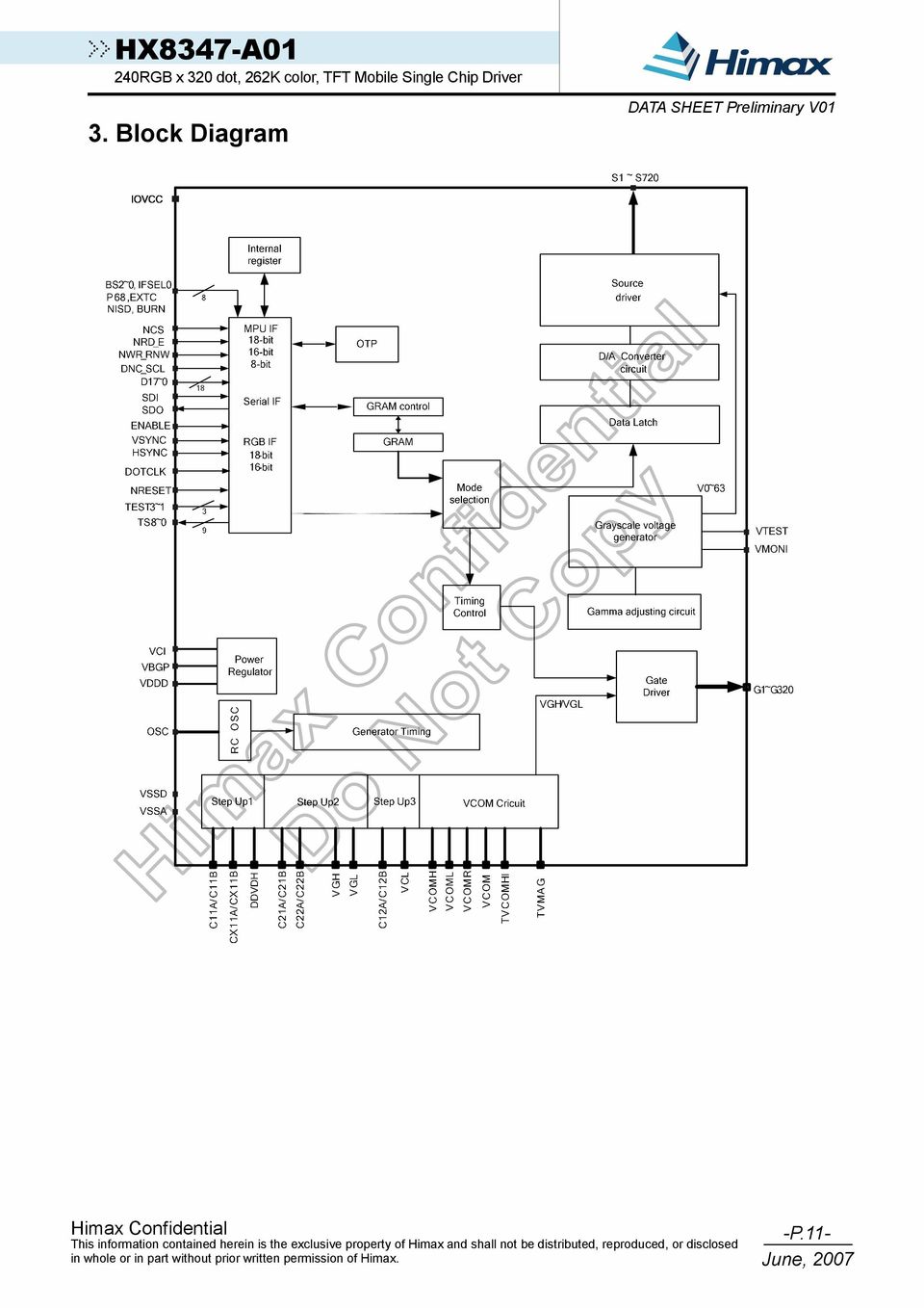
12 3. Block Diagram -P.11-
13 4. Pin Description 4.1 Pin Description Signals I/O Pin Number P68, BS2,BS1,BS0 I 4 Connected with VSSD/ IOVCC IFSEL0 I 1 MPU Input Parts Description Select the MPU interface mode as listed below Use with IFSEL0=1 Register-content interface mode P68 BS2 BS1 BS0 Interface mode DB pins bit bus interface, 80-system, 65K-Color 16-bit bus interface, 80-system, 262K-color 18-bit bus interface, 80-system, 262K-color 8-bit bus interface, 80-system, 262K-Color 16-bit bus interface, 80-system, 262K-Color 18-bit bus interface, 80-system, 262K-color 16-bit bus interface, 68-system, D17-D16 Unused, D15-D0 Data D17-D16 Unused, D15-D0 Data D17-D0 Data D17-D8 Unused D7-D0 Data D17-D8 Unused D7-D0 Data D17-D0 Data D17-D16 Unused, 65K-Color D15-D0 Data bit bus interface, 68-system, D17-D16 Unused, 262K-color D15-D0 Data bit bus interface, 68-system, D17-D0 Data 262K-Color bit bus interface, 68-system, D17-D8Unused 262K-color D7-D0 Data bit bus interface, 68-system, D17-D8 Unused 262K-Color D7-D0 Data bit bus interface, 68-system, D17-D0 Data 262K-color X 1 1 ID Serial bus IF DNC_SCL, SDO,SDI Interface format select pin IFSEL0 Interface Format Selection 0 Command-Parameter interface mode 1 Register-content interface mode In this case, the IFSEL0 has to be connected to IOVCC. EXTC I 1 MPU When operate in Register-content interface mode, the EXTC has to be connected to IOVCC or VSSD. NCS I 1 MPU Chip select signal. Low chip can be accessed; High chip cannot be accessed. Must be connected to VSSD if not in use. NWR_RNW I 1 MPU I80 system Serves as a write signal and writes data at the rising edge. M68 system 0 Write, 1 Read. Fix it to IOVCC or VSSD level when using serial buss interface. NRD_E I 1 MPU I80 system Serves as a read signal and read data at the low level. M68 system 0 Read/Write disable, 1 Read/Write enable. Fix it to IOVCC or VSSD level when using serial buss interface. BURN I 1 MPU Free Running mode If BURN=Hi, this can enable free running mode for burn in test. The display data alternates between full black and full white independent of input data in free running mode. SDI I 1 MPU Serial data input pin. If not used, please let it connected to IOVCC or VSSD. The signal for command or parameter select under parallel mode(i.e. Not serial interface) DNC_SCL I 1 MPU Low command. High parameter. When under serial interface, it servers as SCL. VSYNC I 1 MPU Frame synchronizing signal. Has to be fixed to IOVCC level if is not used. HSYNC I 1 MPU Frame synchronizing signal. Has to be fixed to IOVCC level if is not used. -P.12-

14 Signals I/O Pin Number Connected with Input Parts Description ENABLE I 1 MPU A data ENABLE signal in RGB I/F mode. Has to be fixed to VSSD level if unused (High active, if EPL=0). DOTCLK I 1 MPU Dot clock signal. Has to be fixed to VSSD level if is not used. NRESET I 1 MPU or reset Reset pin. Setting either pin low initializes the LSI. Must be reset after OSC I 1 VCOMR I 1 VGS I 1 circuit Oscillation Resistor Resistor or open VSSD or external resistor power is supplied. Oscillator input for test purpose. If not used, please let it open or connected to VSSD. A VcomH reference voltage. When adjusting VcomH externally, set registers to halt the VcomH internal adjusting circuit and place a variable resistor between VREG1 and VSSD. Otherwise, leave this pin open and adjust VcomH by setting the internal register of the HX8347-A. Connect to a variable resistor to adjusting internal gamma reference voltage for matching the characteristic of different panel used. Signals I/O Pin Number Connected with Output Part Description S1~S720 O 720 LCD Output voltages applied to the liquid crystal. G1~G320 O 320 LCD Gate driver output pins. These pins output VGH, VGL.(If not used, should be open) VCOM O 1 The power supply of common voltage in TFT driving. The voltage TFT common amplitude between VCOMH and VCOML is output. Connect this pin electrode to the common electrode in TFT panel. TE O 1 MPU Tearing effect output. If not used, please open this pin. SDO O 1 MPU Serial data output. If not use, let it to open. NISD O 1 Open Image Sticking Discharge signal. This pin is used for monitoring image sticking discharge phenomena. When the NISD goes low, the VGL, Source and VCOM would be discharged to VSSA. When the NISD goes high, the VGL, Source and VCOM are normal operation. -P.13-

15 Signals C11A,C11B C12A,C12B I/O Pin Number I/O 4 CX11A, CX11B I/O 2 C21A,C21B C22A,C22B I/O 4 Input/Output Part Connected with Step-up Capacitor Step-up Capacitor Step-up Capacitor D17~0 I/O 18 MPU Signals I/O Pin Number Connected with Description Connect to the step-up capacitors according to the step-up factor. Leave this pin open if the internal step-up circuit is not used. Connect to the step-up capacitors for step up circuit 1 operation. Leave this pin open if the internal step-up circuit is not used. Connect these pins to the capacitors for the step-up circuit 2. According to the step-up rate. When not using the step-up circuit2, disconnect them bit bi-directional data bus for system interface. 8-bit bus use D7-D0 and D17-D8 unused. 16-bit bus use D15-D0 and D17-D16 unused. 18-bit bus use D17-D bit data bus for RGB interface 16-bit bus use D15-D0 and D17-D16 unused. 18-bit bus use D17-D0 Connected unused pins to the VSSD level. Notice When register RGB_EN=1 and pin ENABLE=1, D[170] is used as stream image data for display. It means MPU data bus and RGB data bus is shared. Power Part Description IOVCC P 1 Power Supply Digital IO Pad power supply VCI P 1 Power Supply Analog power supply VSSD P 1 Ground Digital ground VSSA P 1 Ground Analog ground Stabilizing Output from internal logic voltage (1.6V). Connect to a stabilizing VDDD O 1 Capacitor capacitor If REGVDD = high, the internal VDDD regulator will be turned on. If REGVDD I 1 MPU REGVDD = low, the internal VDDD regulator will be turned off, VDDD should connect to external power supply, the VDDD voltage range is 1.65~1.95V. The REGVDD pin must be connected to IOVCC or VSSD. VBGP - 1 Open Band Gap Voltage. Let it to be open. Stabilizing VREG1 P 1 Capacitor Internal generated stable power for source driver unit. Stabilizing VREG3 P 1 Capacitor A reference voltage for VGH&VGL. VCOMH P 1 VCOML P 1 VCL P 1 DDVDH P 1 VGH P 1 VGL P 1 Stabilizing capacitor Stabilizing capacitor Stabilizing capacitor Stabilizing capacitor Stabilizing capacitor Stabilizing capacitor Connect this pin to the capacitor for stabilization. This pin indicates a high level of VCOM amplitude generated in driving the VCOM alternation. When the VCOM alternation is driven, this pin indicates a low level of VCOM amplitude. Connect this pin to a capacitor for stabilization. A negative voltage for VCOML circuit, VCL=-VCI An output from the step-up circuit1. Connect to a stabilizing capacitor between VSSA and DDVDH. Place a schotkey barrier diode (see configuration of the power supply ).DDVDH =4.5 to 5.5V An output from the step-up circuit2.or 4 ~ 6 time the VCI level. The step-up rate is determined with BT3-0 bits. Connect to a stabilizing capacitor between VSSD and VGH. Place a schottkey barrier diode between VCI and VGH. Place a schottkey barrier diode (see configuration of the power supply ).VGH=16.5V An output from the step-up circuit2.or 3 ~ -5 time the VCI level. The step-up rate is determined with BT3-0 bits. Connect to a stabilizing capacitor between VSSD and VGL. Place a schottkey barrier diode between VSSD and VGL. Place a schottkey barrier diode (see configuration of the power supply ).VGL=min -13.5V -P.14-

16 Test pin and others Signals I/O Pin Connected Number with Description TEST3-1 I 3 GND Test pin input (Internal pull low) TS8~0 O 9 Open A test pin. Disconnect it. VMONI O 1 Open A test pin. Disconnect it. VTEST O 1 Open Gamma voltage of Panel test pin output. Must be left open. TVCOMHI O 1 Open A test pin output. Must be left open. TVMAG O 1 Open A test pin output. Must be left open. DUMMYR Open Dummy pads. Available for measuring the COG contact resistance. DUMMYR14 and DUMMYR15 are short-circuited within the chip. DUMMY1-13 DUMMY Open Dummy pads IOGNDDUM O 1 Open Short-circuited within the chip -P.15-

17 4.2 Pin Assignment -P.16-

18 4.3 PAD Coordinates No. Pad name X Y No. Pad name X Y No. Pad name X Y No. Pad name X Y 1 DUMMY TS VCOML C11A TEST TS VCOML C11A IOGNDDUM TS VCOML C11A OSC TS VCOML C11A P TS VREG VGL EXTC REGVDD VREG VGL BS IOVCC VREG VGL BS IOVCC TVCOMHI VGL BS IOVCC VCOMR VGL IFSEL IOVCC TMAG VGL TEST IOVCC VCL VGL DUMMY IOVCC VCL VGL DUMMY VCI VCL VGL DUMMY VCI VCL VGL DUMMY VCI VCL VSSA DUMMY VCI DDVDH VSSA DUMMY VCI DDVDH VSSA DUMMY VCI DDVDH VGH NRESET VCI DDVDH VGH NRESET VCI DDVDH VGH VSYNC VCI DDVDH VGH HSYNC VCI VREG VGH DOTCLK VCI VREG VGH ENABLE VBGP VREG DUMMY D VSSA VDDD DUMMY D VSSA VDDD C12B D VSSA VDDD C12B D VSSA VDDD C12B D VSSA VDDD C12B DUMMY VSSA VDDD C12A D VSSA VDDD C12A D VSSA VDDD C12A D VGS VDDD C12A D VGS VDDD C21B D VSSD VDDD C21B TEST VSSD VDDD C21B DUMMY VSSD VDDD C21B D VSSD VDDD C21B D VSSD VDDD C21B D VSSD VDDD C21B D VSSD VDDD C21A D VSSD VDDD C21A D VSSD DUMMYR C21A D VSSD DUMMYR C21A D VMONI CX11B C21A DUMMY VTEST CX11B C21A SDO DUMMY CX11B C21A SDI VCOM CX11B C22B NRD_E VCOM CX11B C22B NWR_RNW VCOM CX11A C22B DNC_SCL VCOM CX11A C22B NCS VCOM CX11A C22B NISD VCOM CX11A C22B BURN VCOM CX11A C22B TE VCOMH C11B C22A DUMMY VCOMH C11B C22A TS VCOMH C11B C22A TS VCOMH C11B C22A TS VCOMH C11B C22A TS VCOMH C11A C22A P.17-

19 No. Pad name X Y No. Pad name X Y No. Pad name X Y No. Pad name X Y 241 C22A G G S DUMMY G G S DUMMY G G S DUMMY G G S G G G S G G G S G G G S G G G S G G G S G G G S G G G S G G G S G G G S G G G S G G G S G G G S G G G S G G G S G G G S G G G S G G G S G G G S G G G S G G G S G G G S G G G S G G G S G G G S G G G S G G G S G G G S G G G S G G G S G G G S G G G S G G G S G G G S G G G S G G G S G G G S G G G S G G G S G G G S G G G S G G DUMMY S G G DUMMY S G G S S G G S S G G S S G G S S G G S S G G S S G G S S G G S S G G S S G G S S G G S S G G S S G G S S G G S S P.18-

20 No. Pad name X Y No. Pad name X Y No. Pad name X Y No. Pad name X Y 481 S S S S S S S S S S S S S S S S S S S S S S S S S S S S S S S S S S S S S S S S S S S S S S S S S S S S S S S S S S S S S S S S S S S S S S S S S S S S S S S S S S S S S S S S S S S S S S S S S S S S S S S S S S S S S S S S S S S S S S S S S S S S S S S S S S S S S S S S S S S S S S S S S S S S S S S S S S S S S S S S S S S S S S S S S S S S S S S S S S S S S S S S S S S S S S S S S S S S S S S S S S S S S S S S S S S S S S S S S S S S S S S S S S S S S S S S S S S S S S S S P.19-

21 No. Pad name X Y No. Pad name X Y No. Pad name X Y No. Pad name X Y 721 S S S S S S S S S S S S S S S S S S S S S S S S S S S S S S S S S S S S S S S S S S S S S S S S S S S S S S S S S S S S S S S S S S S S S S S S S S S S S S S S S S S S S S S S S S S S S S S S S S S S S S S S S S S S S S S S S S S S S S S S S S S S S S S S S S S S S S S S S S S S S S S S S S S S S S S S S S S S S S S S S S S S S S S S S S S S S S S S S S S S S S S S DUMMY S S S DUMMY S S S S S S S S S S S S S S S S S S S S S S S S S S S S S S S S S S S S S S S S S S S S S S S S S S S P.20-
22 No. Pad name X Y No. Pad name X Y No. Pad name X Y No. Pad name X Y 961 S S S G S S S G S S S G S S S G S S S G S S S G S S S G S S S G S S S G S S S G S S S G S S S G S S S G S S S G S S S G S S S G S S S G S S S G S S S G S S S G S S S G S S S G S S S G S S S G S S S G S S S G S S S G S S S G S S S G S S S G S S S G S S S G S S S G S S S G S S S G S S S G S S S G S S S G S S S G S S S G S S S G S S S G S S S G S S S G S S S G S S S G S S S G S S S G S S DUMMY G S S DUMMY G S S G G S S G G S S G G S S G G S S G G S S G G S S G G S S G G S S G G S S G G P.21-
23 No. Pad name X Y No. Pad name X Y 1201 G G G G G G G G G G G G G G G G G G G G G G G G G G G G G G G G G G G G G G G G G G G G G G G G G G G G G G G G G G G G G DUMMY G G G Alignment mark X Y 1235 G A G A G G G G G G G G G G G G G G G G G G G G G G G G P.22-
24 4.4 Alignment Mark A_MARK (A1) A_MARK (A2) -P.23-
25 4.5 Bump Size Input PAD Output PAD -P.24-
26 5. Function Description 5.1 Interface Control Mode The HX8347-A supports three-type interface mode Command-Parameter interface mode, Register-Content interface mode, and RGB interface mode Command-Parameter interface mode or Register-Content interface mode is active by the external pins IFSEL0. RGB interface mode is active by internal bit RGB_EN setting as shown in Table5.1. There are two-type chip access formats in HX8347-A. One is register command for chip internal operation; the other is display data for chip display. REG_EN is stored in OTP for user application. IFSEL0 RGB_EN Register Data Display Data Command-parameter interface 0 0 From SRAM (Parallel interface) Command-parameter interface Sleep out Normal Display On From RGB interface 0 1 (Serial interface) Sleep out Partial Mode On From SRAM Register-content interface 1 0 From SRAM (Parallel interface) Register-content interface Normal display From RGB interface 1 1 (Serial interface) Partial Mode From SRAM Table 5. 1 Interface Mode Selection There are two-type register groups in HX8347-A. One is accessed only via Command-Parameter interface. The other is accessed only via Register-Content interface. This manual description focuses on Register-Content interface mode and RGB interface mode, about the Command-Parameter interface mode, please refer to the HX8347-A(N) datasheet for detail. -P.25-
27 5.1.1 Register-Content Interface Mode The register-content interface circuit in HX8347-A supports 18-/16-/8-bit bus width parallel bus system interface for I80 series and M68 series CPU, and serial bus system interface for serial data input. When NCS = L, the parallel and serial bus system interface of the HX8347-A become active and data transfer through the interface circuit is available. The DNC_SCL pin specifies whether the system interface circuit access is to the register command or to the GRAM. The input bus width format of system interface circuit is selected by external pins BS (2-0) setting. For selecting the input bus format, please refer to Table5.7 and Table5.8. In Register-Content interface, it includes an Index Register (IR) to store index data of internal control register and GRAM. Therefore, the IR can be written with the index pointer of the control register through data bus by setting DNC_SCL=0. Then the command or GRAM data can be written to register at which that index pointer pointed by setting DNC_SCL=1. Furthermore, there are two 18-bit bus control registers used to temporarily store the data written to or read from the GRAM. When the data is written into the GRAM from the MPU, it is first written into the write-data latch and then automatically written into the GRAM by internal operation. Data is read through the read-data latch when reading from the GRAM. Therefore, the first read data operation is invalid and the following read data operations are valid. P68 Input Signal Format Selection 0 Format for I80 series MPU 1 Format for M68 series MPU Table 5. 2 MPU Selection in Command-Parameter Interface Circuit BS2 BS1 BS0 Interface Transferring Method of GRAM data bit system interface 16-bit 65K-color bit system interface 18-bit 262K-color (16+2) bit system interface 18-bit 262K-color bit system interface 18-bit 262K-color (6+6+6) bit system interface 18-bit 262K-color (16+2) bit system interface 18-bit 262K-color 1 1 ID Serial interface Select by register 3Ah Table 5. 3 Interface Selection in Register-Content Interface Mode Transferring Method of Command 8-bit collective -P.26-
28 Parallel Bus System Interface The input / output data from data pins (D17-0) and signal operation of the I80/M68 series parallel bus interface are listed in Table 5.9 and Table Operations E_NWR RW_NRD DNC_SCL Writes Indexes into IR Reads internal status Writes command into register or data into GRAM Reads command from register or data from GRAM Table 5. 4 Data Pin Function for I80 Series CPU Operations E_NWR RW_NRD DNC_SCL Writes Indexes into IR Reads internal status Writes command into register or data into GRAM Reads command from register or data from GRAM Table 5. 5 Data Pin Function for M68 Series CPU Write to the register NCS DNC_SCL NRD_E NWR_RNW D7-0 "index" write to index register Command write to the register Read the register NCS DNC_SCL NRD_E NWR_RNW D7-0 "index" write to index register Command read from the register Figure 5. 1 Register Read/Write Timing in Parallel Bus System Interface (for I80 Series MPU) -P.27-
29 NCS DNC_SCL NRD_E NWR_RNW D15-0/ D17-0 "22"h write to index register Display data write to RAM Display data write to RAM nth pixel, Address = N (n+1) pixel, Address = N +1 NCS DNC_SCL NRD_E NWR_RNW D7-0 "22" h 1st write data 2nd write data 1 st write data 2 nd write data nth pixel ; Address = N (n+1)th pixel ; Address = N+1 (n+1)th pixel ; Address = N+2 NCS DNC_SCL NRD_E NWR_RNW D17-0 "22"h dummy read data 1st read data 1 pixel data (The format refer 18-bit Interface) NCS DNC_SCL NRD_E NWR_RNW 1st read data 2nd read read 3rd read data D7-0 "22" h R G B R G Dummy Read Data 1 pixel data (The format refer 8-bit Interface) Figure 5. 2 GRAM Read/Write Timing in 16-/18-Bit Parallel Bus System Interface (for I80 Series MPU) -P.28-
30 Write to the graphic RAM (8-bit 262K Color) NCS DNC_SCL NRD_E NWR_RNW D7-0 "22" h 1st write data 2nd write data 3rd write data 1st write data 2nd write data 3rd write data nth pixel ; Address = N (n+1)th pixel ; Address = N+1 Read the graphic RAM (8-bit 262K Color) NCS DNC_SCL NRD_E NWR_RNW 1st read data 2nd read read 3rd read data D7-0 "22" h R G B R G Dummy Read Data 1 pixel data (The format refer 8-bit Interface) Figure 5. 3 GRAM Read/Write Timing in 8-Bit Parallel Bus System Interface (for I80 Series MPU) -P.29-
31 Write to the register NCS DNC_SCL NWR_RNW NRD_E D7-0 "index" write to index register Command write to the register Read the register NCS DNC_SCL NWR_RNW NRD_E D7-0 "index" write to index register Command read from the register Figure 5. 4 Register Read/Write Timing in Parallel Bus System Interface (for M68 Series MPU) -P.30-
32 NCS DNC_SCL NWR_RNW NRD_E D15-0/ D17-0 "22"h write to index register Display data write to RAM Display data write to RAM nth pixel, Address = N (n+1) pixel, Address = N +1 NCS DNC_SCL NWR_RNW NRD_E D15-0 "22" h 1st write data 2nd write data 1st write data 2nd write data 1st write data 2nd write data nth pixel ; Address = N (n+1)th pixel ; Address = N+1 (n+2)th pixel ; Address = N+2 NCS DNC_SCL NWR_RNW NRD_E D17-0 "22"h dummy read data 1st read data 1 pixel data (The format refer 18-bit Interface) NCS DNC_SCL NWR_RNW NRD_E D7-0 "22" h 1st read data 2nd read data 3rd read data R G B R G Dummy Read Data 1 pixel data (The format refer 8-bit Interface) Figure 5. 5 GRAM Read/Write Timing in 16-/18-Bit Parallel Bus System Interface (for M68 Series MPU) -P.31-
33 NCS DNC_SCL NWR_RNW NRD_E D7-0 "22" h 1st write data 2nd write data 3rd write data 1st write data 2nd write data 3rd write data nth pixel ; Address = N (n+1)th pixel ; Address = N+1 NCS DNC_SCL NWR_RNW NRD_E D7-0 "22" h 1st read data 2nd read data 3rd read data R G B R G Dummy Read Data 1 pixel data (The format refer 8-bit Interface) Figure 5. 6 GRAM Read/Write Timing in 8-bit Parallel Bus System Interface (for M68 Series MPU) -P.32-
34 18-bit Parallel Bus System Interface The I80-system 18-bit parallel bus interface in command-parameter interface mode can be used by setting external pins P68, BS2, BS1, BS0 pins to 0010 or And the M68-system 18-bit parallel bus interface in command-parameter interface mode can be used by setting P68, BS2, BS1, BS0 pins to 1010 or Figure 5.8 is the example of interface with I80/M68 microcomputer system interface. Figure 5. 7 Example of I80- / M68- System 16-Bit Parallel Bus Interface Transfer Order 1 18-bit Data Input Data Bus D 17 D 16 D 15 D 14 D 13 D 12 D 11 D 10 D 9 D 8 D 7 D 6 D 5 D 4 D 3 D 2 D 1 D 0 GRAM Data R 5 R 4 R 3 R 2 R 1 R 0 G 5 G 4 G 3 G 2 G 1 G 0 B5 B4 B3 B2 B1 B0 262,144 Colors are avaliable Figure 5. 8 Input Data Bus and GRAM Data Mapping in 18-Bit Bus System Interface ( BS2, BS1, BS0 = 010 or 101 ) -P.33-
35 16-bit Parallel Bus System Interface The I80-system 16-bit parallel bus interface in command-parameter interface mode can be used by setting external pins P68, BS2, BS1, BS0 pins to 0000, 0001, And the M68-system 16-bit parallel bus interface in command-parameter interface mode can be used by setting P68, BS2, BS1, BS0 pins to 1000, 1001, Figure 5.10 is the example of interface with I80/M68 microcomputer system interface. Figure 5. 9 Example of I80- / M68- System 16-bit Parallel Bus Interface Figure Input Data Bus and GRAM Data Mapping in 16-Bit Bus System Interface with 16 Bit-Data Input ( BS2, BS1, BS0 = 000 ) Figure Input Data Bus and GRAM Data Mapping in 16-Bit Bus System Interface with 18(16+2) Bit-Data Input ( BS2, BS1, BS0 = 001 ) -P.34-
36 Figure Input Data Bus and GRAM Data Mapping in 16-Bit Bus System Interface with 18(6+6+6) Bit-Data Input ( BS2, BS1, BS0 = 100 ) 8-bit Parallel Bus System Interface The I80-system 8-bit parallel bus interface in register-content interface mode can be used by setting external pins P68, BS2, BS1, BS0 pins to And the M68-system 8-bit parallel bus interface in command-parameter interface mode can be used by setting P68, BS2, BS1, BS0 pins to Figure 5.14 is the example of interface with I80/M68 microcomputer system interface. Figure Example of I80- / M68- System 8-Bit Parallel Bus Interface Figure Input Data Bus and GRAM Data Mapping in 8-Bit Bus System Interface with 18( ) Bit-Data Input ( BS2, BS1, BS0 = 011 ) -P.35-
37 5.1.2 Serial Bus System Interface The HX8347-A supports the serial bus interface in register-content mode by setting external pins BS2, BS1 pins to 11. The serial bus system interface mode is enabled through the chip select line (NCS), and it is accessed via a control consisting of the serial input data (SDI), serial output data (SDO) and the serial transfer clock signal (DNC_SCL). As the chip select signal (NCS) goes low, the start byte needs to be transferred first. The start byte is made up of 6-bit bus device identification code, register select (RS) bit and read/write operation (RW) bit. The five upper bits of 6-bit bus device identification code must be set to 01110, and the least significant bit of the identification code must be set as the external pin BS0 input as ID. The seventh bit (RS) of the start byte determines internal index register or register, GRAM accessing. RS must be set to 0 when writing data to the index register or reading the status, and it must be set to 1 when writing or reading an command or GRAM data. The read or write operation is selected by the eighth bit (RW) of the start byte. The data is written to the chip when R/W = 0, and read from chip when RW = 1. RS R/W Function 0 0 Writes Indexes into IR 1 0 Writes internal status and GRAM 1 1 Reads command into register or data into GRAM Table 5. 6 The Function of RS and R/W Bit bus -P.36-
38 Figure Data Write Timing in Serial Bus System Interface -P.37-
39 A)TransferTiming Format in Serial Bus Interface for Register Read DNC_SCL (Input) NCS Start End SDI (Input) "01110" ID Device ID code Start byte RS RW Status read, register read SDO (Output) D7 D6 D5 D4 D3 D2 D1 D0 Status read, register read Figure Data Read Timing in Serial Bus System Interface -P.38-
40 5.1.3 RGB Interface The HX8347-A supports the RGB interface for writing animated display data. The RGB interface can be selected by setting internal RGB_EN bit = 1. In RGB interface, the display operations is executed in synchronization with the frame synchronizing signal (VSYNC), line synchronizing signal (HSYNC) and dot clock (DOTCLK), and the display data is inputted via RGB interface circuit without being written to the GRAM and display directly. The display data are transferred in pixel unit via D17-0 input pins. The display data input is latched on the rising edge of DOTCLK (DPL bit = 0) or the falling edge of DOTCLK (DPL bit = 1) by the chip when ENABLE signal is valid. Please refer to Table EPL ENABLE Display Data to Panel 0 0 Enable 0 1 Disable 1 0 Disable 1 1 Enable Table 5. 7 EPL Bit Setting and Valid Enable Signal (VSPL bit=0) VSYNC Vertical Back porch Display data to Panel Display period Horizontal Back porch HSYNC DOTCLK ENABLE ( HSPL bit = 0 ) ( DPL bit = 0 ) ( EPL bit = 0 ) D17-0 Figure RGB Interface Circuit Input Timing -P.39-
41 There are two types bit format per pixel color order for writing GRAM data in 18-bit bus interface selected by internal bits CSEL(2-0). The setting is shown in Figure5. 19 and Figure (1) 16 bit/pixel color order (R 5-bit, G 6-bit, B 5-bit), 65,536 colors (CSEL(2-0) = 101 ) NRESET VSYNC HSYNC ENABLE DOTCLK D17 D16 D15 D14 D13 R14 R24 R34 R44 R54 R13 R23 R33 R43 R53 R12 R22 R32 R42 R52 R11 R21 R31 R41 R51 R10 R20 R30 R40 R50 D12 D11 D10 D9 D8 D7 D6 D5 D4 D3 D2 D1 G15 G25 G35 G45 G55 G14 G24 G34 G44 G54 G13 G23 G33 G43 G53 G12 G22 G32 G42 G52 G11 G21 G31 G41 G51 G10 G20 G30 G40 G50 B14 B24 B34 B44 B54 B13 B23 B33 B43 B53 B12 B22 B32 B42 B52 B11 B21 B31 B41 B51 B10 B20 B30 B40 B50 D0 16-bit (Pixel n) 16-bit (Pixel n+1) 16 -bit (Pixel n+2) (bit extension) Rlsb = Rmsb, Blsb=Bmsb, don t need lookup table 18-bit/pixel R 1 G 1 B1 R 2 G 2 B2 R 3 G 3 B3 Figure Bit / Pixel Data Input of RGB Interface -P.40-
42 (2) 18 bit/pixel color order (R 6-bit, G 6-bit, B 6-bit), 262,144 colors (CSEL(2-0) = 110 ) NRESET VSYNC HSYNC ENABLE DOTCLK D17 D16 D15 D14 D13 D12 D11 D10 D9 D8 D7 D6 D5 D4 D3 D2 D1 R15 R25 R35 R45 R55 R14 R24 R34 R44 R54 R13 R23 R33 R43 R53 R12 R22 R32 R42 R52 R11 R21 R31 R41 R51 R10 R20 R30 R40 R50 G15 G25 G35 G45 G55 G14 G24 G34 G44 G54 G13 G23 G33 G43 G53 G12 G22 G32 G42 G52 G11 G21 G31 G41 G51 G10 G20 G30 G40 G50 B15 B25 B35 B45 B55 B14 B24 B34 B44 B54 B13 B23 B33 B43 B53 B12 B22 B32 B42 B52 B11 B21 B31 B41 B51 D0 B10 B20 B30 B40 B50 18-bit (Pixel n) 18-bit (Pixel n+1) 18-bit (Pixel n+2) R 1 G 1 B1 R 2 G 2 B2 R 3 G 3 B3 Figure Bit / Pixel Data Input of RGB Interface -P.41-
43 5.2 Address Counter (AC) The HX8347-A contains an address counter (AC) which assigns address for writing/reading pixel data to/from GRAM. The address pointers set the position of GRAM whose addresses range X=0~239d and Y=0~319d. Every time when a pixel data is written into the GRAM, the X address or Y address of AC will be automatically increased by 1 (or decreased by 1), which is decided by the register (MV, MX and MY bit) setting. To simplify the address control of GRAM access, the window address function allows for writing data only to a window area of GRAM specified by registers. After data is written to the GRAM, the AC will be increased or decreased within setting window address-range which is specified by the horizontal address register (start SC, end EC) or the vertical address register (start SP, end EP). Therefore, the data can be written consecutively without thinking a data wrap by those bit function. -P.42-
44 5.2.1 MCU to Memory Write/Read Direction B Data stream from MCU is like this figure E Figure MCU to Memory Write/Read Direction The data is written in the order as illustrated above. The counter that dictates which physical memory the data is to be written is controlled by Memory Access Control Command, Bits MY, MX, MV as described below. Figure MY, MX, MV Setting MY MX MV CASET PASET Direct to Physical Column Pointer Direct to Physical Page Pointer Direct to Physical Column Pointer Direct to (319-Physical Page Pointer) Direct to (239-Physical Column Pointer) Direct to Physical Page Pointer Direct to (239-Physical Column Pointer) Direct to (319-Physical Page Pointer) Direct to Physical Page Pointer Direct to Physical Column Pointer Direct to (319-Physical Page Pointer) Direct to Physical Column Pointer Direct to Physical Page Pointer Direct to (239-Physical Column Pointer) Direct to (319-Physical Page Pointer) Direct to (239-Physical Column Pointer) Table 5. 8 MY, MX, MV Setting -P.43-
45 The following figure depicts the update method set by MV, MX and MY bit. Display Data Direction MADCTR parameter MV MX MY Image in the Host Image in the Driver (GRAM) B H/W Position (0,0) B Normal X,Y address (0,0) X CASET Y RASET E E B H/W Position (0,0) E Y-Mirror E X,Y address (0,0) X CASET Y RASET B B X-Mirror E B X-Mirror Y-Mirror E B H/W Position (0,0) B X-Y Exchange X,Y address (0,0) X CASET Y RASET E E X-Y Exchange Y-Mirror B E H/W Position (0,0) X,Y address (0,0) X CASET Y RASET B E X-Y Exchange X-Mirror B E H/W Position (0,0) E B X,Y address (0,0) X CASET Y RASET X-Y Exchange X-Mirror Y-Mirror B E H/W Position (0,0) Figure Address Direction Settings E B X,Y address (0,0) X CASET Y RASET -P.44-
46 5.3 Source, Gate and Memory Map Pixel1 Pixel2 Pixel239 Pixel240 Source Out S1 S2 S3 S4 S5 S6 S715 S716 S717 S718 S719 S720 MY=0 RA R0 5-0 G0 5-0 B0 5-0 R1 5-0 G15-0 B R238 G238 B238 R239 G B MY= RGB Order BGR=0 BGR=1 -- Display Pattern Data RN 7-0 GN 7-0 BN MX= CA MX= Figure Memory Map (240RGBx320) NOTE RA = Row Address, CA = Column Address, MX = Mirror X-axis (Column address direction parameter), D6 parameter of Memory Access Control command MY = Mirror Y-axis (Row address direction parameter), D7 parameter of Memory Access Control command RGB= Red, Green and Blue pixel position change, D3 parameter of Memory Access Control command P.45-
47 5.4 Tearing Effect Output Line The Tearing Effect output line supplies to the MPU a Panel synchronization signal. This signal can be enabled or disabled by the Tearing Effect Line Off & On commands. The mode of the Tearing Effect signal is defined by the parameter of the Tearing Effect Line On command. The signal can be used by the MPU to synchronize Frame Memory Writing when displaying video images. Tearing effect function is not support when set DIM not equal Tearing Effect Line Modes Mode 1, the Tearing Effect Output signal consists of V-Blanking Information only Figure TE mode 1 output t VREG1= The LCD display is not updated from the Frame Memory t vdl = The LCD display is updated from the Frame Memory (except Invisible Line see below) Mode 2, the Tearing Effect Output signal consists of V-Blanking and H-Blanking Information, there is one V-sync and 320 H-sync pulses per field. t hdl t hdh V-Sync V-Sync Invisible Line 1st Line 2nd Line Figure TE mode 2 output 161th Line 162th Line t hdh= The LCD display is not updated from the Frame Memory t hdl= The LCD display is updated from the Frame Memory (except Invisible Line see above) Figure TE output waveform Note During Sleep In Mode, the Tearing Output Pin is active Low -P.46-
48 5.4.2 Tearing Effect Line Timing The Tearing Effect signal is described below. Figure Waveform of Tearing Effect Signal Idle Mode Off (Frame Rate = TBD Hz) Symbol Parameter Min. Max. Unit Description tvdl Vertical Timing Low Duration TBD - ms - tvdh Vertical Timing High Duration BP+FP - us - thdl Horizontal Timing Low Duration TBD - us - thdh Horizontal Timing High Duration TBD 500 us - Table 5. 9 AC characteristics of Tearing Effect Signal The signal s rise and fall times (tf, tr) are stipulated to be equal to or less than 15ns. Figure Timing of Tearing Effect Signal The Tearing Effect Output Line is fed back to the MPU and should be used as shown below to avoid Tearing Effect -P.47-
49 5.4.3 Example 1 MPU Write is faster than Panel Read MCU to Memory 1st 320th Time TE output signal Time Memory to LCD 1st 320th Image on LCD a b c d Time Figure Data write to Frame Memory is now synchronized to the Panel Scan. It should be written during the vertical sync pulse of the Tearing Effect Output Line. This ensures that data is always written ahead of the panel scan and each Panel Frame refresh has a complete new image Figure P.48-
50 5.4.4 Example 2 MPU Write is slower than Panel Read MCU to Memory 1st 320th Time TE output signal Time Memory to LCD 1st 320th Image on LCD a b c d e f Time Figure The MPU to Frame Memory write begins just after Panel Read has commenced i.e. after one horizontal sync pulse of the Tearing Effect Output Line. This allows time for the image to download behind the Panel Read pointer and finishing download during the subsequent Frame before the Read Pointer catches the MPU to Frame memory write position. Figure P.49-
51 5.5 Oscillator The HX8347-A has an internal oscillator without extra external components that provide a source for system clock generator. The default frequency is 5.5Mhz. 5.6 Source Driver The HX8347-A contains a 720 channels of source driver (S1~S720) which is used for driving the source line of TFT LCD panel. The source driver converts the digital data from GRAM into the analog voltage for 720 channels and generates corresponding gray scale voltage output, which can realize a 262K colors display simultaneously. Since the output circuit of this source driver incorporates an operational amplifier, a positive and a negative voltage can be alternately outputted from each channel. 5.7 Gate Driver The HX8347-A contains a 320 gate channels of gate driver (G1~G320) which is used for driving the gate. The gate driver level is VGH when scan some line, VGL the other lines. -P.50-
52 5.8 LCD Power Generation Circuit LCD Power Generation Scheme The boost voltage generated is shown as below. VGH VGH(4 VCI~6 VCI) x 4~6 DC/DC VCI (2.3 ~ 3.3V) x 2~3 DC/DC VLCD VREG1 VCOMH DDVDH (4.6V ~ 6.4V) VREG3 VREG1 (3.5 ~ (DDVDH-0.5)V) VCOMH IOVCC (1.65V~3.3V) VDDD VDDD(1.8V) VCOM Amplitude VBGP(1.25V) VSSA, VSSD (0V) DC/DC x (-1) VCOML VCL DC/DC x (-3)~(-5) VCOML VGL VGL(-5 VCI ~ -3 VCI) Figure LCD Power Generation Scheme -P.51-
53 5.8.2 Various Boosting Steps The boost steps of each boosting voltage are selected according to how the external capacitors are connected. Different booster applications are shown as below. DDVDH=2xVCI C11A DDVDH C11B C21A VGH=6xVCI VGL=-5xVCI VGH C21B C22A VGL C22B VCL=-1xVCI C12A VCL C12B Figure Various Boosting Steps -P.52-
54 5.9 Gray Voltage Generator for Source Driver The HX8347-A incorporates gamma adjustment function for the 262,144-color display (64 grayscale for each R, G, B color). Gamma adjustment operation is implemented by deciding the 8 grayscale levels firstly in gamma adjustment control registers to match the LCD panel. These registers are available for both polarities. Graphics RAM (GRAM) R 5 R 4 R 3 R 2 R R 1 0 GG G G GG B 5 B 4 B 3 B 2 B B bit Grayscale 6-bit Grayscale 6-bit Grayscale D/A Converter D/A Converter D/A Converter Output Driver Output Driver Output Driver R G B LCD V0 V1 V63 Grayscale Voltage Generator OP 04 OP 14 OP 13 Positive polarity Register ON 14 ON ON Negative polarity Registre OP 03 OP OP OP OP OP CP CP CP CP CP CP MP MP MP MP MP MP MP MP MP MP MP MP MP MP MP MP MP MP ON ON CN CN MN MN MN MN MN MN ON ON CN ON ON CN CN CN MN MN MN MN MN MN MN MN MN MN MN MN Figure Grayscale Control -P.53-
55 5.9.1 Structure of Grayscale Voltage Generator Eight reference gamma voltages VgP/N(0, 1, 8, 20, 43, 55, 62, 63) for positive and negative polarity are specified by the center adjustment, the micro adjustment and the offset adjustment registers firstly. With those eight voltage injected into specified node of grayscale voltage generator, totally 64 grayscale voltages (V0-V63) can be generated from grayscale amplifier for LCD panel. Figure Structure of Grayscale Voltage Generator -P.54-
56 5.9.2 Gamma-Characteristics Adjustment Register This HX8347-A has register groups for specifying a series grayscale voltage that meets the Gamma-characteristics for the LCD panel. These registers are divided into two groups, which correspond to the gradient, amplitude, and macro adjustment of the voltage for the grayscale characteristics. The polarity of each register can be specified independently. (R, G, and B are common.) Offset Adjustment Registers 0/1 The offset adjustment variable registers are used to adjust the amplitude of the grayscale voltage. This function is implemented by controlling these variable resisters in the top and bottom of the gamma resister stream for reference gamma voltage generation. These registers are available for both positive and negative polarities Gamma Center Adjustment Registers The gamma center adjustment registers are used to adjust the reference gamma voltage in the middle level of grayscale without changing the dynamic range. This function is implemented by choosing one input of 8 to 1 selector in the gamma resister stream for reference gamma voltage generation. These registers are available for both positive and negative polarities Gamma Macro Adjustment Registers The gamma macro adjustment registers can be used for fine adjustment of the reference gamma voltage. This function is implemented by controlling the 8-to-1 selectors (MP/N0~5), each of which has 8 inputs and generates one reference voltage output (Vg(P/N)1, 8, 20, 43, 55, 62). These registers are available for both positive and negative polarities. Register Positive Negative Groups Polarity Polarity Description Center CP0 2-0 CN0 2-0 Variable resistor (VRCP/N0) for center adjustment Adjustment CP1 2-0 CN1 2-0 Variable resistor (VRCP/N1)for center adjustment MP0 2-0 MN to-1 selector (voltage level of grayscale 1) Macro Adjustment MP1 2-0 MN to-1 selector (voltage level of grayscale 8) MP2 2-0 MN to-1 selector (voltage level of grayscale 20) MP3 2-0 MN to-1 selector (voltage level of grayscale 43) MP4 2-0 MN to-1 selector (voltage level of grayscale 55) MP5 2-0 MN to-1 selector (voltage level of grayscale 62) Offset OP0 3-0 ON0 3-0 Variable resistor (VROP/N0)for offset adjustment Adjustment OP1 4-0 ON1 4-0 Variable resistor (VROP/N1)for offset adjustment Table Gamma-Adjustment Registers -P.55-
57 5.9.4 Gamma Resister Stream and 8 to 1 Selector The block consists of two gamma resister streams, one is for positive polarity and the other is for negative polarity, each one includes eight gamma reference voltages (Vg(P/N)0, 1, 8, 20, 43, 55, 62, 63). Furthermore, the block has a pin (VGS) to connect a variable resistor outside the chip for the variation between panels, if needed. VREG1 CGMP0 CGMP1 VGS OP0 0-15R*2 50R 1R 5R 4R*7 1R*7 4R* R OP1 1R* R*7 1R*7 4R*7 50R 1R 5R 0-28R 5R 1R*7 16R 1R*7 5R 1R*7 0-28R VP0 VP1 VP2 VP3 VP4 VP5 VP6 VP7 VP8 VP9 VP10 VP11 VP12 VP13 VP14 VP15 VP16 VP17 VP18 VP19 VP20 VP21 VP22 VP23 VP24 VP25 VP26 VP27 VP28 VP29 VP30 VP31 VP32 VP33 VP34 VP35 VP36 VP37 VP38 VP39 VP40 VP41 VP42 VP43 VP44 VP45 VP46 VP47 VP48 VP49 VgP0 VgP1 Buffer Selector NP0 Center adjustment CP0 VgP2 Buffer Selector NP1 VgP3 Buffer Selector NP2 VgP4 Selector VgP5 Selector VgP6 VgP7 Buffer NP3 Buffer NP4 Center adjustment CP1 Buffer Selector NP R 3.733R 4.8R CGMP2=1 GSEL SEL 0 MUX 1 out 2.4R 2.4R 2.4R 2.4R 2.4R 2.4R 2.4R 2.4R 2.4R 2.4R CGMP3=1 2.4R 4.8R 2.4R 3.733R 2.4R 7.467R 2.4R 1 out MUX 0 sel GSEL R1 R2 R3 R4 R5 R6 R7 R8 2R R9 2R R19 2R R20 1R R21 1R R41 1R R42 1R R43 2R R44 2R R53 2R R54 2R R55 R56 R57 R58 R59 R60 R61 V0 V1 V2 V3 V4 V5 V6 V7 V8 V9 V10 V19 V20 V21 V22 V41 V42 V43 V44 V45 V54 V55 V56 V57 V58 V59 V60 V61 V62 V63 -P.56-
58 Figure Gamma Resister Stream and Gamma Reference Voltage -P.57-
59 5.9.5 Variable Resister There are two types of variable resistors, one is for center adjustment, the other is for offset adjustment. The resistances are decided by setting values in the center adjustment, offset adjustment registers. Their relationship is shown as below. Value in Register O(P/N)0 3-0 Resistance VRO(P/N)0 Value in Register O(P/N)1 4-0 Resistance VRO(P/N)1 Value in Register C(P/N)0/ R R 000 0R R R 001 4R R R 010 8R Resistance VRC(P/N) R R R R R R R R R R R Table Offset Adjustment 0 Table 5. 12Offset Adjustment 1 Table Center Adjustment 8 to 1 Selector The 8 to 1 selector has eight input voltages generated by gamma resister stream, and outputs one reference voltages selected from inputs for gamma reference voltage generation by setting value in macro adjustment register. There are six 8 to 1 selectors and the relationship is shown as below. Value in Register Voltage level M(P/N) 2-0 Vg(P/N) 1 M(P/N) 2-0 Vg(P/N) 1 M(P/N) 2-0 Vg(P/N) 1 M(P/N) VP(N)1 000 VP(N)1 000 VP(N) VP(N)2 001 VP(N)2 001 VP(N) VP(N)3 010 VP(N)3 010 VP(N) VP(N)4 011 VP(N)4 011 VP(N) VP(N)5 100 VP(N)5 100 VP(N) VP(N)6 101 VP(N)6 101 VP(N) VP(N)7 110 VP(N)7 110 VP(N) VP(N)8 111 VP(N)8 111 VP(N)8 111 Table Output Voltage of 8 to 1 Selector -P.58-
60 240RGB x 320 dot, 262K color, with internal GRAM, TFT Mobile Single Chip Driver The grayscale levels are determined by the following formulas Reference Voltage Macro Adjustment Value Formula VgP [(VREG1-VD*VROP0 /SumRP)] *GSEL +VREG1-(VREG1*GSEL) VP0 NP0 2-0=000 VREG1-VD[(VROP0+(CGMP0*1R)+5R- (CGMP0*5R)] /SumRP VP1 NP0 2-0=001 VREG1-VD[(VROP0+(CGMP0*2R)+9R- (CGMP0*9R)] /SumRP VP2 NP0 2-0=010 VREG1-VD[(VROP0+(CGMP0*3R)+13R- (CGMP0*13R)] /SumRP VP3 VgP1 NP0 2-0=011 VREG1-VD[(VROP0+(CGMP0*4R)+17R- (CGMP0*17R)] /SumRP VP4 NP0 2-0=100 VREG1-VD[(VROP0+(CGMP0*5R)+21R- (CGMP0*21R)] /SumRP VP5 NP0 2-0=101 VREG1-VD[(VROP0+(CGMP0*6R)+25R- (CGMP0*25R)] /SumRP VP6 NP0 2-0=110 VREG1-VD[(VROP0+(CGMP0*7R)+29R- (CGMP0*29R)] /SumRP VP7 NP0 2-0=111 VREG1-VD[(VROP0+(CGMP0*8R)+33R- (CGMP0*33R)] /SumRP VP8 NP1 2-0=000 VREG1-VD[(VROP0+(CGMP0*8R)+33R- (CGMP0*33R) +VRCP0] /SumRP VP9 NP1 2-0=001 VREG1-VD[(VROP0+(CGMP0*9R)+34R- (CGMP0*34R) +VRCP0] /SumRP VP10 NP1 2-0=010 VREG1-VD[(VROP0+(CGMP0*10R)+35R- (CGMP0*35R) +VRCP0] /SumRP VP11 VgP2 NP1 2-0=011 VREG1-VD[(VROP0+(CGMP0*11R)+36R- (CGMP0*36R) +VRCP0] /SumRP VP12 NP1 2-0=100 VREG1-VD[(VROP0+(CGMP0*12R)+37R- (CGMP0*37R) +VRCP0] /SumRP VP13 NP1 2-0=101 VREG1-VD[(VROP0+(CGMP0*13R)+38R- (CGMP0*38R) +VRCP0] /SumRP VP14 NP1 2-0=110 VREG1-VD[(VROP0+(CGMP0*14R)+39R- (CGMP0*39R) +VRCP0] /SumRP VP15 NP1 2-0=111 VREG1-VD[(VROP0+(CGMP0*15R)+40R- (CGMP0*40R) +VRCP0] /SumRP VP16 NP2 2-0=000 VREG1-VD[(VROP0+(CGMP0*20R)+45R- (CGMP0*45R) +VRCP0] /SumRP VP17 NP2 2-0=001 VREG1-VD[(VROP0+(CGMP0*21R)+46R- (CGMP0*46R) +VRCP0] /SumRP VP18 NP2 2-0=010 VREG1-VD[(VROP0+(CGMP0*22R)+47R- (CGMP0*47R) +VRCP0] /SumRP VP19 VgP3 NP2 2-0=011 VREG1-VD[(VROP0+(CGMP0*23R)+48R- (CGMP0*48R) +VRCP0] /SumRP VP20 NP2 2-0=100 VREG1-VD[(VROP0+(CGMP0*24R)+49R- (CGMP0*49R) +VRCP0] /SumRP VP21 NP2 2-0=101 VREG1-VD[(VROP0+(CGMP0*25R)+50R- (CGMP0*50R) +VRCP0] /SumRP VP22 NP2 2-0=110 VREG1-VD[(VROP0+(CGMP0*26R)+51R- (CGMP0*51R) +VRCP0] /SumRP VP23 NP2 2-0=111 VREG1-VD[(VROP0+(CGMP0*27R)+52R- (CGMP0*52R) +VRCP0] /SumRP VP24 NP3 2-0=000 VREG1-VD[(VROP0+(CGMP0*43R)+68R- (CGMP0*68R) +VRCP0] /SumRP VP25 NP3 2-0=001 VREG1-VD[(VROP0+(CGMP0*44R)+69R- (CGMP0*69R) +VRCP0] /SumRP VP26 NP3 2-0=010 VREG1-VD[(VROP0+(CGMP0*45R)+70R- (CGMP0*70R) +VRCP0] /SumRP VP27 VgP4 NP3 2-0=011 VREG1-VD[(VROP0+(CGMP0*46R)+71R- (CGMP0*71R) +VRCP0] /SumRP VP28 NP3 2-0=100 VREG1-VD[(VROP0+(CGMP0*47R)+72R- (CGMP0*72R) +VRCP0] /SumRP VP29 NP3 2-0=101 VREG1-VD[(VROP0+(CGMP0*48R)+73R- (CGMP0*73R) +VRCP0] /SumRP VP30 NP3 2-0=110 VREG1-VD[(VROP0+(CGMP0*49R)+74R- (CGMP0*74R) +VRCP0] /SumRP VP31 NP3 2-0=111 VREG1-VD[(VROP0+(CGMP0*50R)+75R- (CGMP0*75R) +VRCP0] /SumRP VP32 NP4 2-0=000 VREG1-VD[(VROP0+(CGMP0*55R)+80R- (CGMP0*80R) +VRCP0] /SumRP VP33 NP4 2-0=001 VREG1-VD[(VROP0+(CGMP0*56R)+81R- (CGMP0*81R) +VRCP0] /SumRP VP34 NP4 2-0=010 VREG1-VD[(VROP0+(CGMP0*57R)+82R- (CGMP0*82R) +VRCP0] /SumRP VP35 VgP5 NP4 2-0=011 VREG1-VD[(VROP0+(CGMP0*58R)+83R- (CGMP0*83R) +VRCP0] /SumRP VP36 NP4 2-0=100 VREG1-VD[(VROP0+(CGMP0*59R)+84R- (CGMP0*84R) +VRCP0] /SumRP VP37 NP4 2-0=101 VREG1-VD[(VROP0+(CGMP0*60R)+85R- (CGMP0*85R) +VRCP0] /SumRP VP38 NP4 2-0=110 VREG1-VD[(VROP0+(CGMP0*61R)+86R- (CGMP0*86R) +VRCP0] /SumRP VP39 NP4 2-0=111 VREG1-VD[(VROP0+(CGMP0*62R)+87R- (CGMP0*87R) +VRCP0] /SumRP VP40 NP5 2-0=000 VREG1-VD[(VROP0+(CGMP0*62R)+87R- (CGMP0*87R) +VRCP0+VRCP1] /SumRP VP41 NP5 2-0=001 VREG1-VD[(VROP0+(CGMP0*62R)+87R- (CGMP0*87R) +VRCP0+VRCP1+4R-(4R*CGMP1)+(CGMP1*1R)] /SumRP VP42 NP5 2-0=010 VREG1-VD[(VROP0+(CGMP0*62R)+87R- (CGMP0*87R) +VRCP0+VRCP1+8R-(8R*CGMP1)+(CGMP1*2R)] /SumRP VP43 NP5 2-0=011 VREG1-VD[(VROP0+(CGMP0*62R)+87R- (CGMP0*87R) +VRCP0+VRCP1+12R-(12R*CGMP1)+(CGMP1*3R)] /SumRP VP44 VgP6 VREG1-VD[(VROP0+(CGMP0*62R)+87R- (CGMP0*87R) NP5 2-0=100 +VRCP0+VRCP1+16R-(16R*CGMP1)+(CGMP1*4R)] /SumRP VP45 NP5 2-0=101 VREG1-VD[(VROP0+(CGMP0*62R)+87R- (CGMP0*87R) +VRCP0+VRCP1+20R-(20R*CGMP1)+(CGMP1*5R)] /SumRP VP46 NP5 2-0=110 VREG1-VD[(VROP0+(CGMP0*62R)+87R- (CGMP0*87R) +VRCP0+VRCP1+24R-(24R*CGMP1)+(CGMP1*6R)] /SumRP VP47 NP5 2-0=111 VREG1-VD[(VROP0+(CGMP0*62R)+87R- (CGMP0*87R) +VRCP0+VRCP1+28R-(28R*CGMP1)+(CGMP1*7R)] /SumRP VP48 VgP {VREG1-VD[(VROP0+(CGMP0*62R)+87R- (CGMP0*87R) +VRCP0+VRCP1+33R-(33R*CGMP1)+(CGMP1*8R)] /SumRP}*GSEL+VGS-(GSEL*VGS) VP49 Note CGMP0=1 or 0, CGMP1=1 or 0. Table Voltage Calculation Formula (Positive Polarity) SumRP = 120R +VROP0+ VROP1+ VRCP0+ VRCP1-(CGMP1*25R)-(CGMP0*25R); SumRN = 120R+ VRON0+ VRON1+ VRCN0 + VRCN1-(CGMN1*25R)-(CGMN0*25R) VD=(VREG1-VGS) Pin -P.59-
61 Grayscale Grayscale Formula Voltage Voltage Formula V0 VgP0 V32 VgP4+(VgP3-VgP4)*(11/23) V1 VgP1 V33 VgP4+(VgP3-VgP4)*(10/23) V2 VgP2+(VgP1-VgP2)*(1-CGMP2)*(14.4/16.8)+ (VgP1-VgP2)*(CGMP2*18.133/25.6) V34 VgP4+(VgP3-VgP4)*(9/23) V3 VgP2+(VgP1-VgP2)*(1-CGMP2)*(12/16.8)+ (VgP1-VgP2)*(CGMP2*4.4/25.6) V35 VgP4+(VgP3-VgP4)*(8/23) V4 VgP2+(VgP1-VgP2)*(1-CGMP2)*(9.6/16.8)+ (VgP1-VgP2)*(CGMP2*9.6/25.6) V36 VgP4+(VgP3-VgP4)*(7/23) V5 VgP2+(VgP1-VgP2)*(1-CGMP2)*(7.2/16.8)+ (VgP1-VgP2)*(CGMP2*7.2/25.6) V37 VgP4+(VgP3-VgP4)*(6/23) V6 VgP2+(VgP1-VgP2)*(1-CGMP2)*(4.8/16.8)+ (VgP1-VgP2)*(CGMP2*4.8/25.6) V38 VgP4+(VgP3-VgP4)*(5/23) V7 VgP2+(VgP1-VgP2)*(1-CGMP2)*(2.4/16.8)+ (VgP1-VgP2)*(CGMP2*2.4/25.6) V39 VgP4+(VgP3-VgP4)*(4/23) V8 VgP2 V40 VgP4+(VgP3-VgP4)*(3/23) V9 VgP3+(VgP2-VgP3)*(22/24) V41 VgP4+(VgP3-VgP4)*(2/23) V10 VgP3+(VgP2-VgP3)*(20/24) V42 VgP4+(VgP3-VgP4)*(1/23) V11 VgP3+(VgP2-VgP3)*(18/24) V43 VgP4 V12 VgP3+(VgP2-VgP3)*(16/24) V44 VgP5+(VgP4-VgP5)*(22/24) V13 VgP3+(VgP2-VgP3)*(14/24) V45 VgP5+(VgP4-VgP5)*(20/24) V14 VgP3+(VgP2-VgP3)*(12/24) V46 VgP5+(VgP4-VgP5)*(18/24) V15 VgP3+(VgP2-VgP3)*(10/24) V47 VgP5+(VgP4-VgP5)*(16/24) V16 VgP3+(VgP2-VgP3)*(8/24) V48 VgP5+(VgP4-VgP5)*(14/24) V17 VgP3+(VgP2-VgP3)*(6/24) V49 VgP5+(VgP4-VgP5)*(12/24) V18 VgP3+(VgP2-VgP3)*(4/24) V50 VgP5+(VgP4-VgP5)*(10/24) V19 VgP3+(VgP2-VgP3)*(2/24) V51 VgP5+(VgP4-VgP5)*(8/24) V20 VgP3 V52 VgP5+(VgP4-VgP5)*(6/24) V21 VgP4+(VgP3-VgP4)*(22/23) V53 VgP5+(VgP4-VgP5)*(4/24) V22 VgP4+(VgP3-VgP4)*(21/23) V54 VgP5+(VgP4-VgP5)*(2/24) V23 VgP4+(VgP3-VgP4)*(20/23) V55 VgP5 V24 VgP4+(VgP3-VgP4)*(19/23) V56 VgP6+(VgP5-VgP6)*(1-CGMP3)*(14.4/16.8)+ (VgP5-VgP6)*(CGMP3*23.2/25.6) V25 VgP4+(VgP3-VgP4)*(18/23) V57 VgP6+(VgP5-VgP6)*(1-CGMP3)*(12/16.8)+ (VgP5-VgP6)*(CGMP3*20.8/25.6) V26 VgP4+(VgP3-VgP4)*(17/23) V58 VgP6+(VgP5-VgP6)*(1-CGMP3)*(9.6/16.8)+ (VgP5-VgP6)*(CGMP3*18.4/25.6) V27 VgP4+(VgP3-VgP4)*(16/23) V59 VgP6+(VgP5-VgP6)*(1-CGMP3)*(7.2/16.8)+ (VgP5-VgP6)*(CGMP3*16/25.6) V28 VgP4+(VgP3-VgP4)*(15/23) V60 VgP6+(VgP5-VgP6)*(1-CGMP3)*(4.8/16.8)+ (VgP5-VgP6)*(CGMP3*11.2/25.6) V29 VgP4+(VgP3-VgP4)*(14/23) V61 VgP6+(VgP5-VgP6)*(1-CGMP3)*(2.4/16.8)+ (VgP5-VgP6)*(CGMP3*7.467/25.6) V30 VgP4+(VgP3-VgP4)*(13/23) V62 VgP6 V31 VgP4+(VgP3-VgP4)*(12/23) V63 VgP7 Table Voltage Calculation Formula of Grayscale Voltage (Positive Polarity) -P.60-
62 Reference Voltage Macro Adjustment Value Formula VgN0 - [(VREG1-VD*VRON0 /SumRN)] *GSEL +VREG1-(VREG1*GSEL) VN0 NN0 2-0=000 VREG1-VD[(VRON0+(CGMN0*1R)+5R- (CGMN0*5R)] /SumRN VN1 NN0 2-0=001 VREG1-VD[(VRON0+(CGMN0*2R)+9R- (CGMN0*9R)] /SumRN VN2 NN0 2-0=010 VREG1-VD[(VRON0+(CGMN0*3R)+13R- (CGMN0*13R)] /SumRN VN3 VgN1 NN0 2-0=011 VREG1-VD[(VRON0+(CGMN0*4R)+17R- (CGMN0*17R)] /SumRN VN4 NN0 2-0=100 VREG1-VD[(VRON0+(CGMN0*5R)+21R- (CGMN0*21R)] /SumRN VN5 NN0 2-0=101 VREG1-VD[(VRON0+(CGMN0*6R)+25R- (CGMN0*25R)] /SumRN VN6 NN0 2-0=110 VREG1-VD[(VRON0+(CGMN0*7R)+29R- (CGMN0*29R)] /SumRN VN7 NN0 2-0=111 VREG1-VD[(VRON0+(CGMN0*8R)+33R- (CGMN0*33R)] /SumRN VN8 NN1 2-0=000 VREG1-VD[(VRON0+(CGMN0*8R)+33R- (CGMN0*33R) +VRCN0] /SumRN VN9 NN1 2-0=001 VREG1-VD[(VRON0+(CGMN0*9R)+34R- (CGMN0*34R) +VRCN0] /SumRN VN10 NN1 2-0=010 VREG1-VD[(VRON0+(CGMN0*10R)+35R- (CGMN0*35R) +VRCN0] /SumRN VN11 VgN2 NN1 2-0=011 VREG1-VD[(VRON0+(CGMN0*11R)+36R- (CGMN0*36R) +VRCN0] /SumRN VN12 NN1 2-0=100 VREG1-VD[(VRON0+(CGMN0*12R)+37R- (CGMN0*37R) +VRCN0] /SumRN VN13 NN1 2-0=101 VREG1-VD[(VRON0+(CGMN0*13R)+38R- (CGMN0*38R) +VRCN0] /SumRN VN14 NN1 2-0=110 VREG1-VD[(VRON0+(CGMN0*14R)+39R- (CGMN0*39R) +VRCN0] /SumRN VN15 NN1 2-0=111 VREG1-VD[(VRON0+(CGMN0*15R)+40R- (CGMN0*40R) +VRCN0] /SumRN VN16 NN2 2-0=000 VREG1-VD[(VRON0+(CGMN0*20R)+45R- (CGMN0*45R) +VRCN0] /SumRN VN17 NN2 2-0=001 VREG1-VD[(VRON0+(CGMN0*21R)+46R- (CGMN0*46R) +VRCN0] /SumRN VN18 NN2 2-0=010 VREG1-VD[(VRON0+(CGMN0*22R)+47R- (CGMN0*47R) +VRCN0] /SumRN VN19 VgN3 NN2 2-0=011 VREG1-VD[(VRON0+(CGMN0*23R)+48R- (CGMN0*48R) +VRCN0] /SumRN VN20 NN2 2-0=100 VREG1-VD[(VRON0+(CGMN0*24R)+49R- (CGMN0*49R) +VRCN0] /SumRN VN21 NN2 2-0=101 VREG1-VD[(VRON0+(CGMN0*25R)+50R- (CGMN0*50R) +VRCN0] /SumRN VN22 NN2 2-0=110 VREG1-VD[(VRON0+(CGMN0*26R)+51R- (CGMN0*51R) +VRCN0] /SumRN VN23 NN2 2-0=111 VREG1-VD[(VRON0+(CGMN0*27R)+52R- (CGMN0*52R) +VRCN0] /SumRN VN24 NN3 2-0=000 VREG1-VD[(VRON0+(CGMN0*43R)+68R- (CGMN0*68R) +VRCN0] /SumRN VN25 NN3 2-0=001 VREG1-VD[(VRON0+(CGMN0*44R)+69R- (CGMN0*69R) +VRCN0] /SumRN VN26 NN3 2-0=010 VREG1-VD[(VRON0+(CGMN0*45R)+70R- (CGMN0*70R) +VRCN0] /SumRN VN27 VgN4 NN3 2-0=011 VREG1-VD[(VRON0+(CGMN0*46R)+71R- (CGMN0*71R) +VRCN0] /SumRN VNP8 NN3 2-0=100 VREG1-VD[(VRON0+(CGMN0*47R)+72R- (CGMN0*72R) +VRCN0] /SumRN VN29 NN3 2-0=101 VREG1-VD[(VRON0+(CGMN0*48R)+73R- (CGMN0*73R) +VRCN0] /SumRN VN30 NN3 2-0=110 VREG1-VD[(VRON0+(CGMN0*49R)+74R- (CGMN0*74R) +VRCN0] /SumRN VN31 NN3 2-0=111 VREG1-VD[(VRON0+(CGMN0*50R)+75R- (CGMN0*75R) +VRCN0] /SumRN VN32 NN4 2-0=000 VREG1-VD[(VRON0+(CGMN0*55R)+80R- (CGMN0*80R) +VRCN0] /SumRN VN33 NN4 2-0=001 VREG1-VD[(VRON0+(CGMN0*56R)+81R- (CGMN0*81R) +VRCN0] /SumRN VN34 NN4 2-0=010 VREG1-VD[(VRON0+(CGMN0*57R)+82R- (CGMN0*82R) +VRCN0] /SumRN VN35 VgN5 NN4 2-0=011 VREG1-VD[(VRON0+(CGMN0*58R)+83R- (CGMN0*83R) +VRCN0] /SumRN VN36 NN4 2-0=100 VREG1-VD[(VRON0+(CGMN0*59R)+84R- (CGMN0*84R) +VRCN0] /SumRN VN37 NN4 2-0=101 VREG1-VD[(VRON0+(CGMN0*60R)+85R- (CGMN0*85R) +VRCN0] /SumRN VN38 NN4 2-0=110 VREG1-VD[(VRON0+(CGMN0*61R)+86R- (CGMN0*86R) +VRCN0] /SumRN VN39 NN4 2-0=111 VREG1-VD[(VRON0+(CGMN0*62R)+87R- (CGMN0*87R) +VRCN0] /SumRN VN40 NN5 2-0=000 VREG1-VD[(VRON0+(CGMN0*62R)+87R- (CGMN0*87R) +VRCN0+VRCN1] /SumRN VN41 NN5 2-0=001 VREG1-VD[(VRON0+(CGMN0*62R)+87R- (CGMN0*87R) +VRCN0+VRCN1+4R-(4R*CGMN1)+(CGMN1*1R)] /SumRN VN42 NN5 2-0=010 VREG1-VD[(VRON0+(CGMN0*62R)+87R- (CGMN0*87R) +VRCN0+VRCN1+8R-(8R*CGMN1)+(CGMN1*2R)] /SumRN VN43 NN5 2-0=011 VREG1-VD[(VRON0+(CGMN0*62R)+87R- (CGMN0*87R) +VRCN0+VRCN1+12R-(12R*CGMN1)+(CGMN1*3R)] /SumRN VN44 VgN6 VREG1-VD[(VRON0+(CGMN0*62R)+87R- (CGMN0*87R) NN5 2-0=100 +VRCN0+VRCN1+16R-(16R*CGMN1)+(CGMN1*4R)] /SumRN VN45 NN5 2-0=101 VREG1-VD[(VRON0+(CGMN0*62R)+87R- (CGMN0*87R) +VRCN0+VRCN1+20R-(20R*CGMN1)+(CGMN1*5R)] /SumRN VN46 NN5 2-0=110 VREG1-VD[(VRON0+(CGMN0*62R)+87R- (CGMN0*87R) +VRCN0+VRCN1+24R-(24R*CGMN1)+(CGMN1*6R)] /SumRN VN47 NN5 2-0=111 VREG1-VD[(VRON0+(CGMN0*62R)+87R- (CGMN0*87R) +VRCN0+VRCN1+28R-(28R*CGMN1)+(CGMN1*7R)] /SumRN VN48 VgN7 - {VREG1-VD[(VRON0+(CGMN0*62R)+87R- (CGMN0*87R) +VRCN0+VRCN1+33R-(33R*CGMN1)+(CGMN1*8R)]/SumRN} VN49 *GSEL+VGS-(GSEL*VGS) Note CGMN0=1 or 0, CGMN1=1 or 0 Table Voltage Calculation Formula (Negative Polarity) SumRP = 120R +VROP0+ VROP1+ VRCP0+ VRCP1-(CGMP1*25R)-(CGMP0*25R); SumRN = 120R+ VRON0+ VRON1+ VRCN0 + VRCN1-(CGMN1*25R)-(CGMN0*25R) VD=(VREG1-VGS) Pin -P.61-
63 Grayscale Formula Grayscale Formula Voltage Voltage V63 VgN0 V31 VgN4+(VgN3-VgN4)*(11/23) V62 VgN1 V30 VgN4+(VgN3-VgN4)*(10/23) V61 VgN2+(VgN1-VgN2)*(1-CGMN2)*(14.4/16 V29 VgN4+(VgN3-VgN4)*(9/23).8)+ (VgN1-VgN2)*(CGMN2*18.133/25.6) V60 VgN2+(VgN1-VgN2)*(1-CGMN2)*(12/16.8 V28 VgN4+(VgN3-VgN4)*(8/23) )+ (VgN1-VgN2)*(1-CGMN2)*(14.4/25.6) V59 VgN2+(VgN1-VgN2)*(1-CGMN2)*(9.6/16. V27 VgN4+(VgN3-VgN4)*(7/23) 8)+ (VgN1-VgN2)*(CGMN2*9.6/25.6) V58 VgN2+(VgN1-VgN2)*(1-CGMN2)*(7.2/16. V26 VgN4+(VgN3-VgN4)*(6/23) 8)+ (VgN1-VgN2)*(CGMN2*7.2/25.6) V57 VgN2+(VgN1-VgN2)*(1-CGMN2)*(4.8/16. V25 VgN4+(VgN3-VgN4)*(5/23) 8)+ (VgN1-VgN2)*(CGMN2*4.8/25.6) V56 VgN2+(VgN1-VgN2)*(1-CGMN2)*(2.4/16. V24 VgN4+(VgN3-VgN4)*(4/23) 8)+ (VgN1-VgN2)*(CGMN2*2.4/25.6) V55 VgN2 V23 VgN4+(VgN3-VgN4)*(3/23) V54 VgN3+(VgN2-VgN3)*(22/24) V22 VgN4+(VgN3-VgN4)*(2/23) V53 VgN3+(VgN2-VgN3)*(20/24) V21 VgN4+(VgN3-VgN4)*(1/23) V52 VgN3+(VgN2-VgN3)*(18/24) V20 VgN4 V51 VgN3+(VgN2-VgN3)*(16/24) V19 VgN5+(VgN4-VgN5)*(22/24) V50 VgN3+(VgN2-VgN3)*(14/24) V18 VgN5+(VgN4-VgN5)*(20/24) V49 VgN3+(VgN2-VgN3)*(12/24) V17 VgN5+(VgN4-VgN5)*(18/24) V48 VgN3+(VgN2-VgN3)*(10/24) V16 VgN5+(VgN4-VgN5)*(16/24) V47 VgN3+(VgN2-VgN3)*(8/24) V15 VgN5+(VgN4-VgN5)*(14/24) V46 VgN3+(VgN2-VgN3)*(6/24) V14 VgN5+(VgN4-VgN5)*(12/24) V45 VgN3+(VgN2-VgN3)*(4/24) V13 VgN5+(VgN4-VgN5)*(10/24) V44 VgN3+(VgN2-VgN3)*(2/24) V12 VgN5+(VgN4-VgN5)*(8/24) V43 VgN3 V11 VgN5+(VgN4-VgN5)*(6/24) V42 VgN4+(VgN3-VgN4)*(22/23) V10 VgN5+(VgN4-VgN5)*(4/24) V41 VgN4+(VgN3-VgN4)*(21/23) V9 VgN5+(VgN4-VgN5)*(2/24) V40 VgN4+(VgN3-VgN4)*(20/23) V8 VgN5 V39 VgN4+(VgN3-VgN4)*(19/23) VgN6+(VgN5-VgN6)*(1-CGMN3)*(14.4/1 V7 6.8)+ (VgN5-VgN6)*(CGMN3*23.2/25.6) V38 VgN4+(VgN3-VgN4)*(18/23) VgN6+(VgN5-VgN6)*(1-CGMN3)*(12/16. V6 8)+ (VgN5-VgN6)*(CGMN3*20.8/25.6) V37 VgN4+(VgN3-VgN4)*(17/23) VgN6+(VgN5-VgN6)*(1-CGMN3)*(9.6/ )+ (VgN5-VgN6)*(CGMN3*18.4/25.6) V36 VgN4+(VgN3-VgN4)*(16/23) VgN6+(VgN5-VgN6)*(1-CGMN3)*(7.2/16. V4 8)+ (VgN5-VgN6)*(CGMN3*16/25.6) V35 VgN4+(VgN3-VgN4)*(15/23) VgN6+(VgN5-VgN6)*(1-CGMN3)*(4.8/16. V3 8)+ (VgN5-VgN6)*(CGMN3*11.2/25.6) V34 VgN4+(VgN3-VgN4)*(14/23) VgN6+(VgN5-VgN6)*(1-CGMN3)*(2.4/16. V2 8)+ (VgN5-VgN6)*(CGMN3*7.467/25.6) V33 VgN4+(VgN3-VgN4)*(13/23) V1 VgN6 V32 VgN4+(VgN3-VgN4)*(12/23) V0 VgN7 Table Voltage Calculation Formula of Grayscale Voltage (Negative Polarity) -P.62-
64 Relationship between GRAM Data and Output Level (INVON = 0 ) Sn Vcom Positive polarity Negative polarity Figure Relationship between Source Output and Vcom V0 Negative polarity Output Level Positive polarity V RAM Data (Same characteristic for each RGB) Figure Relationship between GRAM Data and Output Level -P.63-
65 5.10 Scan Mode Setting The HX8347-A can set internal register SM and GS bits to determine the pin assignment of gate. The combination of SM and GS settings allows changing the shift direction of gate outputs by connecting LCD panel with the HX8347-A. SM GS Scan direction odd - number G1 G3 TFT Panel G2 G4 even - number 0 0 G317 G319 G318 G320 HX8347-A G1,G2,G3, G157,G158, G319,G320 odd - number G1 G3 G2 G4 even - number TFT Panel 0 1 G317 G319 G318 G320 HX8347-A G320,G319,G318, G158,G157, G2,G1 1 0 odd - number G1 G319 TFT Panel G2 even - number G320 HX8347-A G1,G3,G5, G319,G2,G4 G318,G odd - number G1 G319 TFT Panel G2 even - number G320 HX8347-A G320,G318, G2,G319,G317 G3,G1 Figure Scan Function -P.64-
66 5.11 Oscillator The HX8347-A can oscillate an internal R-C oscillator with an internal oscillation resistor (Rf). The oscillation frequency is changed according to the RADJ[30] internal register. Please refer to extended command set B0h. The default frequency is 5.5MHz. Figure Oscillation Circuit -P.65-
67 5.12 Register Setting Flow (Register-Content Interface mode only) The following are the sequences of register setting flow that applied to the HX8347-A driving the TFT display, when operate in Register-Content interface mode. Display On/Off Set flow Display off flow Display off GON = "1" DTE = "1" D1-0 = "10" Display on flow Power ON setting Wait 2 frames or more Set SAP[7-0] Display off GON = "1" DTE = "0" D1-0 = "10" Display on GON = "0" DTE = "0" D1-0 = "01" Wait 2 frames or more Wait 2 frames or more Display off GON = "0" DTE = "0" D1-0 = "00" Power OFF Setting SAP[7-0] = " " AP[2-0] ="000" PON ="0" DK ="1" VCOMG = "0" Display on GON = "1" DTE = "0" D1-0 = "01" Display on GON = "1" DTE = "0" D1-0 = "11" Wait 2 frames or more "Display off" Display on GON = "1" DTE = "1" D1-0 = "11" "Display on" Figure Display On/Off Set Sequence -P.66-
68 Standby Mode Set flow Note HX8347-A doesn t have the Sleep mode in Register-Content interface mode. Figure Standby Mode Setting Sequence -P.67-
69 5.13 Power Supply Setting The power supply setting sequence of the HX8347-A is follow as blew. Power Supply Setting Flow Power ON flow Power OFF flow Vci,IOVcc ON Display ON setting bits DTE = "1", D[1-0]="11" GON = "1" Normal Display Display OFF setting bits Note 1 DTE="0",D[1-0]="00" GON="0" PON="0" DK="1" VCOMG="0" Power ON RESET & Display OFF Display OFF Set GON, DTE, D[1-0] Display OFF Sequence Note 2 Power supply setting initializing bits Set BT[2-0], VRH[3-0], VCM[6-0], VDV[4-0], VC1[2-0], VC3[2-0], For the setting before power supply startup Power supply halt setting bits SAP[7-0]=" " AP[2-0]="000" PON="0" DK="1" VCOMG="0" Issue instructions for power-supply setting (2) Power Supply Operation Start setting bits AP[2-0]="100", PON="1" DK="0" For power-supply setting (1) Vci,IOVcc OFF Note 3 Power Supply Operation Start setting bits VCOMG="1" For power-supply setting (2) Note 4 For other mode settings Set SAP[7-0] Display ON sequence Set GON, DTE, D[1-0] Note1)1ms or more Note2)10ms or more Oscillation Circuit Stabilizing time Note3)40ms or more Step-up Circuit Stabilizing time Note4)100ms or more Operational Amplifier Stabilizing Time Figure Power Supply Setting Flow -P.68-
70 5.14 Input / Output Pin State Output or Bi-directional (I/O) Pins Output or After Hardware After Power On Bi-directional pins Reset After Software Reset TE Low Low Low D17 to D0 (Output driver) High-Z (Inactive) High-Z (Inactive) High-Z (Inactive) VSYNC Low Low Low TEST1 Low Low Low Table State of Output or Bi-directional (I/O) Pins Note There will be no output from D17-D0 during Power On/Off sequence, Hardware Reset and Software Reset Input Pins Input pins NRESET During Power On Process See Section After Power On After Hardware Reset After Software Reset Input valid Input valid Input valid During Power Off Process See Section NCS Input valid Input valid Input valid Input valid Input valid DNC_SCL Input valid Input valid Input valid Input valid Input valid NWR_RNW Input valid Input valid Input valid Input valid Input valid NRD_E Input valid Input valid Input valid Input valid Input valid D17 to D0 Input valid Input valid Input valid Input valid Input valid HSYNC Input valid Input valid Input valid Input valid Input valid VSYNC Input valid Input valid Input valid Input valid Input valid DOTCLK Input valid Input valid Input valid Input valid Input valid ENABLE Input valid Input valid Input valid Input valid Input valid OSC, BURN, P68, BS2, BS1,BS0, Input valid Input valid Input valid Input valid Input valid EXTC Input valid Input valid Input valid Input valid Input valid Table State of Input Pins -P.69-
71 5.15 OTP Programming OTP_INDEX D7 D6 D5 D4 D3 D2 D1 D0 0 Himax internal use(no open) 1 Himax internal use(no open) 2 Himax internal use(no open) 3 Himax internal use(no open) 4 Himax internal use(no open) 5 Himax internal use(no open) 6 Himax internal use(no open) 7 Himax internal use(no open) 8 BGR_PANEL DIV_I[10] DIV_PI[10] DIV_N[10] RGB_EN 9 VDV[30] SM_PANEL SS_PANEL GS_PANEL REV_PANEL 10 VCM[60] VDV[4] 11 Himax internal use(no open) 12 Himax internal use(no open) 13 ID2[60] NVALID3 14 ID3[70] 15 ID1[70] Table OTP memory table Programming Flow Standby exit Write optimized value into registers Set OTP_INDEX Set DCCLK_DISABLE=1 Set OTP_PROG=1 Wait for VGH becoming 2.78V Wait for 1ms Tie VGH to 7.5V Figure OTP Programming Flow -P.70-
72 Programming sequence Step Operation 1 Power on and reset the module 2 Set OTP_LOAD_DISABLE=1, disable the auto-loading function. 3 OSC_EN=1, STB=0 4 Wait 120ms Write optimized value to related register Command Register Description DIV_I[10], DIV_PI[10], Cycle Control4 (3Dh) DIV_N[10] The division ratio of clocks in display mode RGB interface control 1 (39h) RGB_EN RGB I/F Disable/Enable 5 VcomH voltage (High level voltage of VCOM Control2 (44h) VCM[60] VCOM) Vcom amplitude (VcomL = VcomH Vcom VCOM Control3 (45h) VDV[40] amplitude, VcomL VCL+0.5V) Internal Use16 (64h) ID1[70] LCD module/driver version Internal Use17 (65h) ID2[60] LCD module/driver version Internal Use18 (66h) ID3[70] Identifies the LCD module/driver Note BGR_PANEL, SM_PANEL, SS_PANEL, GS_PANEL, REV_PANEL are don t care in Register-Content Interface mode. 6 Set OTP_ DCCLK_DISABLE=1, disable internal pumping clock. 7 Wait 500ms for power down 8 Connect external power 7.5V to VGH pin Specify OTP_index OTP_index Parameter 0x08h BGR_PANEL, DIV_I[10], DIV_PI[10], DIV_N[10], RGB_EN 9 0x09h VDV[30], SM_PANEL, SS_PANEL, GS_PANEL, REV_PANEL 0x0Ah VCM[60], VDV[4] 0x0Dh ID2[60] 0x0Eh ID3[70] 0x0Fh ID1[70] 10 Set OTP_Mask=0x00h, programming all of the bit of one parameter. 11 Set OTP_PROG=1, Internal register begin write to OTP according to OTP_index. 12 Wait 1 ms 13 Complete programming one parameter to OTP. If continue to programming other parameter, return to step (9). Otherwise, power off the module and remove the external power on VGH pin. Programming circuitry HX8347-A -P.71-
73 5.16 Free Running Mode Specification Burn-in of TFT displays consists of driving each module for 10hr at a temperature of 60 C. In order to drive the modules, it requires extra electronics. To reduce the burn-in cost, it is requested that the driver IC will generate the required display image without requiring extra electronics. We term this a free running mode (FR-mode). For burn-in, it is sufficient that the display is powered up with a plane saturated black or saturated white pattern. Black should be used for burn-in, since this result in a larger pixel voltage. White is used to verify if the free running mode is properly functioning. Please note that the black and the white pattern are reversed in case of a normally black display. Parameter Symbol Description Power supply pins IOVCC, VCI All power supply pins Free running mode BURN BURN=1, FR-mode is enabled. Reset NRESET Active low pulse in order to start the FR-mode. Chip select (1) NCS This pin will be left open during FRM mode. Data enable (1) ENABLE This pin will be left open during FRM mode. Reads/not write (1) NWR_RNW This pin will be left open during FRM mode. Data/not command (1) DNC_SCL This pin will be left open during FRM mode. Interface select (1) IFSEL0 This pin will be left open during FRM mode. Horizontal sync (1) HSYNC This pin will be left open during FRM mode. Vertical sync (1) VSYNC This pin will be left open during FRM mode. Data clock DOTCLK This pin will be left open during FRM mode. CPU I/F Data (1) D[0..17] This pin will be left open during FRM mode. SPI I/F Data (1) SDI, SDO This pin will be left open during FRM mode. Table Pin Information Note As a general rule, all control pins of the interfaces like chip-select, data-enable, etc, must be disabled, all mode select pins like data-not-command, interface-select etc and all data-bus pins must be set to either logic high or logic low during the FR-mode. -P.72-
74 Power-on Sequence The FR-mode starts automatically after the power supply is switched on and a reset pulse is applied to the Reset-pin, if the BURN pin is set to logical high. In case of separate supply pins for the analogue supply and digital supply, both supply pins will be connected together, if it is supported by the driver specification. Otherwise, each supply voltage will be switched on separately according to the requested power-on sequence. The BURN and all other digital I/F pins, which will be set to logic high during the free running mode, can be switched to logic high together with the digital supply pin. The FR-mode will be restarted if the reset pulse is applied a second time. The OTP starts to load when Reset leaves low to high. Figure Power On Sequence of FR-mode (for Normally White Panel) Power off Sequence The power supply can be switched off any time. Figure Power Off Sequence of FR-mode -P.73-
75 Free Running Mode Display The display will show an alternating black and white picture for about the first 5 minutes. The black to white ratio shell be 50%/50%. The time of the black and white pattern shell be around 1 seconds in order to avoid a too long waiting time to verify that the FR-mode is functioning properly. The display is switched to a static black pattern after the alternating mode is finished. Thus, most efficient burn-in stress is ensured. The display shall work in idle-mode. There is no special restriction for the frame frequency. It can be between 5 and 100Hz. The frame frequency will be set according to the parameter in the OTP. Alternating Black and White Pattern t Alternating min Master Clock Frequency f Mclk MHz Table Frequency Definition of Free Running Mode Display -P.74-
76 6. Command 6.1 Command Set Table 6. 1 List Table of Register Set Register No. Register W/R RS Upper Lower Code Code D[178] D7 D6 D5 D4 D3 D2 D1 D0 R01h Display Mode IDMON INVON W/R 1 * * * * * control (0) (1) R02h Column address start 2 W/R 1 * SC[158] (8'b0) R03h Column address start 1 W/R 1 * SC[70] (8'b0) R04h Column address end 2 W/R 1 * EC[158] (8'b0) R05h Column address end 1 W/R 1 * EC[70] (8'b1110_1111) R06h Row address start 2 W/R 1 * SP[158] (8'b0) R07h Row address start 1 W/R 1 * SP[70] (8'b0) R08h Row address end 2 W/R 1 * EP[158] (8'b0000_0001) NORON (1) R09h Row address end 1 W/R 1 * EP[70] (8'b0011_1111) R0Ah Partial area start row 2 W/R 1 * PSL[158] (8'b0) R0Bh Partial area start row 1 W/R 1 * PSL[70] (8'b0) R0Ch Partial area end row 2 W/R 1 * PEL[158] (8'b0000_0001) R0Dh Partial area end row 1 W/R 1 * PEL[70] (8'b0011_1111) R0Eh Vertical Scroll Top fixed area 2 W/R 1 * TFA[158] (8'b0) R0Fh Vertical Scroll Top fixed area 1 W/R 1 * TFA[70] (8'b0) R10h Vertical Scroll height area 2 W/R 1 * VSA[158] (8'b0000_0001) R11h Vertical Scroll height area 1 W/R 1 * VSA[70] (8'b0011_1111) R12h Vertical Scroll Button area 2 W/R 1 * BFA[158] (8'b0) R13h Vertical Scroll Button area 1 W/R 1 * BFA [70] (8'b0) R14h Vertical Scroll Start address 2 W/R 1 * VSP [158] (8d 0) R15h Vertical Scroll Start address 1 W/R 1 * VSP [70] (8d 0) R16h Memory Access control W/R 1 * MY(0) MX(0) MV(0) * BGR(0) * * * R18h Gate Scan control W/R 1 * * * * * * * SCROL L_ON(0) SM(0) R19h OSC Control 1 W/R 1 * * CADJ[30] (1000) CUADJ[20] (011) OSC_ EN(0) R1Ah OSC Control 2 W/R 1 * * * * * * * * OSC_ TEST(0) R1Bh Power Control 1 W/R 1 * GASEN VLCD_ * * PON(0) DK(0) XDK(0) B(0) TRI(0) STB(0) R1Ch Power Control 2 W/R 1 * AP[20] (100) R1Dh Power Control 3 W/R 1 * * * VC1[20] (100) R1Eh Power Control 4 W/R 1 * * * * * * VC3[20] (000) R1Fh Power Control 5 * * * * * VRH[30] (0110) R20h Power Control 6 W/R 1 * BT[30] (0100) * * * * PTLO N(0) Comment -P.75-
77 Register No. HX8347-A01 Register W/R RS Upper Lower Code Code Comment D[178] D7 D6 D5 D4 D3 D2 D1 D0 R21h Power Control 7 W/R 1 * * * FS1[10] (01) * * FS0[10] (00) R22h SRAM Write Control W/R 1 SRAM Write R23h Cycle Control 1 W/R 1 * N_DC[70] (1001_0101) R24h Cycle Control 2 W/R 1 * PI_DC[70] (1001_0101) R25h Cycle Control 3 W/R 1 * I_DC[70] (1111_1111) R26h Display Control 1 W/R 1 * PT[10] (10) GON(1) DTE(0) D[10] (00) * * R27h Display Control 2 W/R 1 * * * * * N_BP[30] (4'b0010) R28h Display Control 3 W/R 1 * * * * * N_FP[30] (4'b0010) R29h Display Control 4 W/R 1 * * * * * PI_BP[3;0] (4'b0010) R2Ah Display Control 5 W/R 1 * * * * * PI_FP[30] (4'b0010) PI_PRE_REFRE R2Bh Power Control 11 W/R 1 * * * BLANK_DIV[30] (0000) SH[10] (00) R2Ch Display Control 6 W/R 1 * * * * * I_BP[30] (4'b0010) R2Dh Display Control 7 W/R 1 * * * * * I_FP[30] (4'b0010) R35h Display Control 9 W/R 1 * EQS[70] (0000_1001) R36h Display Control 10 W/R 1 * EQP[70] (0000_1001) R37h Display Control 12 W/R 1 * * * PTG[10] (00) ISC[30] (0000) R38h RGB interface RGB_ DPL HSPL VSPL EPL W/R 1 * * * * control 1 EN(0) (0) (0) (0) (0) R39h RGB interface control 1 W/R 1 * DOTCLK_DIV[70] (0000_0000) R3Ah Cycle Control 1 W/R 1 * N_RTN[30] (0000) * N_NW[20] (001) R3Bh Cycle Control 2 W/R 1 * PI_RTN[30] (0000) * PI_NW[20] (001) R3Ch Cycle Control 3 W/R 1 * I_RTN[30] (1111) * I_NW[20] (000) R3Dh Cycle Control 4 W/R 1 * * * DIV_I[10] (00) DIV_PI[10] (00) DIV_N[10] (00) R3Eh Cycle Control 5 W/R 1 * SON[70] (8'b0011_1000) R40 Cycle Control 6 W/R 1 * GDON[70] (8'b0000_0011) R41h Cycle Control 7 W/R 1 * GDOF[70] (8'b1111_1000) R42h BGP Control W/R 1 * * * * VBGP_ OE(0) BGP[30] (1000) R43h VCOM Control 1 W/R 1 * VCOMG (1) * * * * * * * R44h VCOM Control 2 W/R 1 * * VCM[60] (101_1010) R45h VCOM Control 3 W/R 1 * * * * VDV[40] (1_0001) R46h r Control (1) W/R 1 * GSEL(0) CP12(0) CP11(0) CP10(0) * CP02(0) CP01(0) CP00(0) R47h r Control (2) W/R 1 * * CN12(0) CN11(0) CN10(0) * CN02(0) CN01(0) CN00(0) R48h r Control (3) W/R 1 * * NP12(0) NP11(0) NP10(0) * NP02(0) NP01(0) NP00(0) R49h r Control (4) W/R 1 * * NP32(0) NP31(0) NP30(0) * NP22(0) NP21(0) NP20(0) R4Ah r Control (5) W/R 1 * * NP52(0) NP51(0) NP50(0) * NP42(0) NP41(0) NP40(0) R4Bh r Control (6) W/R 1 * * NN12(0) NN11(0) NN10(0) * NN02(0) NN01(0) NN00(0) R4Ch r Control (7) W/R 1 * * NN32(0) NN31(0) NN30(0) * NN22(0) NN21(0) NN20(0 R4Dh r Control (8) W/R 1 * * NN52(0) NN51(0) NN50(0) * NN42(0) NN41(0) NN40(0) R4Eh r Control (9) W/R 1 * CGMP11 CGMP10 CGMP01 CGMP00 (0) (0) (0) (0) R4Fh r Control (10) W/R 1 * CGMP3 CGMP2 (0) (0) R50h r Control (11) W/R 1 * CGMN11 CGMN10 (0) (0) R51h r Control (12) W/R 1 * CGMN3 CGMN2 (0) (0) R52h OTP Control 1 W/R 1 * OTP_MASK[70] (0000_0000) R53h OTP Control 2 W/R 1 * OTP_INDEX[70] (1111_1111) OP03(0) OP02(0) OP01(0) OP00(0) * OP14(0) OP13(0) OP12(0) P11(0) OP10(0) CGMN01 CGMN00 ON03(0) ON02(0) ON01(0) ON00(0) (0) (0) * ON14(0) ON13(0) ON12(0) ON11(0) ON10(0) R54h OTP Control 3 W/R 1 * OTP_LO AD_DISA BLE(0) DCCLK_ DISABLE (0) OTP_PO R(0) OTP_P WE(0) OTP_ PTM (1) 0 VPP_SEL (0) OTP_PR OG (0) R64h Internal Use 16 R 1 * ID1[70] (8'b0) R65h Internal Use 17 W/R 1 * * ID2[60] (7'b0) R66h Internal Use 18 W/R 1 * ID3[70] (8'b0) -P.76-
78 Register No. HX8347-A01 Register W/R RS Upper Lower Code Code Comment D[178] D7 D6 D5 D4 D3 D2 D1 D0 R67h Himax ID code R 1 * HimaxID[70](8 h47) R70h Internal Use 28 W/R 1 * * GS (0) SS (0) TEMO TEON DE(0) (0) CSEL[20] (110) R72h Data control * * DFM[10] (00) * * TRI [10] (00) R90h Display Control 8 W/R 1 * SAP[70] (0000_1010) R91h Display Control 11 W/R 1 * GEN_OFF[70] (0001_0100) R93h OSC Control 3 W/R 1 * * * * * RADJ[30] (1111) R93h SAP Idle mode W/R 1 * SAP_I[70]( 0000_1010) R93h DCCLK SYNC TO CL1 W/R 1 * * * * * * * * DCCL K_SY NC (0) -P.77-
79 6.2 Index Register Figure 6. 1 Index Register Index register (IR) specifies Index of the register from R00h to RFFh. It sets the register number (ID7-0) in the range from b to b in binary form. 6.3 Display Mode Control Register (R01h) Figure 6. 2 Display Mode Control Register (R01h) IDMON This command is used for turning on/off IDLE (8-color display) mode by setting IDMON=1/0. INVON This command is used to enter into display inversion mode by setting INVON=1. Vise versa, it recovers from display inversion mode by setting INVON=0. This command makes no change of contents of frame memory. Every bit is inverted from the frame memory to the display. This command does not change any other status. NORON This command is used for turning on/off NORMAL mode by setting NORON=1/0. PTLON This command is used for turning on/off PARTIAL mode by setting PTLON=1/0. -P.78-
80 6.4 Column Address Start Register (R02~03h) Figure 6. 3 Column Address Start Register Upper Byte (R02h) Figure 6. 4 Column Address Start Register Low Byte (R03h) 6.5 Column Address End Register (R04~05h) Figure 6. 5 Column Address End Register Upper Byte (R04h) Figure 6. 6 Column Address End Register Low Byte (R05h) 6.6 Row Address Start Register (R06~07h) Figure 6. 7 Row Address Start Register Upper Byte (R06h) Figure 6. 8 Row Address Start Register Low Byte (R07h) -P.79-
81 6.7 Row Address End Register (R08~09h) Figure 6. 9 Row Address End Register Upper Byte (R08h) Figure Row Address End Register Low Byte (R09h) These commands (R02h~R09h) are used to define area of frame memory where MCU can access. These commands make no change on the other driver status. The values of SC[150], EC[150], SP[150] and EP[150] are referred when RAMWR command comes. Each value represents one Page line in the Frame Memory. 6.8 Partial Area Start Row Register (R0A~0Bh) Figure Partial Area Start Row Register Upper Byte (R0Ah) Figure Partial Area Start Row Register Low Byte (R0Bh) -P.80-
82 6.9 Partial Area End Row Register (R0C~0Dh) Figure Partial Area End Row Register Upper Byte (R0Ch) Figure Partial Area End Row Register Low Byte (R0Dh) These commands (R0Ah~~0Dh) define the partial mode s display area. There are 4 parameters associated with this command, PSL[150], PEL[150], as illustrated in the figures below. PSL and PEL refer to the Frame Memory Line Pointer. If End Row>Start Row when GS=0 Start Row PSL [150] PEL[150] Partial Display Area End Row If End Row>Start Row when GS=1 End Row PEL [150] Partial Display Area PSL [150] Start Row If End Row<Start Row when GS=0 If End Row = Start Row then the Partial Area will be one row deep. -P.81-
83 6.10 Vertical Scroll Top Fixed Area Register (R0E~0Fh) Figure Vertical Scroll Top Fixed Area Register Upper Byte (R0Eh) Figure Vertical Scroll Top Fixed Area Register Low Byte (R0Fh) 6.11 Vertical Scroll Height Area Register (R10~11h) Figure Vertical Scroll Height Area Register Upper Byte (R10h) Figure Vertical Scroll Height Area Register Low Byte (R11h) 6.12 Vertical Scroll Button Fixed Area Register (R12~13h) Figure Vertical Scroll Button Fixed Area Register Upper Byte (R12h) Figure Vertical Scroll Button Fixed Area Register Low Byte (R13h) These commands (R0E~0Fh, R10~11h, R12~13h) define the Vertical Scrolling Area of the display. When GS=0, -P.82-
84 TFA[15..0] describes the Top Fixed Area (in No. of lines from Top of the Frame Memory and Display). VSA[15..0] describes the height of the Vertical Scrolling Area (in No. of lines of the Frame Memory [not the display] from the Vertical Scrolling Start Address). The first line read from Frame Memory appears immediately after the bottom most line of the Top Fixed Area. BFA[15..0] describes the Bottom Fixed Area (in No. of lines from Bottom of the Frame Memory and Display). TFA, VSA and BFA refer to the Frame Memory Line Pointer. Top Fixed Area TFA [ 150 ] (0,0 ) First line read from frame memory Scroll Area BFA [150] Bottom Fixed Area When GS=1, TFA[15..0] describes the Top Fixed Area (in No. of lines from Bottom of the Frame Memory and Display). VSA[15..0] describes the height of the Vertical Scrolling Area (in No. of lines of the Frame Memory [not the display] from the Vertical Scrolling Start Address). The first line read from Frame Memory appears immediately after the top most line of the Top Fixed Area. BFA[15..0] describes the Bottom Fixed Area (in No. of lines from Top of the Frame Memory and Display). Bottom Fixed Area BFA [150] (0,0 ) Scroll Area TFA [ 150 ] Top Fixed Area First line read from frame memory -P.83-
85 6.13 Vertical Scroll Start Address Register (R14~15h) Figure Vertical Scroll Start Address Register Upper Byte (R14h) Figure Vertical Scroll Start Address Register Low Byte (R15h) This command is used together with Vertical Scrolling Definition (18h). These two commands describe the scrolling area and the scrolling mode. The Vertical Scrolling Start Address command has one parameter which describes the address of the line in the Frame Memory that will be written as the first line after the last line of the Top Fixed Area on the display as illustrated below When GS=0 Example When Top Fixed Area = Bottom Fixed Area = 00, Vertical Scrolling Area = 162 and VSP=3 When new Pointer position and Picture Data are sent, the result on the display will happen at the next Panel Scan to avoid tearing effect. VSP refers to the Frame Memory line Pointer. -P.84-
86 6.14 Memory Access Control Register (R16h) Figure Memory Access Control Register (R16h) This command defines read/write scanning direction of frame memory. This command makes no change on the other driver status. Bit Name Description MY PAGE ADDRESS ORDER These 3 bits controls MCU to memory MX COLUMN ADDRESS ORDER write/read direction. MCU to memory MV PAGE/COLUMN SELECTION write/read direction BGR RGB-BGR ORDER Color selector switch control (0=RGB color filter panel, 1=BGR color filter panel) -P.85-
87 6.15 Gate scan Control Register (R18h) Figure Gate Scan Control Register (R18h) SCROLL_ON Vertical Scrolling Function enable, High active. SM Specify the scan order of gate driver. The scan order according to the mounting method of gate driver output pin 6.16 OSC Control 1 Register (R19h) Figure OSC Control 1 Register (R19h) This command is used to set internal oscillator related setting OSC_EN Enable internal oscillator, High active CADJ[30], CUADJ[20] Internal oscillator frequency adjust, default is 5.58MHz CUADJ2 CUADJ1 CUADJ0 Current % % % % % % % % CADJ3 CADJ2 CADJ1 CADJ0 CAP % % % % % % % % % % % % % % % % -P.86-
88 6.17 OSC Control Register 2 (R1Ah) Figure OSC Control Register 2 (R1Ah) OSC_TEST If OSC is fed from OSC pin, please set OSC_TEST to Power Control 1 Register (R1Bh) Figure Power Control 1 Register (R1Bh) GASENB This stands for abnormal power-off supervisal function when the power is off. It s for monitoring power status by NISD pad when GASENB is set to 0. PON Specify on/off control of step-up circuit 2 for VCL, VGL voltage generation. For detail, see the Power Supply Setting Sequence. PON Operation of step-up circuit 2 0 OFF 1 ON DK Specify on/off control of step-up circuit 1 for DDVDH voltage generation. For detail, see the Power Supply Setting Sequence. DK Operation of step-up circuit 1 0 ON 1 OFF STB When STB = 1, the HX8347-A into the standby mode, where all display operation stops, suspend all the internal operations including the internal R-C oscillator. During the standby mode, only the following process can be executed. For details, please refer to STB mode flow. a. Start the oscillation b. Exit the Standby mode (STB = 0 ), In the standby mode, the GRAM data and register content are retained. -P.87-
89 XDK, VLCD_TRI Specify the ratio of step-up circuit for DDVDH voltage generation. VLCD_TRI XDK Step up circuit 1 Capacitor connection pins x VCI C11A, C11B x VCI C11A, C11B, CX11A, CX11B x VCI C11A, C11B, CX11A, CX11B 1 1 Setting inhabited Setting inhabited 6.19 Power Control 2 Register (R1Ch) Figure Power Control 3 Register (R1Ch) AP(2-0) Adjust the amount of current driving for the operational amplifier in the power supply circuit. When the amount of fixed current is increased, the LCD driving capacity and the display quality are high, but the current consumption is increased. This is a tradeoff, Adjust the fixed current by considering both the display quality and the current consumption, AP(2-0) can be set as 000 when display is off, the current consumption can be reduced by stopping the operations of operational amplifier and step-up circuit. AP2 AP1 AP0 Constant Current of Operational Amplifier Power Circuit Off Ignore Ignore Ignore Ignore -P.88-
90 6.20 Power Control 3 Register (R1Dh) Figure Power Control 3 Register (R1Dh) VC1(2-0) Specify the ratio of VBGP for DDVDH voltage adjusting. VC12 VC11 VC10 DDVDH VBGP * VBGP * VBGP * VBGP * VBGP * VBGP * VBGP * VBGP * 3.73 Note VBGP is the internal reference voltage equals to 1.25V 6.21 Power Control 4 Register (R1Eh) Figure VREG3 Control Register (R1Eh) VC3(2-0) Specify the reference voltage VREG3 (the factor of VCI) for VGL voltage adjusting VC32 VC31 VC30 VREG DDVDH X VCI X VCI X VCI X VCI -P.89-
91 X VCI X VCI HZ 6.22 Power Control 5 Register (R1Fh) Figure Power Control 5 Register (R1Fh) VRH(3-0) Set the magnification of amplification for VREG1 voltage for gamma voltage setting. It allows magnify the amplification of VBGP from 2.8 to 4.8 times. VRH3 VRH2 VRH1 VRH0 VREG VBGPx VBGP x VBGP x VBGP x VBGP x VBGP x VBGP x VBGPx VBGPx VBGPx VBGPx VBGPx Inhibited Note VBGP is the internal reference voltage equals to 1.25V 6.23 Power Control 6 Register (R20h) Figure Power Control 6 Register (R20h) BT(3-0) Switch the output factor of step-up circuit 2 for VGH and VGL voltage generation. The LCD drive voltage level can be selected according to the characteristic of liquid crystal which panel used. Lower amplification of the step-up circuit consumes less -P.90-
92 current and then the power consumption can be reduced. BT3 BT2 BT1 BT0 VCL VGH x VCI x VCI x VCI x VCI x VCI x VCI x VCI Other setting VREG3X3 [x 6] VREG3X3 [x 6] VREG3X3 [x 6] VREG3X2+VCI [x 5] VREG3X2+VCI [x 5] VREG3X2+VCI [x 5] VREG3X2 [x 4] VCOMG=1 -(VREG3X2)+VCL [x -5] -(VREG3X2) [x -4] -(VREG3x2)+VCI [x -3] -(VREG3X2)+VCL [x -5] -(VREG3X2) [x -4] -(VREG3x2)+VCI [x -3] VGL -(VREG3X2) [x -4] Inhibited VCOMG=0 -(VREG3X2) [x -4] -(VREG3X2) [x -4] -(VREG3x2)+VCI [x -3] -(VREG3X2) [x -4] -(VREG3X2) [x -4] -(VREG3x2)+VCI [x -3] -(VREG3X2) [x -4] Note 1. The conditions of VLCD 6V, VCL -3.3V, VGH-VGL 32V must be satisfied. 2. If VCOMG=0, VCL output is float Power Control 7 Register (R21h) Capacitor Connection Pins VCL, VGH, VGL C12 A/B, C21 A/B, C21A/B VCL, VGH, VGL C12 A/B, C21 A/B, C21A/B VCL, VGH, VGL C12 A/B, C21 A/B, C21A/B VCL, VGH, VGL C12 A/B, C21 A/B, C21A/B VCL, VGH, VGL C12 A/B, C21 A/B, C21A/B VCL, VGH, VGL C12 A/B, C21 A/B, C21A/B VCL, VGH, VGL C12 A/B, C21 A/B, C21A/B Figure Power Control 7 Register (R21h) FS0(1-0) Set the operating frequency of the step-up circuit 1 and extra step-up circuit 1 for DDVDH voltage generation. When using the higher frequency, the driving ability of the step-up circuit and the display quality are high, but the current consumption is increased. The tradeoff is between the display quality and the current consumption. DCDCf = DC / DC converter operating frequency FS01 FS0 Operation Frequency of Step-up Circuit 1 and Extra Step-up circuit DCDCf / DCDCf / DCDCf / DCDCf / 8 FS1(1-0) Set the operating frequency of the step-up circuit 2 and 3 for VGH, VGL, VCL voltage generation. When using the higher frequency, the driving ability of the step-up circuit and the display quality are high, but the current consumption is increased. The tradeoff is between the display quality and the current consumption. DCDCf = DC / DC converter operating frequency -P.91-
93 FS11 FS10 Operation Frequency of Step-up Circuit 2, Step-up Circuit DCDCf / DCDCf / DCDCf / DCDCf / 8 Note Ensure that the operation frequency of step-up circuit 1 step-up circuit Read Data Register (R22h) R/W RS RB17 RB16 RB15 RB14 RB13 RB12 RB11 RB10 RB9 RB8 RB7 RB6 RB5 RB4 RB3 RB2 RB1 RB0 R 1 RD17 RD16 RD15 RD14 RD13 RD12 RD11 RD10 RD9 RD8 RD7 RD6 RD5 RD4 RD3 RD2 RD1 RD0 Figure Read Data Register (R22h) RD17-0 Read 18-bit data from GRAM through the read data register (RDR). When the data is read by microcomputer, the first-word read immediately after the GRAM address setting is latched from the GRAM to the internal read-data latch. The data on the data bus (D17 0) becomes invalid and the second-word read is normal. Write Data Register (R22h) Figure Write Data Register (R22h) WD[150] Transforms the data into 16-bit bus before written to GRAM through the write data register (WDR). After a write operation is issued, the address is automatically updated according to the AM and I/D bits. -P.92-
94 6.26 Cycle Control 1~3 Register (R23~25h) Figure Cycle Control 1 Register (R23h) Figure Cycle Control 2 Register (R24h) N_DC Normal mode PI_DC Partial mode + Idle mode I_DC Idle mode Figure Cycle Control 3 Register (R25h) DC(7-0) specify the clock frequency for DC/DC converter operating. fosc = R-C oscillation frequency DC7 DC6 DC5 DC4 DC3 DC2 DC1 DC0 DCDCf Inhibited fosc fosc/ fosc/ fosc / 255 Note It is recommended to set DC(7-0) as 20 h, which means one charge bump clock periodis 32 internal oscillation clocks. -P.93-
95 6.27 Display Control 1 Register (R26h) Figure Display Control 1 Register (R26h) D[10] When D1 = 1, display is on; when D1 = 0, display is off. When display is off, the display data is retained in the GRAM, and can be instantly displayed by setting D1 = 1. When D1= 0, the display is off with the entire source outputs are set to the VSSD level. Because of this, the HX8347-A can control the charging current for the LCD with AC driving. When D1 0 = 01, the internal display of the HX8347-A is performed although the actual display is off. When D1-0 = 00, the internal display operation halts and the display is off. GON, DTE GON DTE Gate Output 0 X VGH 1 0 VGL 1 1 VGH/VGL PT[10] Non-display area source output control see follow table Source Output Level INVON /REV_PANEL 0 1 GRAM Data 18 h h3ffff 18 h h3ffff Display area VCOM = L V63.. V0 V0.. V63 VCOM = H V0.. V63 V63.. V0 Non-display Area PT1-0=(0,*) PT1-0=(1,0) PT1-0=(1,1) VCOM = L VCOM = H VCOM = L VCOM = H VCOM = L VCOM = H V63 V0 VSSD VSSD Hi-z Hi-z V63 V0 VSSD VSSD Hi-z Hi-z -P.94-
96 6.28 Display Control 2~7 Register (R27h~R2Ah, R2Ch, R2Dh) Figure Display Control 2 Register (R27h) Figure Display Control 3 Register (R28h) Figure Display Control 4 Register (R29h) Figure Display Control 5 Register (R2Ah) Figure Display Control 6 Register (R2Ch) Figure Display Control 7 Register (R2Dh) N_BP, N_FP Back Porch and Front Porch setting in Normal mode PI_BP, PI_FP Back Porch and Front Porch setting in Partial mode + Idle mode I_BP, P_FP Back Porch and Front Porch setting in Idle mode FP[30] Specify the amount of scan line for front porch (FP). BP[30] Specify the amount of scan line for back porch (BP). -P.95-
97 FP3 FP2 FP1 FP0 BP3 BP2 BP1 BP0 Number of FP Line Ignore Ignore lines lines lines lines lines lines lines lines lines lines lines lines lines Ignore Number of BP Line Operation Mode BP FP BP + FP System Interface 2 lines 2 lines 16 lines RGB Interface 2 lines 2 lines X -P.96-
98 6.29 Power Control 11 Register (R2Bh) Figure Power Control 11 Register (R2Bh) PI_PRE_PEFRESH Internal used, not open. PI_PRE_PEFRESH[10] Line number BLANK_DIV Set pumping clock frequency on display blank time. BLANK_DIV[30] pumping clock /1 2 1/2 3 1/ Display Control 9 Register (R35h) EQS[70] Internal used and Not open. Figure Display Control 9 Register (R35h) -P.97-
99 6.31 Display Control 10 Register (R36h) EQP[70] Internal used and Not open Display Control 12 Register (R37h) Figure Display Control 9 Register (R36h) Figure Display Control 6 Register (R37h) PTG[10] Specify the scan mode of gate driver in non-display area. PTG1 PTG0 Gate Outputs in Non-display Area 0 0 Normal Drive 0 1 Fixed VGL 1 0 Interval scan 1 1 Ignore ISC[30] Specify the scan cycle of gate driver when PTG1-0=10 in non-display area. Then scan cycle is set to an odd number from 0~31.The polarity is inverted every scan cycle. ISC3 ISC2 ISC1 ISC0 Scan Cycle f FLM = 70Hz frame frames 50 ms frames 84 ms frames 117 ms frames 150 ms frames 184 ms frames 217 ms frames 251 ms frames 284 ms frames 317 ms frames 351 ms frames 384 ms frames 418 ms frames 451 ms frames 484 ms frames 518 ms -P.98-
100 6.33 RGB Interface Control 1 Register (R38h) Figure RGB Interface Control 1 Register (R39h) This command is used to set RGB interface related register EPL Specify the polarity of Enable pin in RGB interface mode.epl=1, the Enable is High active; EPL=0, the Enable is Low active VSPL The polarity of VSYNC pin. When VSPL=0, the VSYNC pin is Low active. When VSPL=1, the VSYNC pin is High active. HSPL The polarity of HSYNC pin. When HSPL=0, the HSYNC pin is Low active. When HSPL=1, the HSYNC pin is High active. DPL The polarity of DOTCLK pin. When DPL=0, the data is read on the rising edge of DOTCLK signal. When DPL=1, the data is read on the falling edge of DOTCLK signal. -P.99-
101 6.34 RGB Interface Control 2 Register (R39h) Figure RGB Interface Control 2 Register (R39h) DOTCLK_DIV[70]The division ratio of clocks for RGB Interface. This is for Internal used and not open. DOTCLK_DIV [70] Dot clock 8 b fosc/1 8 b fosc /2 8 b fosc /3 8 b fosc /4.. 8 b fosc /255 8 b fosc / Cycle Control 1~3 Register (R3A~3Ch) Figure Cycle Control 1 Register (R3Ah) Figure Cycle Control 2 Register (R3Bh) Figure Cycle Control 3 Register (R3Ch) The driver IC support individual inversion type and clock per line for Normal display mode, Partial display mode and Idle (8-color) display mode. The resultant NW and RTN will be selected automatically according display mode. N_ NW, N_ RTN Normal mode PI_ NW, PI_ RTN Partial mode + Idle mode I_ NW, I_ RTN Idle mode -P.100-
102 NW[20] Frame Inversion and N-line inversion control for normal display mode. NW[20] Inversion Type 0 Frame inversion 1 1-line inversion 2 2-line inversion 3 3-line inversion line inversion RTN[30] Set the 1-line period in a clock unit for normal display mode. RTN[30] Clock cycles=1/internal operation clock frequency Clock Cycles per Line 4 b b b b b b P.101-
103 6.36 Cycle Control 4 Register (R3Dh) Figure Cycle Control 4 Register (R3Dh) DIV_N1-0The division ratio of clocks for Normal mode internal operation (DIV_N1-0). Internal operations are base on the clocks which are frequency divided according to the value of DIV_N1-0. Frame frequency can be adjusted along with the 1H period (RTN[30]). When the drive line count is changed, the frame frequency must be also adjusted. DIV_PI1-0The division ratio of clocks for Partial mode + Idle mode internal operation (DIV_PI1-0). Internal operations are base on the clocks which are frequency divided according to the value of DIV_PI1-0. Frame frequency can be adjusted along with the 1H period (PI_RTN[30]). When the drive line count is changed, the frame frequency must be also adjusted. DIV_I1-0The division ratio of clocks for Idle mode internal operation (DIV_I1-0). Internal operations are base on the clocks which are frequency divided according to the value of DIV_I1-0. Frame frequency can be adjusted along with the 1H period (I_RTN[30]). When the drive line count is changed, the frame frequency must be also adjusted. fosc = R-C oscillation frequency DIV_N1 / DIV_PI1 / DIV_I1 DIV_N0 / DIV_PI0 / DIV_I0 Division Ratio Internal Operation Clock Frequency fosc / fosc / fosc / fosc / 8 Formula for the Frame Frequency Frame frequency = fosc/( RTN DIV (NL+BP+FP) ) [HZ] fosc RC oscillation frequency -P.102-
104 6.37 Cycle Control 5 Register (R3Eh) 6.38 Cycle Control 6 Register (R40h) Figure Display Control 5 Register (R3Eh) 6.39 Display Control 14 Register (R41h) Figure Display Control 6 Register (R40h) Figure Display Control 3 Register (R41h) The HX8347-A can control the display operation period time for LCD panel driving as follow -P.103-
105 1-Line Period SON S1 - S720 Hi-z Source Output Period Hi-z GDON GDOF Gate Output Period G(N) Nth Gate Output Period G(N+1) N+1th Gate Output Period SON7-0 Specify the valid source output start time in 1-line driving period. The period time is defined as SYSCLK clock number. (Please note that the setting 00h and 01h is inhibited). GDON7-0 Specify the valid gate output start time in 1-line driving period. The period time is defined as SYSCLK clock number in internal clock display mode. The period time is defined as setting value x 8 DOTCLK clock number in external clock display mode. (Please note that the setting 00h, 01h, 02h is inhibited). GDOF7-0 Specify the gate output end time in 1-line driving period. The period time is defined as SYSCLK clock number in internal clock display mode. The period time is defined as setting value x 8 DOTCLK clock number in external clock display mode. (Please note that the GDOF7-0 HCK-1). -P.104-
106 6.40 BGP Control Register (R42h) BGP[30] band gap voltage control Figure BGP Control 1 Register (R42h) BGP[30] VBGP Otput 4 b0000 X b0001 X b0010 X b0011 X b0100 X b0101 X b0110 X b0111 X b1000 X b1001 X b1010 X b1011 X b1100 X b1101 X b1110 X b1111 X BGP_OE If VBGP_OE=1, HX-8347-A outputs the band gap voltage to VBGP pin. -P.105-
107 6.41 Vcom Control 1 Register (R43h) Figure Vcom Control 1 Register (R43h) VCOMG When VCOMG = 1, VCOML voltage can output to negative voltage (1.0V ~ VCI+0.5V). When VCOMG = 0, VCOML outputs VSSA and VDV(4-0) setting are invalid. Then, low power consumption is accomplished. -P.106-
108 6.42 Vcom Control 2 Register (R44h) Figure Vcom Control 2 Register VCM(6-0) Set the VCOMH voltage (High level voltage of VCOM) It is possible to amplify from 0.4 to 0.98 times of VREG1 voltage. VCM6 VCM5 VCM4 VCM3 VCM2 VCM1 VCM0 VCOMH VREG1 * VREG1 * VREG1 * VREG1 * VREG1 * VREG1 * VREG1 * VREG1 * VREG1 * VREG1 * VREG1 * VREG1 * VREG1 * VREG1 * VREG1 * VREG1 * VREG1 * VREG1 * VREG1 * VREG1 * VREG1 * VREG1 * VREG1 * VREG1 * VREG1 * VREG1 * VREG1 * VREG1 * VREG1 * VREG1 * VREG1 * VREG1 * VREG1 * VREG1 * VREG1 * VREG1 * VREG1 * VREG1 * VREG1 * VREG1 * VREG1 * VREG1 * VREG1 * VREG1 * VREG1 * VREG1 * VREG1 * VREG1 * VREG1 * P.107-
109 VCM6 VCM5 VCM4 VCM3 VCM2 VCM1 VCM0 VCOMH VREG1 * VREG1 * VREG1 * VREG1 * VREG1 * VREG1 * VREG1 * VREG1 * VREG1 * VREG1 * VREG1 * VREG1 * VREG1 * VREG1 * VCOMH can be adjusted from VCOMR with a external VR (variable resister), VREG1 * VREG1 * VREG1 * VREG1 * VREG1 * VREG1 * VREG1 * VREG1 * VREG1 * VREG1 * VREG1 * VREG1 * VREG1 * VREG1 * VREG1 * VREG1 * VREG1 * VREG1 * VREG1 * VREG1 * VREG1 * VREG1 * VREG1 * VREG1 * VREG1 * VREG1 * VREG1 * VREG1 * VREG1 * VREG1 * VREG1 * VREG1 * VREG1 * VREG1 * VREG1 * VREG1 * VREG1 * VREG1 * VREG1 * VREG1 * VREG1 * VREG1 * VREG1 * P.108-
110 VCM6 VCM5 VCM4 VCM3 VCM2 VCM1 VCM0 VCOMH VREG1 * VREG1 * VREG1 * VREG1 * VREG1 * VREG1 * VREG1 * VREG1 * VREG1 * VREG1 * VREG1 * inhibit inhibit inhibit inhibit inhibit inhibit inhibit inhibit inhibit VCOMH can be adjusted from VCOMR with a external VR (variable resister) -P.109-
111 6.43 Vcom Control 3 Register (R45h) Figure Vcom Control 3 Register (R45h) VDV(4-0) Specify the VCOM amplitude factors for panel common driving (VCOML = VCOMH VCOM amplitude). It is possible to setup from 0.6 to 1.23 times of VREG1. When VCOMG = 0, the VDV(4-0) setup is invalid and VCOML is output VSSA. VDV4 VDV3 VDV2 VDV1 VDV0 VCOM Amplitude VREG1* VREG1* VREG1* VREG1* VREG1* VREG1* VREG1* VREG1* VREG1* VREG1* VREG1* VREG1* VREG1* VREG1* VREG1* Inhibit VREG1* VREG1* VREG1* VREG1* VREG1* VREG1* VREG1* Inhibit Inhibit Inhibit Inhibit Inhibit Inhibit Inhibit Inhibit Inhibit -P.110-
112 6.44 GAMMA Control 1~12 Register (R46~51h) Figure GAMMA Control 1 Register (R46h) Figure GAMMA Control 2 Register (R47h) Figure GAMMA Control 3 Register (R48h) Figure GAMMA Control 4 Register (R49h) Figure GAMMA Control 5 Register (R4Ah) Figure GAMMA Control 6 Register (R4Bh) -P.111-
113 Figure GAMMA Control 7 Register (R4Ch) Figure GAMMA Control8 Register (R4Dh) Figure GAMMA Control 9 Register (R4Eh) Figure GAMMA Control 10 Register (R4Fh) Figure GAMMA Control 11 Register (R50h) Figure GAMMA Control 12 Register (R51h) CP1-0 [20] Gamma Center Adjustment registers for positive polarity output CN1-0 [20] Gamma Center Adjustment registers for negative polarity output NP5-0 [20] Gamma Macro Adjustment registers for positive polarity output NN5-0 [20] Gamma Macro Adjustment registers for negative polarity output OP0 [30]/OP1 [40] Gamma Offset Adjustment register for positive polarity output ON0 [30]/ON1 [40] Gamma Offset Adjustment register for negative polarity output CGMP0[10], CGMP1[10] Gamma Tap Adjustment register for positive polarity output CGMN0[10], CGMN1[10] Gamma Tap Adjustment register for negative polarity output -P.112-
114 CGMP2, CGMP3 Gamma Harmony adjustment register for positive polarity output CGMN2, CGMN3 Gamma Harmony adjustment register for negative polarity output GSEL V0, V256 reference voltage selection. GSEL=1, V0=VgP/N0, V63= VgP/N7; If GSEL=0, V0=VREG1, V63= VGS. For details, please refer to Gamma resister stream and 8 to 1 Selector. This command is used to set Gamma Curve 1 Related Setting Register Positive Negative Groups Polarity Polarity Description Center CP0 2-0 CN0 2-0 Variable resistor (VRCP/N0) for center adjustment Adjustment CP1 2-0 CN1 2-0 Variable resistor (VRCP/N1)for center adjustment NP0 2-0 NN to-1 selector (voltage level of grayscale 4) Macro Adjustment NP1 2-0 NN to-1 selector (voltage level of grayscale 32) NP2 2-0 NN to-1 selector (voltage level of grayscale 80) NP3 2-0 NN to-1 selector (voltage level of grayscale 176) NP4 2-0 NN to-1 selector (voltage level of grayscale 224) NP5 2-0 NN to-1 selector (voltage level of grayscale 252) Offset OP0 3-0 ON0 3-0 Variable resistor (VROP/N0)for offset adjustment Adjustment OP1 4-0 ON1 4-0 Variable resistor (VROP/N1)for offset adjustment 6.45 Internal Use 16 (R64h) For internal use and not open Internal Use 17 (R65h) Figure Internal Use 16 (R64h) For internal use and not open. Figure Internal Use 17 (R65h) -P.113-
115 6.47 Internal Use 18 (R66h) For internal use and not open. Figure Internal Use 18 (R66h) 6.48 Himax ID code (R67h) Figure Himax ID code (R676h) HimaxID[70] The value is 0x47h of HX8347-A Internal Use 28 (R70h) Figure Internal Use 28 (R70h) TEMODE Specify the Tearing-Effect mode. When TEMODE=0 The Tearing Effect Output line consists of V-Blanking information only. When TEMODE =1 The Tearing Effect Output Line consists of both V-Blanking and H-Blanking information Note During Sleep In Mode with Tearing Effect Line On, Tearing Effect Output pin active low -P.114-
116 TEON This command is used to turn ON the Tearing Effect output signal from the TE signal line. CSEL[20] This command is used to define the format of RGB picture data, which is to be transferred via the RGB Interface. The formats are shown in the table Interface Format CSEL2 CSEL1 CSEL0 Not Defined Not Defined Not Defined Not Defined Not Defined Bit/Pixel Bit/Pixel SS The source driver output shift direction selected. When SS=0, the shift direction from S1 to S720. When SS = 1, the shift direction from S720 to S1. GS The gate driver output shift direction selected. When GS=0, the shift direction from G1 to S320. When SS = 1, the shift direction from S320 to S1. -P.115-
117 6.50 Data control register (R72h) Figure Serial Bus Interface Control Register (R72h) TRI[10] GRAM bit-color/per pixel data bit-color/per pixel data 1X 18 bit-color/per pixel data For details, please refer to serial bus system interface Display Control 8 (R90h) Figure Display Control 8 (R90h) SAP [70] Adjust the amount of fixed current from the fixed current source for the source driver operational amplifier in the Normal display Display Control 11 (R91h) For internal use and not open. Figure Display Control 11 (R91h) -P.116-
118 6.53 OSC Control 3 (R93h) Figure OSC Control 3 (R93h) RADJ[40] Internal oscillator frequency adjust, default is 5.58MHz. RADJ3 RADJ2 RADJ1 RADJ0 Internal Oscillator Frequency % % % % % % % % % % % % % % % % -P.117-
119 6.54 SAP Idle Mode (R94h) Figure SAP Idle Mode (R94h) SAP_I[70] Adjust the amount of fixed current from the fixed current source for the source driver operational amplifier in the Idle display mode DCCLK SYNC TO CL1 (R95h) For internal use and not open. Figure DCCLK SYNC TO CL1 (R95h) -P.118-
120 7. Electrical Characteristic 7.1 Absolute Maximum Ratings (VSS = 0V) Item Symbol Value Unit Supply Voltage (1) IOVCC -0.3 ~ +4.6 V Supply Voltage (2) VCI -0.3 ~ +4.6 V Supply Voltage (3) DDVDH -0.3 ~ +9 V Supply Voltage (4) VCL -4.6 ~ +0.3 V Supply Voltage (5) VGH -0.3 ~ V Supply Voltage (6) VGL ~ +0.3 V Input Voltage Range VIN -0.3 ~ VCI+0.3 V Operating Temperature Range TOPR -40 ~ +85 C Storage Temperature Range TSTG -55 ~ +110 C 7.2 ESD Protection Level Mode Test Condition Protection Level Unit Human Body Model C = 100 pf, R = 1.5 kω ±2.0K V Machine Model C = 200 pf, R = 0.0 Ω ±200 V Table Latch-Up Protection Level TBD 7.4 Light Sensitivity TBD -P.119-
121 7.5 Maximum Series Resistance Name Type Maximum Series Resistance Unit IOVCC Power supply 10 Ω VCI Power supply 10 Ω VSSA Power supply 10 Ω VSSD Power supply 10 Ω OSC Input 100 Ω CM, SHUT, RL, TB, P68, BS[10], EXTC, IFSEL0, BURN, REGVDD, Input 100 Ω NRD_E, NWR_RNW, DNC_SCL, NCS, 100 Input SDI Ω NRESET Input 100 Ω D[170], DOTCLK, ENABLE, VSYNC, 100 Input HSYNC,SDO Ω VGH Capacitor connection 10 Ω VGL Capacitor connection 10 Ω VCL Capacitor connection 10 Ω DDVDH Capacitor connection 10 Ω VDDD Capacitor connection 10 Ω VREG1 Capacitor connection 30 Ω VREG3 Capacitor connection 20 Ω VCOMH, VCOML Capacitor connection 20 Ω C11A, C11B, CX11A, CX11B Capacitor connection 10 Ω C12A, C12B Capacitor connection 10 Ω C21A, C21B Capacitor connection 15 Ω C22A, C22B Capacitor connection 15 Ω VCOMR Input 100 Ω VGS Input 30 Ω TEST[31] Input 100 Ω VBGP Output 100 Ω Table P.120-
122 7.6 DC Characteristics Item Symbol Unit Test Condition Min. Typ. Max. Note Input high voltage V IH V IOVcc= 1.65 ~ 3.3V 0.8xIOVcc - IOVcc - Input low voltage V IL V IOVcc= 1.65 ~ 3.3V -0.3V - 0.2xIOVcc - Output high voltage(1) ( D0-17 Pins) V OH1 V I OH = -0.1 ma 0.8xIOVcc Output low voltage ( D0-17 Pins) V OL1 V IOVcc= 1.65 ~ 3.3V I OL = 0.1mA xIOVcc - I/O leakage current I Li μa Vin = 0 ~ Vcc Current consumption during normal operation ( Vcc VSSD )+ (IOVcc-VSSD) Current consumption during normal operation ( Vci VSSD ) I OP(IOVcc) μa Vci =2.8V,IOVcc=2.8V Ta=25 C, GRAM data = 0000h, Frame rate = 70Hz, REV=0, SAP= , AP=100, FS0=00, FS1=11, BT=0100, VC1=111, VC3=000 I OP(Vci) ma VRH=0100, VCM= ,VDV=01110, VCOMG=1 No panel load Current consumption during standby mode ( Vcc VSSD ) + I ST(IOVcc) μa (IOVcc-VSSD) IOVcc=2.8V, Ta=25 C Current consumption during standby mode I ST(Vci) μa ( Vci VSSD ) Output voltage deviation - mv Dispersion of the Average Output Voltage V mv Table 7. 3 DC Characteristic (Vci = 2.4 ~ 3.3V, IOVcc = 1.65~3.3V, Ta = -40 ~ 85 C) -P.121-
123 7.7 AC CHARACTERISTICS Parallel Interface Characteristics (8080-series MPU) Figure 7. 1 Parallel Interface Characteristics (8080-series MPU) (VSSA=0V, IOVCC=1.65V to 2.9V, VCI=2.3V to 2.9V,Ta = -30 to 70 C) Signal Symbol Parameter Min. Max. Unit Description tast Address setup time 10 - DNC_SCL ns - taht Address hold time (Write/Read) tchw Chip select H pulse width 0 - tcs Chip select setup time (Write) 35 - NCS trcsfm Chip select setup time 355 ns - - tcsf Chip select wait time (Write/Read) 10 - tcsh Chip select hold time 10 - NWR_RNW NRD_E D17 to D0 twc twrh twrl trcfm trdhfm trdlfm tdst tdht tratfm todh Write cycle Control pulse H duration Control pulse L duration Read cycle Control pulse H duration Control pulse L duration Data setup time Data hold time Read access time Output disable time Note The input signal rise time and fall time (tr, tf) is specified at 15 ns or less. Logic high and low levels are specified as 30% and 70% of IOVCC for Input signals. ns - ns ns When read from GRAM For maximum CL=30pF For minimum CL=8pF -P.122-
124 Figure 7. 2 Chip Select Timing Figure 7. 3 Write to Read and Read to Write Timing -P.123-
125 240RGB x 320 dot, 262K color, with internal GRAM, TFT Mobile Single Chip Driver Parallel Interface Characteristics (6800-series MPU) Figure 7. 4 Parallel Interface Characteristics (6800-series MPU) (VSSA=0V, IOVCC=1.65V to 2.9V, VCI=2.3V to 2.9V,Ta = -30 to 70 C) Signal Symbol Parameter Min. Max. Unit Description tast Address setup time 10 - DNC_SCL ns - taht Address hold time (Write/Read) tchw Chip select H pulse width 0 - tcs Chip select setup time (Write) 35 - NCS trcsfm Chip select setup time 355 ns - - tcsf Chip select wait time (Write/Read) 10 - tcsh Chip select hold time 10 - NWR_RNW NRD_E D17 to D0 twc twrh twrl trcfm trdhfm trdlfm Tdst tdht trat tratfm todh Write cycle Control pulse H duration Control pulse L duration Read cycle Control pulse H duration Control pulse L duration Data setup time Data hold time Read access time (ID) Read access time (FM) Output disable time Note The input signal rise time and fall time (tr, tf) is specified at 15 ns or less. Logic high and low levels are specified as 30% and 70% of IOVCC for Input signals. ns - ns ns When read from GRAM For maximum CL=30pF For minimum CL=8pF -P.124-
126 7.7.3 Serial Interface Characteristics Figure 7. 5 Serial Interface Characteristics Parameter Symbol Conditions Min. Typ. Maz. Unit DNC_SCL ns Serial clock cycle (Write) DNC_SCL H pulse width (Write) DNC_SCL L pulse width (Write) Data setup time (Write) Data hold time (Write) Serial clock cycle (Read) DNC_SCL H pulse width (Read) DNC_SCL L pulse width (Read) tscycw tshw tslw tsds tsdh tscycr tshr tslr SDI DNC_SCL SDO for maximum CL=30pF Access Time tacc For minimum CL=8pF ns SDO For maximum CL=30pF Output disable time toh For minimum CL=8pF ns DNC_SCL to Chip select tscc DNC_SCL, NCS ns NCS H pulse width tchw NCS ns Chip select setup time tcss NCS Chip select hold time tcsh ns Note The input signal rise time and fall time (tr, tf) is specified at 15 ns or less. Logic high and low levels are specified as 30% and 70% of IOVCC for Input signals ns ns -P.125-
127 7.7.4 RGB Interface Characteristics Figure 7. 6 RGB Interface Characteristics Symbol Parameter Conditions Related Pins Min. Typ. Max. Unit VRR = tdcyc DOTCLK cycle time Min. 50 Hz - ns Max. 65 Hz (note2) (note3) DOTCLK tdlw tchw tdds tddh tdcss tdcsh DOTCLK Low time DOTCLK High time RGB Data setup time RGB Data hold time ENABLE setup time ENABLE hold Time tdsyn SYNC setup time - - DOTCLK, D17-D0 - ENABLE DOTCLK, HSYNC, VSYNC Note (1) The input signal rise time and fall time (tr, tf) is specified at 15 ns or less. (2)16.6 MHz (3) 4.4MHz ns ns - - ns ns -P.126-
128 7.7.5 Reset Input Timing Figure 7. 7 Reset input timing Symbol Parameter Related Pins Min. Typ. Max. Note Unit tresw Reset low pulse width (1) NRESET µs trest Reset complete time (2) When reset applied during STB mode ms When reset applied during STB mode ms tpres Reset goes high level NRESET & Reset goes high level after after Power on time IOVCC Power on ms Note (1) Spike due to an electrostatic discharge on NRESET line does not cause irregular system reset according to the table below. NRESET Pulse Shorter than 5 µ Longer than 10 µs Between 5 µs and 10 µs Action Reset Rejected Reset Reset Start (2) During the resetting period, the display will be blanked (The display is entering blanking sequence, which maximum time is 120 ms, when Reset Starts in STB Out mode. The display remains the blank state in STB mode) and then return to Default condition for H/W reset. (3) During Reset Complete Time, ID2 and VCOMOF value in OTP will be latched to internal register during this period. This loading is done every time when there is H/W reset complete time (trest) within 5ms after a rising edge of NRESET. (4) Spike Rejection also applies during a valid reset pulse as shown below (5) It is necessary to wait 5msec after releasing!res before sending commands. Also STB Out command cannot be sent for 120msec. -P.127-
129 8. Reference Applications 8.1 Register-Content Interface Mode VCOM(Panel) VCOM(Panel) OSC P68 EXTC BS0 BS1 BS2 IFSEL0 NRESET VSYNC HSYNC DOTCLK ENABLE D17 D16 D15 D14 D13 D12 D11 D10 D9 D8 D7 D6 D5 D4 D3 D2 D1 D0 SDO SDI NRD_E NWR_RNW DNC_SCL NCS NISD BURN TE REGVDD IOVCC IOVCC IOVCC VCI VCI VCI VCI VBGP VSSA VSSA VSSA VGS VSSD VSSD VSSD VCOM(IC) VCOM(IC) VCOMH VCOMH VCOML VCOML VREG1 VREG1 VCOMR VCL VCL DDVDH DDVDH DDVDH VREG3 VREG3 VDDD VDDD VDDD DUMMYR14 DUMMYR15 CX11B VX11B CX11A CX11A C11B C11B C11A C11A VGL VGL VGL VGH VGH VGH C12B C12B C12A C12A C21B C21B C21B C21A C21A C21A C22B C22B C22B C22A C22A C22A VCOM(Panel) VCOM(Panel) NRD_E NWR_RNW DNC_SCL NCS NISD BURN TE REGVDD VSSA VSSD VCOM VCOMH VREG1 VCOML VCOMR VCL DDVDH VREG3 VDDD VGL VGH IOVCC DDVDH_D1 RB521S VCI VCI 3 VR2 10K(OPEN) 1. VCI = 2.3V~3.3V, IOVCC = 1.65V~3.3V. 2. SDO pin is output pin. SDO pin must be left floating when no use. 3. The input pin must be fixed IOVCC or GND when no use. Refer to "Pin Description". R /0R R /0R R /0R/OPEN R /0R IOVCC BURN=0 Normal Operation Mode REGVDD=1 Internal VDDD VCI GND1 GND2 GND GND DB17 DB16 DB15 DB14 DB13 DB12 DB11 DB10 DB9 DB8 DB7 DB6 DB5 DB4 DB3 DB2 DB1 DB0 NRESET NRD_E NWR_RNW DNC_SCL NCS EXTC OSC U1 HX8347-A VCOM OSC P68 EXTC BS0 BS1 BS2 IFSEL0 NRESET VSYNC HSYNC DB17 DB16 DB15 DB14 DB13 DB12 DB11 DB10 DB9 DB8 DB7 DB6 DB5 DB4 DB3 DB2 DB1 DB0 2 NRD_E NWR_RNW DNC_SCL NCS TE GND BL_V+ BL_V- R25 R /0R 0603/0R C8 0603/1u/10V GND R /0R VBGP VGS NISD IOVCC C4 0603/1u/10V C2 0603/1u/10V C11AB 0603/2.2u/10V CX11AB 0603/2.2u/10V C6 0603/1u/10V C3 0805/1u/25V 2 1 VGL_D1 RB521S-30 C9 0805/1u/25V C21AB C22AB C12AB 0603/1u/10V 0603/1u/10V 0603/1u/10V 2 1 VCI VGH_D1 RB521S-30 C /1u/25V DDVDH VCOM IOVCC IOVCC VDDD VCL VGH VGL VREG1 VREG3 VCOM VCOMR VCOMH VCOML VBGP TE P68 R /0R BS2 3 VR1 10K(OPEN) BS1 C /1u/10V R /0R BS0 C /1u/10V C /1u/10V C5 0603/1u/10V IFSEL0 Mode Register-contest mode 0 Command-parameter mode 1 Register-content mode IFSEL0 R /0R/OPEN R /0R IOVCC i80-18bit I/F IOVCC P68 BS2 BS1 BS0 R /0R/OPEN R /0R/OPEN R /0R R /0R/OPEN VCI VCI IOVCC IOVCC VDDD VDDD DDVDH VCL DDVDH VCL VGH VGH VGL VREG1 VREG3 VGL VREG1 VREG3 VCOM VCOM VCOMR VCOMR VCOMH VCOMH VCOML VCOML VBGP VBGP NISD NISD TE TE Please refer to HX8347-A(T) Datasheet R /0R BURN R /0R/OPEN REGVDD R /0R/OPEN R /0R R /0R VSSD NRESET NRESET NRD_E NRD_E NWR_RNW NWR_RNW DNC_SCL DNC_SCL NCS NCS P68 BS2 BS1 BS0 P68 BS2 BS1 BS0 IFSEL0 IFSEL0 EXTC EXTC OSC OSC VCI GND IOVCC NRESET R /0R VSSA IFSEL0 VCI VCI GND 3 VCC 4 IOVCC 5 nreset DB17 DB16 DB15 10 DB14 11 DB13 12 DB12 13 DB11 14 DB10 15 DB9 16 DB8 17 DB7 18 DB6 19 DB5 20 DB4 21 DB3 22 DB2 23 DB1 24 DB0 nrd_e 25 NWR_RNW DNC_SCL ncs 28 FLM 29 GND 30 VLD 31 VSYNC 32 HSYNC 33 DOTCLK 34 ENABLE PD17 37 PD16 38 PD15 39 PD14 40 PD13 41 PD12 42 PD11 43 PD10 44 PD9 45 PD8 46 PD7 47 PD6 48 PD5 49 PD4 50 PD3 51 PD2 52 PD1 53 PD0 GND 54 BL+/NC 55 BL_GND/NC 56 J1 FPC L -P.128-
130 8.2 External Components Connection Pad Name Connection Typical Capacitance Value VCOMH Connect to Capacitor (Max 6V) VCOMH---(+) (-) VSSA 1.0 uf VCOML Connect to Capacitor (Max 3V) VCOML ---(-) (+)----- VSSA 1.0 uf VGL Connect to Capacitor (Max 16V) VGL ---(-) (+)----- VSSA 1.0 uf VGH Connect to Capacitor (Max 21V) VGH ---(+) (-)----- VSSA 1.0 uf VCL Connect to Capacitor (Max 5V) VCL ---(-) (+)----- VSSA 1.0 uf C22A,C22B Connect to Capacitor (Max 7V) C22A ---(+) (-)-----C22B 1.0 uf C21A,C21B Connect to Capacitor (Max 7V) C21A ---(+) (-)-----C21B 1.0 uf CX11A,CX11B Connect to Capacitor (Max 7V) CX11A ---(+) (-)-----CX11B 2.2 uf C11A,C11B Connect to Capacitor (Max 5V) C11A ---(+) (-)-----C11B 2.2 uf C12A,C12B Connect to Capacitor (Max 6V) C12A ---(+) (-)-----C12B 1.0 uf VREG1 Connect to Capacitor (Max 6V) VREG1 ---(+) (-)-----VSSA 1.0 uf VREG3 Connect to Capacitor (Max 7V) VREG3 ---(+) (-)-----VSSA 1.0 uf VDDD Connect to Capacitor (Max 6V) VDDD ---(+) (-)-----VSSA 1.0 uf DDVDH Connect to Capacitor (Max 6V) DDVDH ---(+) (-)-----VSSA 1.0 uf VCI Connect to Capacitor (Max 6V) VCI ---(+) (-)-----VSSA 2.2 uf IOVCC Connect to Capacitor (Max 6V) IOVCC ---(+) (-)-----VSSA 2.2 uf Table 8. 1 Connect Capacitors Note The above mentioned capacitors must be connected, otherwise it will cause poor display quality. Diode Component Specification Remarks Variable Resistor ( VCOMR ) VF < 0.4V / 25 C, VR 30V (Recommended diode HSC226) Connect to Schottky Diode > 200KΩ Connect to variable resistor while the VcomH1 is adjusted by external voltage input. Table 8. 2 Connected Schottky Diode and Resistor Note The above mentioned components must be connected, otherwise it will cause poor display quality. -P.129-
131 9. Ordering Information Part No. HX8347-A010 PDxxx Package PD mean COG xxx mean chip thickness (µm), (default 300 µm) 10. Revision History Version Date Description of Changes /06/29 New setup(hx8347-a01datasheet) -P.130-
ILI9335. a-si TFT LCD Single Chip Driver 240RGBx320 Resolution and 262K color. Datasheet
 a-si TFT LCD Single Chip Driver Datasheet Version: V19 Document No: DS_V19pdf ILI TECHNOLOGY CORP 8F, No38, Taiyuan St, Jhubei City, Hsinchu County 32, Taiwan, ROC Tel886-3-5699; Fax886-3-5655 http://wwwilitekcom
ILI9341. a-si TFT LCD Single Chip Driver 240RGBx320 Resolution and 262K color. Specification Preliminary
 a-si TFT LCD Single Chip Driver Specification Preliminary Version: V1.02 Document No.: _DS_V1.02.pdf ILI TECHNOLOGY CORP. 8F, No. 38, Taiyuan St., Jhubei City, Hsinchu Country 302 Taiwan R.O.C. Tel.886-3-5600099;
SSD1298. Advance Information. 240 RGB x 320 TFT LCD Controller Driver integrated Power Circuit, Gate and Source Driver with built-in RAM
 SOLOMON SYSTECH SEMICONDUCTOR TECHNICAL DATA SSD1298 Advance Information 240 RGB x 320 TFT LCD Controller Driver integrated Power Circuit, Gate and Source Driver with built-in RAM This document contains
ILI9325. a-si TFT LCD Single Chip Driver 240RGBx320 Resolution and 262K color. Datasheet
 a-si TFT LC Single Chip river atasheet Version: V43 ocument No: S_V43pdf ILI TECHNOLOGY CORP 4F, No 2, Tech 5 th Rd, Hsinchu Science Park, Taiwan 3, ROC Tel886-3-56795; Fax886-3-56796 http://wwwilitekcom
ILI9320. a-si TFT LCD Single Chip Driver 240RGBx320 Resolution and 262K color. Datasheet Preliminary
 a-si TFT LC Single Chip river atasheet Preliminary Version: V55 ocument No: S_V55pdf ILI TECHNOLOGY CORP 4F, No, Tech 5 th Rd, Hsinchu Science Park, Taiwan 3, ROC Tel886-3-56795; Fax886-3-56796 http://wwwilitekcom
SSD1289. Advance Information. 240 RGB x 320 TFT LCD Controller Driver integrated Power Circuit, Gate and Source Driver with built-in RAM
 SOLOMON SYSTECH SEMICONDUCTOR TECHNICAL DATA SSD1289 Advance Information 240 RGB x 320 TFT LCD Controller Driver integrated Power Circuit, Gate and Source Driver with built-in RAM This document contains
HD44780U (LCD-II) (Dot Matrix Liquid Crystal Display Controller/Driver)
 (Dot Matrix Liquid Crystal Display Controller/Driver)") HD4478U (LCD-II) (Dot Matrix Liquid Crystal Display Controller/Driver) Description The HD4478U dot-matrix liquid crystal display controller and driver LSI displays alphanumerics, Japanese kana characters,
HD4478U (LCD-II) (Dot Matrix Liquid Crystal Display Controller/Driver) Description The HD4478U dot-matrix liquid crystal display controller and driver LSI displays alphanumerics, Japanese kana characters,
OLED into Mobile Main Display
 OLED into Mobile Main Display Author: Jack Tsang Title: Senior Product Marketing Engineer Company: Solomon Systech Limited Introduction A decade after the Electro-luminescent (EL) effect was first discovered,
DATA SHEET ( DOC No. HX8357-D00/D01-DS ) HX8357-D00/D01
 HX8357-D00/D01") DATA SHEET ( DOC No. HX8357-D00/D01-DS ) HX8357-D00/D01 320RGB x 480 dot, 16M color, with internal GRAM, TFT Mobile Single Chip Driver Temporary Version 00 320RGB x 480 dot, 16M color, with internal GRAM,
DATA SHEET ( DOC No. HX8357-D00/D01-DS ) HX8357-D00/D01 320RGB x 480 dot, 16M color, with internal GRAM, TFT Mobile Single Chip Driver Temporary Version 00 320RGB x 480 dot, 16M color, with internal GRAM,
The FT6x06 series ICs include FT6206 /FT6306, the difference of their specifications will be listed individually in this datasheet.
 FT6x06 Self-Capacitive Touch Panel Controller INTRODUCTION The FT6x06 Series ICs are single-chip capacitive touch panel controller ICs with a built-in 8 bit enhanced Micro-controller unit (MCU).They adopt
LCD Module Product Specification
 Website: www.displaytech.com.hk LCD Module Product Specification Product: DT028ATFT & DT028ATFT-TS 2.8'' TFT Display Module (240RGBx320DOTS) Contents in this document are subject to change without notice.
LCD Module Product Specification
 Website: www.displaytech.com.hk LCD Module Product Specification Product: DT022BTFT 2.2'' TFT Display Module (240RGBx320DOTS) Contents in this document are subject to change without notice. No part of
Hello and welcome to this training module for the STM32L4 Liquid Crystal Display (LCD) controller. This controller can be used in a wide range of
 controller. This controller can be used in a wide range of") Hello and welcome to this training module for the STM32L4 Liquid Crystal Display (LCD) controller. This controller can be used in a wide range of applications such as home appliances, medical, automotive,
Hello and welcome to this training module for the STM32L4 Liquid Crystal Display (LCD) controller. This controller can be used in a wide range of applications such as home appliances, medical, automotive,
HD61202U. (Dot Matrix Liquid Crystal GraphicDisplay Column Driver)
") HD622U (Dot Matrix Liquid Crystal GraphicDisplay Column Driver) Description HD622U is a column (segment) driver for dot matrix liquid crystal graphic display systems. It stores the display data transferred
HD622U (Dot Matrix Liquid Crystal GraphicDisplay Column Driver) Description HD622U is a column (segment) driver for dot matrix liquid crystal graphic display systems. It stores the display data transferred
SSD1306. Advance Information. 128 x 64 Dot Matrix OLED/PLED Segment/Common Driver with Controller
 SOLOMON SYSTECH SEMICONDUCTOR TECHNICAL DATA SSD1306 Advance Information 128 x 64 Dot Matrix OLED/PLED Segment/Common Driver with Controller This document contains information on a new product. Specifications
KS0108B 64CH SEGMENT DRIVER FOR DOT MATRIX LCD INTRODUCTION 100 QFP
 INTRODUCTION 100 QFP The KS0108B is a LCD driver LSl with 64 channel output for dot matrix liquid crystal graphic display system. This device consists of the display RAM, 64 bit data latch 64 bit drivers
NT7606. STN LCDController/Driver. RAM-Map STN LCD Controller/Driver. Preliminary
 16C Characters X 3L Character X 3 Lines + 80 + icon 80 icons RAM-Map STN LCD Controller/Driver STN LCDController/Driver V0.04 V1.0 Preliminary Revision History...3 Features...4 General Description...4
LCD Module Product Specification
 Website: www.displaytech.com.hk LCD Module Product Specification Product: DT043BTFT & DT043BTFT-TS 4.3'' TFT Display Module (480RGBx272DOTS) Contents in this document are subject to change without notice.
LCM NHD-12032BZ-FSW-GBW. User s Guide. (Liquid Crystal Display Graphic Module) RoHS Compliant. For product support, contact
 RoHS Compliant. For product support, contact") User s Guide -FSW-GBW LCM (Liquid Crystal Display Graphic Module) RoHS Compliant NHD- 12032- BZ- F - SW- G- B- W- Newhaven Display 120 x 32 pixels Version Line Transflective Side White LED B/L STN- Gray
User s Guide -FSW-GBW LCM (Liquid Crystal Display Graphic Module) RoHS Compliant NHD- 12032- BZ- F - SW- G- B- W- Newhaven Display 120 x 32 pixels Version Line Transflective Side White LED B/L STN- Gray
OLED Solution for Mobile Phone Subdisplay
 OLED Solution for Mobile Phone Subdisplay Bryan Ma Product Manager Solomon Systech Limited www.solomon-systech.com INTRODUCTION At 1987, a group of Kodak scientists developed a new luminous material. It
AZ DISPLAYS, INC. LCD MODULE SPECIFICATION MODULE TYPE : AGM1616A
 AZ DISPLAYS, INC. LCD MODULE SPECIFICATION MODULE TYPE : AGM1616A SPECIFICATION FOR LIQUID CRYSTAL DISPLAY MODULE View Direction 6 O clock 12 O clock LCD Type FSTN Positive STN Gray FSTN Negative STN Yellow
White Paper Thin-Film-Transistor (TFT) LCD Display Control Electronics Design and Operation Revision 1.0
 LCD Display Control Electronics Design and Operation Revision 1.0") White Paper Thin-Film-Transistor (TFT) LCD Display Control Electronics Design and Operation Revision 1.0 TABLE OF CONTENTS 1 TFT OVERVIEW...3 2 TFT CONTROLLER LOGIC...5 2.1 DRIVERS-ONLY TFT LCD DISPLAYS...5
White Paper Thin-Film-Transistor (TFT) LCD Display Control Electronics Design and Operation Revision 1.0 TABLE OF CONTENTS 1 TFT OVERVIEW...3 2 TFT CONTROLLER LOGIC...5 2.1 DRIVERS-ONLY TFT LCD DISPLAYS...5
DS1621 Digital Thermometer and Thermostat
 Digital Thermometer and Thermostat www.dalsemi.com FEATURES Temperature measurements require no external components Measures temperatures from 55 C to +125 C in 0.5 C increments. Fahrenheit equivalent
Introduction to graphics and LCD technologies. NXP Product Line Microcontrollers Business Line Standard ICs
 Introduction to graphics and LCD technologies NXP Product Line Microcontrollers Business Line Standard ICs Agenda Passive and active LCD technologies How LCDs work, STN and TFT differences How data is
EMERGING DISPLAY CUSTOMER ACCEPTANCE SPECIFICATIONS 16400(LED TYPES) EXAMINED BY : FILE NO. CAS-10068 ISSUE : JAN.19,2000 TOTAL PAGE : 7 APPROVED BY:
 EXAMINED BY : FILE NO. CAS-10068 ISSUE : JAN.19,2000 TOTAL PAGE : 7 APPROVED BY:") EXAMINED BY : FILE NO. CAS-10068 APPROVED BY: EMERGING DISPLAY TECHNOLOGIES CORPORATION ISSUE : JAN.19,2000 TOTAL PAGE : 7 VERSION : 3 CUSTOMER ACCEPTANCE SPECIFICATIONS MODEL NO. : 16400(LED TYPES) FOR
EXAMINED BY : FILE NO. CAS-10068 APPROVED BY: EMERGING DISPLAY TECHNOLOGIES CORPORATION ISSUE : JAN.19,2000 TOTAL PAGE : 7 VERSION : 3 CUSTOMER ACCEPTANCE SPECIFICATIONS MODEL NO. : 16400(LED TYPES) FOR
Programmable Single-/Dual-/Triple- Tone Gong SAE 800
 Programmable Single-/Dual-/Triple- Tone Gong Preliminary Data SAE 800 Bipolar IC Features Supply voltage range 2.8 V to 18 V Few external components (no electrolytic capacitor) 1 tone, 2 tones, 3 tones
LCD MODULE DEM 128064B FGH-PW
 DISPLAY Elektronik GmbH LCD MODULE DEM 128064B FGHPW Version : 2.1.1 30.09.2008 GENERAL SPECIFICATION MODULE NO. : DEM 128064B FGHPW VERSION NO. CHANGE DESCRIPTION DATE 0 ORIGINAL VERSION 27.11.2006 1
EMERGING DISPLAY CUSTOMER ACCEPTANCE SPECIFICATIONS 20400 (LED TYPES) EXAMINED BY : FILE NO. CAS-10184 ISSUE : DEC.01,1999 TOTAL PAGE : 7 APPROVED BY:
 EXAMINED BY : FILE NO. CAS-10184 ISSUE : DEC.01,1999 TOTAL PAGE : 7 APPROVED BY:") EXAMINED BY : FILE NO. CAS-10184 APPROVED BY: EMERGING DISPLAY TECHNOLOGIES CORPORATION ISSUE : DEC.01,1999 TOTAL PAGE : 7 VERSION : 2 CUSTOMER ACCEPTANCE SPECIFICATIONS MODEL NO. : 20400 (LED TYPES) FOR
EXAMINED BY : FILE NO. CAS-10184 APPROVED BY: EMERGING DISPLAY TECHNOLOGIES CORPORATION ISSUE : DEC.01,1999 TOTAL PAGE : 7 VERSION : 2 CUSTOMER ACCEPTANCE SPECIFICATIONS MODEL NO. : 20400 (LED TYPES) FOR
Application Note [AN-029] Interfacing and set-up of Toshiba T6963C
![Application Note [AN-029] Interfacing and set-up of Toshiba T6963C](/thumbs/40/20998443.jpg "Application Note [AN-029] Interfacing and set-up of Toshiba T6963C") Application Note [AN-029] Interfacing and set-up of Toshiba T6963C Introduction The Toshiba T6963C is a very popular LCD controller for use in small graphics modules. It is capable of controlling displays
Application Note [AN-029] Interfacing and set-up of Toshiba T6963C Introduction The Toshiba T6963C is a very popular LCD controller for use in small graphics modules. It is capable of controlling displays
Contents & P-LCD Modules Cross Reference Table
 Contents & P-LCD Modules Cross Reference Table Contents Contents & P-LCD Modules Cross Reference Table Introduction & Standard P-LCD Modules Modes Custom P-LCD Modules Standard Design P-LCD Modules (Character
NTE2053 Integrated Circuit 8 Bit MPU Compatible A/D Converter
 NTE2053 Integrated Circuit 8 Bit MPU Compatible A/D Converter Description: The NTE2053 is a CMOS 8 bit successive approximation Analog to Digital converter in a 20 Lead DIP type package which uses a differential
TFT LCD Specification. Model NO.: OSD080TN42
 310 Genius Drive Winter Park, FL 32789 Phone: 407-629-0500 Fax: 407-645-5376 [email protected] www.osddisplays.com TFT LCD Specification Model NO.: OSD080TN42 Customer Signature Date Record of Revision
3.2 inch QVGA TFT Color LCD User s Guide Version 1 & 2
 3.2 inch QVGA TFT Color LCD - User s Guide 3.2 inch QVGA TFT Color LCD User s Guide Version 1 & 2 Give graphics and to your application! EA2-USG-0701 v2.1 Rev A 3.2 inch QVGA TFT Color LCD - User s Guide
Application Notes (Preliminary)
") Application Notes (Preliminary) Model: 132 64 Area Color Univision Technology Inc. 8 Kebei Road 2, Science Park, Chu-Nan, Taiwan 350, R.O.C. Notes: 1. Please contact Univision Technology Inc. before assigning
Application Notes (Preliminary) Model: 132 64 Area Color Univision Technology Inc. 8 Kebei Road 2, Science Park, Chu-Nan, Taiwan 350, R.O.C. Notes: 1. Please contact Univision Technology Inc. before assigning
EMERGING DISPLAY CUSTOMER ACCEPTANCE SPECIFICATIONS 16290(LED TYPES) EXAMINED BY : FILE NO. CAS-10251 ISSUE : JUL.03,2001 TOTAL PAGE : 7
 EXAMINED BY : FILE NO. CAS-10251 ISSUE : JUL.03,2001 TOTAL PAGE : 7") EXAMINED BY : FILE NO. CAS-10251 EMERGING DISPLAY ISSUE : JUL.03,2001 APPROVED BY: TECHNOLOGIES CORPORATION TOTAL PAGE : 7 VERSION : 1 CUSTOMER ACCEPTANCE SPECIFICATIONS MODEL NO. : 16290(LED TYPES) FOR
EXAMINED BY : FILE NO. CAS-10251 EMERGING DISPLAY ISSUE : JUL.03,2001 APPROVED BY: TECHNOLOGIES CORPORATION TOTAL PAGE : 7 VERSION : 1 CUSTOMER ACCEPTANCE SPECIFICATIONS MODEL NO. : 16290(LED TYPES) FOR
LCD MODULE DEM 16481 SYH-LY
 DISPLAY Elektronik GmbH LCD MODULE DEM 16481 SYH-LY Version :1.1.1 16/Jan/2009 GENERAL SPECIFICATION MODULE NO. : DEM 16481 SYH-LY CUSTOMER P/N VERSION NO. CHANGE DESCRIPTION DATE 0 ORIGINAL VERSION 16.01.2001
SH1106. 132 X 64 Dot Matrix OLED/PLED Segment/Common Driver with Controller. Features. General Description 1 V2.2
 132 X 64 Dot Matrix OLD/PLD Segment/Common Driver with Controller Features Support maximum 132 X 64 dot matrix panel mbedded 132 X 64 bits SRAM Operating voltage: - Logic voltage supply: VDD1 = 1.65V -
PACKAGE OUTLINE DALLAS DS2434 DS2434 GND. PR 35 PACKAGE See Mech. Drawings Section
 PRELIMINARY DS2434 Battery Identification Chip FEATURES Provides unique ID number to battery packs PACKAGE OUTLINE Eliminates thermistors by sensing battery temperature on chip DALLAS DS2434 1 2 3 256
7 OUT1 8 OUT2 9 OUT3 10 OUT4 11 OUT5 12 OUT6 13 OUT7 14 OUT8 15 OUT9 16 OUT10 17 OUT11 18 OUT12 19 OUT13 20 OUT14 21 OUT15 22 OUT16 OUT17 23 OUT18
 18 CHANNELS LED DRIVER GENERAL DESCRIPTION IS31FL3218 is comprised of 18 constant current channels each with independent PWM control, designed for driving LEDs. The output current of each channel can be
NJU6061. Full Color LED Controller Driver with PWM Control GENERAL DESCRIPTION PACKAGE OUTLINE FEATURES
 Full Color LED Controller Driver with PWM Control GENERAL DESCRIPTION The NJU6061 is a full color LED controller driver. It can control and drive a 3 in 1 packaged (Red, Green and Blue) LED. The NJU6061
DS1307ZN. 64 x 8 Serial Real-Time Clock
 DS137 64 x 8 Serial Real-Time Clock www.maxim-ic.com FEATURES Real-time clock (RTC) counts seconds, minutes, hours, date of the month, month, day of the week, and year with leap-year compensation valid
LCD Module Product Specification
 Website: www.displaytech.com.hk LCD Module Product Specification Product: INT070ATFT & INT070ATFT-TS 7.0'' Integrated TFT Display Module (800RGBx480DOTS) Contents in this document are subject to change
HT1632C 32 8 &24 16 LED Driver
 328 &216 LED Driver Features Operating voltage: 2.V~5.5V Multiple LED display 32 ROW /8 COM and 2 ROW & 16 COM Integrated display RAM select 32 ROW & 8 COM for 6 display RAM, or select 2 ROW & 16 COM for
MGL5128 128x64 Graphic LCD Module User Manual
 MGL5128 128x64 Graphic LCD Module User Manual Version: 1.0.0 January 2005 Table of Contents I Precautions in use of LCD Modules 2 II General Specification 2 III Absolute Maximum Ratings 2 IV Electrical
CHAPTER 11: Flip Flops
 CHAPTER 11: Flip Flops In this chapter, you will be building the part of the circuit that controls the command sequencing. The required circuit must operate the counter and the memory chip. When the teach
OPTREX CORP. LCD MODULE
 MITSUBISHI INTERNATIONAL GMBH OPTREX CORP. LCD MODULE ALPHANUMERIC TYPE DMC SERIES USER S MANUAL FOR LCD MODULE WITH CONTROLLER HITACHI HD44780 Mitsubishi International GmbH Kennedydamm 19 D-40476 Düsseldorf
T 1 3 T 1 2 T 1 5 T 1 4 T 6 T 1 1 T 7 T 9 T 8 T 1 S 3 5 S 3 4 S 3 3 S 3 2 S 3 1 S 3 0 S 2 9 S 2 8 S 2 7 S 2 6 S 2 5 S 2 4 S 2 3 S 2 2 S 2 1 1
 16-CHARACTER 1-LINE DOT MATRIX VFD CONTROLLER DRIVER GENERAL DESCRIPTION The NJU3430 is a Dot Matrix VFD (Vacuum Fluorescent Display) Controller Driver for 16-character 1-line with Icon display. It contains
Simple PWM Boost Converter with I/O Disconnect Solves Malfunctions Caused when V OUT <V IN
 Simple PWM Boost Converter with I/O Disconnect Solves Malfunctions Caused when V OUT
Interfacing To Alphanumeric Displays
 Interfacing To Alphanumeric Displays To give directions or data values to users, many microprocessor-controlled instruments and machines need to display letters of the alphabet and numbers. In systems
DOT MATRIX CHARACTER LCD MODULE USER S MANUAL
 DOT MATRIX CHARACTER LCD MODULE USER S MANUAL OPTREX CORPORATION 1 Revision # Description Date Revised 2 Preface This user s manual has been prepared for all users of the OPTREX DMC series Liquid Crystal
Data Acquisition Module with I2C interface «I2C-FLEXEL» User s Guide
 Data Acquisition Module with I2C interface «I2C-FLEXEL» User s Guide Sensors LCD Real Time Clock/ Calendar DC Motors Buzzer LED dimming Relay control I2C-FLEXEL PS2 Keyboards Servo Motors IR Remote Control
Technical Note TN_158. What is the Camera Parallel Interface?
 TN_158 What is the Camera Parallel Interface? Issue Date: 2015-03-23 This technical note explains the basics of the Camera Parallel Interface, a feature of FTDI MCUs. Use of FTDI devices in life support
Revision History. Date Page Summary. Approved By: Document Number: OG24161 r.0 Page 1 of 11
 Tel: (972) 437-3888 Fax: (972)437-2562 Email: [email protected] LCD Graphic STN Module Specification Model: OG24161 Table of Contents 1 Construction and Outline...2 2 Module Specifications...2 Table 1
HD44780-Based LCD Modules. Introduction to the LM018L
 HD44780-Based LCD Modules Hitachi LM018L 40 character x 2 lines Built-in LSI HD44780 controller +5volt single power supply Display Colour: Grey LM018L: Introduction Interfacing Display Pattern and Character
DS1821 Programmable Digital Thermostat and Thermometer
 ma www.maxim-ic.com FEATURES Requires no external components Unique 1-Wire interface requires only one port pin for communication Operates over a -55 C to +125 C (67 F to +257 F) temperature range Functions
LCD Module Product Specification
 Website: www.displaytech.com.hk LCD Module Product Specification Product: DT057ATFT 5.7'' TFT Display Module (640RGBx480DOTS) Contents in this document are subject to change without notice. No part of
0832 Dot Matrix Green Display Information Board User s Guide
 0832 Dot Matrix Green Display Information Board User s Guide DE-DP105_Ver1.0 0832 DOT MATRIX GREEN DISPLAY INFORMATI BOARD USER S GUIDE Table of contents Chapter1.Overview... 1 1.1. Welcome... 1 1.2. Quick
DS1621 Digital Thermometer and Thermostat
 www.maxim-ic.com FEATURES Temperature measurements require no external components Measures temperatures from -55 C to +125 C in 0.5 C increments. Fahrenheit equivalent is -67 F to 257 F in 0.9 F increments
LMB162ABC LCD Module User Manual
 LMB162ABC LCD Module User Manual Shenzhen TOPWAY Technology Co., Ltd. Rev. Descriptions Release Date 0.1 Prelimiay release 2005-03-17 0.2 Typing Correction in 1.3 Block Diagram 2007-05-06 URL Document
FM75 Low-Voltage Two-Wire Digital Temperature Sensor with Thermal Alarm
 Low-Voltage Two-Wire Digital Temperature Sensor with Thermal Alarm Features User Configurable to 9, 10, 11 or 12-bit Resolution Precision Calibrated to ±1 C, 0 C to 100 C Typical Temperature Range: -40
Decimal Number (base 10) Binary Number (base 2)
 Binary Number (base 2)") LECTURE 5. BINARY COUNTER Before starting with counters there is some vital information that needs to be understood. The most important is the fact that since the outputs of a digital chip can only be
LECTURE 5. BINARY COUNTER Before starting with counters there is some vital information that needs to be understood. The most important is the fact that since the outputs of a digital chip can only be
W25Q80, W25Q16, W25Q32 8M-BIT, 16M-BIT AND 32M-BIT SERIAL FLASH MEMORY WITH DUAL AND QUAD SPI
 8M-BIT, 16M-BIT AND 32M-BIT SERIAL FLASH MEMORY WITH DUAL AND QUAD SPI - 1 - Preliminary - Revision B Table of Contents 1. GENERAL DESCRIPTION... 5 2. FEATURES... 5 3. PIN CONFIGURATION SOIC 208-MIL...
OLED DISPLAY MODULE. Product Specification. INTERNAL APPROVALS Product Mgr Mech. Eng Electr. Eng. Date: Aug. 04 05 Date: Aug.04.
 OLED DISPLAY MODULE Product Specification CUSTOMER STANDARD PRODUCT NUMBER CUSTOMER APPROVAL Date INTERNAL APPROVALS Product Mgr Mech. Eng Electr. Eng Bruno Recaldini Eric Date: Aug. 04 05 Date: Aug.04.05
GR2DR4B-EXXX/YYY/LP 1GB & 2GB DDR2 REGISTERED DIMMs (LOW PROFILE)
") GENERAL DESCRIPTION The Gigaram is a 128M/256M bit x 72 DDDR2 SDRAM high density JEDEC standard ECC Registered memory module. The Gigaram consists of eighteen CMOS 128MX4 DDR2 for 1GB and thirty-six CMOS
GENERAL DESCRIPTION The Gigaram is a 128M/256M bit x 72 DDDR2 SDRAM high density JEDEC standard ECC Registered memory module. The Gigaram consists of eighteen CMOS 128MX4 DDR2 for 1GB and thirty-six CMOS
LCM MODULE TC1602A-09I 120422
 LCM MODULE TC1602A-09I 120422 Specification for Approval APPROVED BY CHECKED BY PREPARED BY ISSUED: V00 2011-06-07 CONTENTS FUNCTIONS & FEATURES ----------------------------------------------------------------------------------------------------------
LCD Module Product Specification
 Website: www.displaytech.com.hk LCD Module Product Specification Product: INT018ATFT 1.8'' Integrated TFT Display Module (128RGBx160DOTS) Contents in this document are subject to change without notice.
The components. E3: Digital electronics. Goals:
 E3: Digital electronics Goals: Basic understanding of logic circuits. Become familiar with the most common digital components and their use. Equipment: 1 st. LED bridge 1 st. 7-segment display. 2 st. IC
CMOS OV7660 Camera Module 1/5-Inch 0.3-Megapixel Module Datasheet
 CMOS OV7660 Camera Module 1/5-Inch 0.3-Megapixel Module Datasheet Rev 1.0, June 2013 Table of Contents 1 Introduction...2 2 Features...3 3 Key Specifications...4 4 Application...4 5 Pin Definition...6
Chapter 9 Latches, Flip-Flops, and Timers
 ETEC 23 Programmable Logic Devices Chapter 9 Latches, Flip-Flops, and Timers Shawnee State University Department of Industrial and Engineering Technologies Copyright 27 by Janna B. Gallaher Latches A temporary
Information Board User s Guide
 We are here just for you! Sure Electronics Dot Matrix Display Information Board User s Guide Product Name Product ID : Dot Matrix Display Information Board : DE-DP0 Product Version : Ver. Document Version
RGB for ZX Spectrum 128, +2, +2A, +3
 RGB for ZX Spectrum 128, +2, +2A, +3 Introduction... 2 Video Circuitry... 3 Audio Circuitry... 8 Lead Wiring... 9 Testing The Lead... 11 Spectrum +2A/+3 RGB Differences... 12 Circuitry Calculations...
LCD Module Product Specification
 Website: www.displaytech.com.hk LCD Module Product Specification Product: INT018ATFT 1.8'' Integrated TFT Display Module (128RGBx160DOTS) Contents in this document are subject to change without notice.
AUTOMATIC NIGHT LAMP WITH MORNING ALARM USING MICROPROCESSOR
 AUTOMATIC NIGHT LAMP WITH MORNING ALARM USING MICROPROCESSOR INTRODUCTION This Project "Automatic Night Lamp with Morning Alarm" was developed using Microprocessor. It is the Heart of the system. The sensors
ADQYF1A08. DDR2-1066G(CL6) 240-Pin O.C. U-DIMM 1GB (128M x 64-bits)
 240-Pin O.C. U-DIMM 1GB (128M x 64-bits)") General Description ADQYF1A08 DDR2-1066G(CL6) 240-Pin O.C. U-DIMM 1GB (128M x 64-bits) The ADATA s ADQYF1A08 is a 128Mx64 bits 1GB DDR2-1066(CL6) SDRAM over clocking memory module, The SPD is programmed
General Description ADQYF1A08 DDR2-1066G(CL6) 240-Pin O.C. U-DIMM 1GB (128M x 64-bits) The ADATA s ADQYF1A08 is a 128Mx64 bits 1GB DDR2-1066(CL6) SDRAM over clocking memory module, The SPD is programmed
GTS-4E Hardware User Manual. Version: V1.1.0 Date: 2013-12-04
 GTS-4E Hardware User Manual Version: V1.1.0 Date: 2013-12-04 Confidential Material This document contains information highly confidential to Fibocom Wireless Inc. (Fibocom). Fibocom offers this information
MicroMag3 3-Axis Magnetic Sensor Module
 1008121 R01 April 2005 MicroMag3 3-Axis Magnetic Sensor Module General Description The MicroMag3 is an integrated 3-axis magnetic field sensing module designed to aid in evaluation and prototyping of PNI
PRDUCT SPECIFICATON TFT LCD MODULE Model : ELT240320ATP
 PRDUCT SPECIFICATON TFT LCD MODULE Model : ELT240320ATP 2.8 inch TFT LCD with Touch Screen This specification is subject to change without notice. 2 Contents Page 1. LCM Specification.....3 2. Functional
ICS379. Quad PLL with VCXO Quick Turn Clock. Description. Features. Block Diagram
 Quad PLL with VCXO Quick Turn Clock Description The ICS379 QTClock TM generates up to 9 high quality, high frequency clock outputs including a reference from a low frequency pullable crystal. It is designed
How To Power A Power Supply On A Microprocessor (Mii) Or Microprocessor Power Supply (Miio) (Power Supply) (Microprocessor) (Miniio) Or Power Supply Power Control (Power) (Mio) Power Control
 Or Microprocessor Power Supply (Miio) (Power Supply) (Microprocessor) (Miniio) Or Power Supply Power Control (Power) (Mio) Power Control") November 200 HI-010, HI-110 CMOS High oltage Display Driver GENERAL DESCRIPTION PIN CONFIGURATION (Top iew) The HI-010 & HI-110 high voltage display drivers are constructed of MOS P Channel and N Channel
November 200 HI-010, HI-110 CMOS High oltage Display Driver GENERAL DESCRIPTION PIN CONFIGURATION (Top iew) The HI-010 & HI-110 high voltage display drivers are constructed of MOS P Channel and N Channel
LCD MODULE SPECIFICATION MODEL NO. BG12864EFPHHn
 LCD MODULE SPECIFICATION MODEL NO. BG12864EFPHHn FOR MESSRS: ON DATE OF: APPROVED BY: C O N T E N T S 1. Numbering System 2. General Specification 3. Absolute Maximum Ratings 4. Electrical Characteristics
Features. DDR SODIMM Product Datasheet. Rev. 1.0 Oct. 2011
 Features 200pin, unbuffered small outline dual in-line memory module (SODIMM) Fast data transfer rates: PC-2100, PC-2700, PC3-3200 Single or Dual rank 256MB(32Megx64), 512MB (64Meg x 64), 1GB(128 Meg x
CE8301 Series. Introduction. Features. Ordering Information. Applications SMALL PACKAGE PFM CONTROL STEP-UP DC/DC CONVERTER
 SMALL PACKAGE PFM CONTROL STEP-UP DC/DC CONVERTER Introduction The is a CMOS PFM-control step-up switching DC/DC converter that mainly consists of a reference voltage source, an oscillator, and a comparator.
Supertex inc. HV256. 32-Channel High Voltage Amplifier Array HV256. Features. General Description. Applications. Typical Application Circuit
 32-Channel High Voltage Amplifier Array Features 32 independent high voltage amplifiers 3V operating voltage 295V output voltage 2.2V/µs typical output slew rate Adjustable output current source limit
0.9V Boost Driver PR4403 for White LEDs in Solar Lamps
 0.9 Boost Driver for White LEDs in Solar Lamps The is a single cell step-up converter for white LEDs operating from a single rechargeable cell of 1.2 supply voltage down to less than 0.9. An adjustable
MADR-009269-0001TR. Single Driver for GaAs FET or PIN Diode Switches and Attenuators Rev. V1. Functional Schematic. Features.
 Features High Voltage CMOS Technology Complementary Outputs Positive Voltage Control CMOS device using TTL input levels Low Power Dissipation Low Cost Plastic SOIC-8 Package 100% Matte Tin Plating over
HD61203U. (Dot Matrix Liquid Crystal Graphic Display 64-Channel Common Driver)
") (Dot Matrix Liquid Crystal Graphic Display 64-Channel Common Driver) ADE-207-274(Z) '99.9 Rev. 0.0 Description The HD61203U is a common signal driver for dot matrix liquid crystal graphic display systems.
(Dot Matrix Liquid Crystal Graphic Display 64-Channel Common Driver) ADE-207-274(Z) '99.9 Rev. 0.0 Description The HD61203U is a common signal driver for dot matrix liquid crystal graphic display systems.
RS - SPM. Serial parallel translator module
 ReSatron GmbH Boisheimer Str. 162 D-41751 Viersen Telefon (+49) 02162-45 06 80 Telefax (+49) 02162-45 03 04 email: [email protected] RS - SPM Serial parallel translator module RSSPM000215SPM-021 - Subject
DRM compatible RF Tuner Unit DRT1
 FEATURES DRM compatible RF Tuner Unit DRT1 High- Performance RF Tuner Frequency Range: 10 KHz to 30 MHz Input ICP3: +13,5dBm, typ. Noise Figure @ full gain: 14dB, typ. Receiver Factor: -0,5dB, typ. Input
The Programming Interface
 : In-System Programming Features Program any AVR MCU In-System Reprogram both data Flash and parameter EEPROM memories Eliminate sockets Simple -wire SPI programming interface Introduction In-System programming
Lesson 10: Video-Out Interface
 Lesson 10: Video-Out Interface 1. Introduction The Altera University Program provides a number of hardware controllers, called cores, to control the Video Graphics Array (VGA) Digital-to-Analog Converter
SL Series AC and DC Electronic Loads
 SL Series AC and DC Electronic Loads Applications AC & DC Power Supply Testing Rechargeable batteries and chargers Fuel cell test - cells and stacks PFC circuit test Pulsed LED Test and Burn-in Laser Diode
MSFET 3332. MICROSENS Miniature ph Sensor Module
 Product Data Sheet MSFET 3332 MICROSENS Miniature ph Sensor Module Ta2O5 gate Ion Sensitive Field Effect transistor (ISFET) The MSFET3332 ph sensor module comprises a ph-isfet sensing element, an integrated
FEATURES DESCRIPTION. PT6321 Fluorescent Display Tube Controller Driver
 Fluorescent Display Tube Controller Driver DESCRIPTION The PT6321 is a dot matrix fluorescent display tube controller driver IC which displays characters, numerics and symbols. Dot matrix fluorescent display
Using the Siemens S65 Display
 Using the Siemens S65 Display by Christian Kranz, October 2005 ( http://www.superkranz.de/christian/s65_display/displayindex.html ) ( PDF by Benjamin Metz, 01 st November 2005 ) About the Display: Siemens
Flexible Active Shutter Control Interface using the MC1323x
 Freescale Semiconductor Document Number: AN4353 Application Note Rev. 0, 9/2011 Flexible Active Shutter Control Interface using the MC1323x by: Dennis Lui Freescale Hong Kong 1 Introduction This application
DS1721 2-Wire Digital Thermometer and Thermostat
 www.dalsemi.com FEATURES Temperature measurements require no external components with ±1 C accuracy Measures temperatures from -55 C to +125 C; Fahrenheit equivalent is -67 F to +257 F Temperature resolution
Below is a diagram explaining the data packet and the timing related to the mouse clock while receiving a byte from the PS-2 mouse:
 PS-2 Mouse: The Protocol: For out mini project we designed a serial port transmitter receiver, which uses the Baud rate protocol. The PS-2 port is similar to the serial port (performs the function of transmitting
AN3110 Application note
 Application note Using the STVM100 to automatically adjust VCOM voltage in e-paper Introduction The widespread use of multimedia electronic devices, coupled with environmental concerns over the manufacturing