United States Patent [191 [11] Patent Number: 4,779,221 Magliocco et al. [45] Date of Patent: Oct. 18, 1988
|
|
|
- Caroline Bryant
- 8 years ago
- Views:
Transcription
1 United States Patent [191 [11] Patent Number: 4,779,221 Magliocco et al. [45] Date of Patent: Oct. 18, 1988 [54] TIMING SIGNAL GENERATOR 4,063,308 12/1977 Collins et a /900 4,231,104 10/1980 St. Clair..... [75] Inventors: Paul D. Magliocco, Mllpltas; Steven R. Bristow, San Jose, both of Calif. Primary EXamm" GafBIh D- Shaw _, Assistant Examiner -John G. Mills, III. [73] Ass'gnee: Mergatest Corpomnon San Jose Attorney, Agent, or Firm-Alan H. MacPherson; Paul J. Ca 1f Winters; Norman R. Klivans [21] App]. No.: 8,212 [57] ABSTRACT [22] Filed: Jan A unique timing system is provided which allows for a [51] Int. Cl G06F 9/00 user to program timing events with variable periods and [52] US. Cl edges from a?xed frequency clock, and having resolu [58] Field of Search /200, 900 tion greater than that of the?xed reference frequency. [56] References Cited Delay elements, which are inherently expensive, inac curate, and require repeated calibration, are minimized. U.S. PATENT DOCUMENTS 3,473,325 11/ 1969 Deters et a / Claims, 4 Drawing Sheets 11 /10 Oscillator LOAD >Tosc / / 'rc / 18 -> w A (Cquotient-l) (2+1 MUX 7 Memory > Counter 7 3 >Tload 7 Select Cremainder CPU /3/ /4 /6 6-2 Carry.I carry 6 1 Memory Adder Sum Register F v >Tof f s e: Sgincidenoe Tload m 13 out Bquot ient Eremainder Toffset 200
![[73] Ass'gnee: Mergatest Corpomnon San Jose Attorney, Agent, or Firm-Alan H. MacPherson; Paul J. Ca 1f Winters; Nor](/docs-images/58/4204589/images/page_1.jpg "man R. Klivans [21] App]. No.: 8,212 [57] ABSTRACT [22] Filed: Jan 28 1987 A unique timing system is provided which allows for a [51] Int. Cl.4.")
2

3
4

5

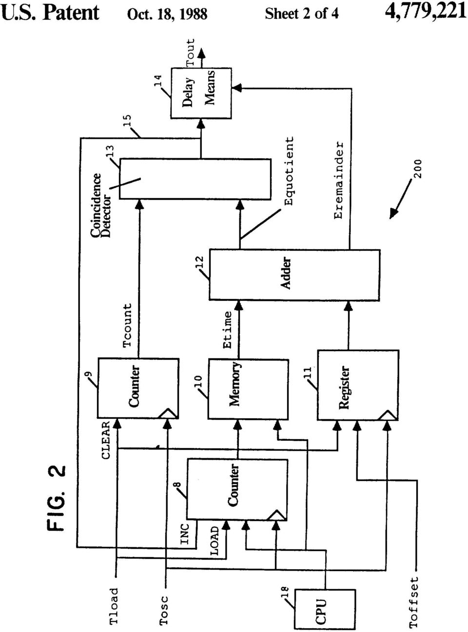
6 1 TIMING SIGNAL GENERATOR 4,779,221 BACKGROUND OF THE INVENTION This invention pertains to timing signal generation, particularly suitable for use in a computerized test sys tem such as that used for testing integrated circuits. Means for testing integrated circuits are well known in the art. Modern systems include the use of a digital computer which is programmed to generate speci?c timing signals for application to a device under test (DUT), and appropriate supply, ground, and other volt ages required to simulate the actual operating environ ment of the DUI. As integrated circuit devices grow larger, the need for more accurate, high speed, inexpen sive, and repeatable testing techniques, including means for generating the appropriate timing signals, are re quired. However, in order to obtain high speed, accu rate, and repeatable timing signals, techniques have been employed which become increasingly expensive. Furthermore, many of these techniques, even though expensive, are not really as accurate or repeatable as desired. One such prior art technique for generating timing signals is described in US. Pat. No. 4,231,104 issued Oct. 28, 1982, St. Clair. St. Clair provides that an oscil lator, such as a crystal oscillator, is used to provide a clock signal. This clock signal is applied to a period generator circuit, which allows a period of desired length to be generated from the crystal oscillator. St. Clair utilizes a counter to count an integral number of clocks from the crystal oscillator and a delay line to interpolate between clock cycles in order that the per iod generated need not have a period equal to an inte gral numberp of clock cycles of the crystal oscillator. Furthermore, St. Clair, due to the manner in which he generates his timing signal edges, requires the period generated to provide two output signals: Tm, which is a delayed version of the crystal oscillator clock signal, 40 and Tom, the actual period signal. St. Clair requires the use of a delay line in order to provide these signals Tgyn and To, so that they are interpolated and thus not nec essarily aligned with the crystal oscillator clock edge. Such delay lines typically comprise a rather long trace 45 on a printed circuit board, thus requiring a rather large area on the printed circuit board and thus being expen sive. Other types of delay lines which can be used are lumped inductor capacitor ladders or networks, which again are expensive. Furthermore, regardless of the type of delay line used, the delay line circuit must be carefully calibrated, thereby requiring additional cali bration circuitry which is expensive and in itself diffi cult to maintain. Furthermore, even once a I5 delay line circuit is calibrated, it is still subject to errors which are dependent on duty cycle and which cannot be removed by further calibration. The delay line circuit can easily drift out of calibration requiring extensive maintenance of the circuit for recalibration, and errors may be in duced due to jitter caused by attenuation of the tim ing signal with an attendant alteration of the rise and fall times, and cross talk between the timing signal passing through the delay line and surrounding signals in the system. Yet another problem with prior art systems is their need to broadcast" variable length Tm signal to many locations in a typical, large system, with inherent degradation in timing occurring due to transmission line effects, and variations among the several transmission 2 lines used for broadcasting to various locations within the system. St. Clair also provides a waveform generator which receives as input signals the Tm and To, signals from the period generator. The waveform generator of St. Clair FIG. 2 includes two edge generator circuits and a wave formatter (60). Each of St. Clair s edge generators includes memory which de?nes the placement of the edge within a period based on coincidence with a counter contained within the waveform generator. Fur thermore, for each edge generator St. Clair provides an additional delay line in order to place the edge at a point which is interpolated between points provided by the period generator. As previously mentioned, these delay line circuits have severe disadvantages. Furthermore, in St. Clair s structure, the delay lines contained within the waveform generator have the potential of delaying the signal up to two times the period of the crystal oscilla tor. This introduces additional error. An additional disadvantage to St. Clair s waveform generator is the fact that each edge generator within the waveform generator can provide only a single edge during a given period. In addition, by the use of the various delay lines in St. Clair, timing signals within the circuit are not synchro nized with the crystal oscillator, thereby making design. calibration, and debugging of such a timing system quite complex and frustrating. SUMMARY In accordance with the teachings of this invention, a unique timing system is provided which allows for a user to program timing events with variable periods and edges from a?xed frequency clock, and having resolu tion greater than that of the?xed reference frequency. In accordance with the teachings of this invention, delay elements, which are inherently expensive, inaccu~ rate, and require repeated calibration, are minimized. BRIEF DESCRIPTION OF THE DRAWINGS FIG. 1 is a block diagram of one embodiment of a period generator constructed in accordance with the teachings of this invention; FIG. 2 is a block diagram of one embodiment of an edge generator constructed in accordance with the teachings of this invention; FIG. 3 is a timing diagram depicting one embodiment of the operation of the strucutures of FIG. 1 and FIG. 2; and FIG. 4 is a block diagram of another embodiment of an edge generator constructed in accordance with the teachings of this invention. DETAILED DESCRIPTION FIG. 1 is a block diagram of one embodiment of a period generator constructed in accordance with the teachings of this invention. Although we refer to the structure of FIG. 1 as a period generator", it will be readily appreciated by those of ordinary skill in the art in light of the teachings of this invention that the period generator of FIG. 1, unlike prior art period generators, does not provide output signals which provide an actual period, but rather provide digital information which de?ne the period. This digital information is used by the edge generator of FIG. 2 (described later) in order to provide the resultant output signals from the edge gen erator of FIG. 2.

7 4,779,221 3 Referring to FIG. 1, oscillator l is any suitable oscil lator, such as a crystal oscillator. For the purpose of this description, certain time periods will be described, al though it is to be understood that the structure of this invention can be implemented using any desired timing periods. For example, oscillator 1 is a crystal oscillator providing a very stable l6 nanosecond period, as is well known in the art. Period generator 100 also includes CPU 18 which serves to load memories 2 and 3 with appropriate information de?ning the period desired to be generated. In order to store appropriate data in mem ories 2 and 3, CPU 18 divides the desired period by the period of oscillator l and determines a C quotient which is the integral number of oscillator 1 clock periods which will?t in the desired period, and the C remain der, which is the interpolation required between clock cycles of oscillator 1. The C quotient is stored in mem ory 2, and the C remainder is stored in memory 3 which are, for example, emitter coupled logic RAMs. In es sence, the actual number stored in memory 2 is a num 20 ber which causes counter 5 to count C quotient clock ticks per period. Counter 5 includes an input lead which receives the oscillator signal from oscillator 1. Counter 5 also in cludes a bus for receiving the number stored in memory 25 2, and a load input lead which causes counter 5 to load the data provided by memory 2 upon receipt of a T1004 signal which is generated when counter 5 has counted C quotient clock signals during this period. Counter 5 provides two output signals, a terminal count signal TC 30 and a terminal count +l signal TC+ l. The TC signal goes active when counter 5 has received C quotient clock signals from oscillator 1, and the TC+1 output signal goes active when counter 5 has received (C quo tient+ l) clock signals from oscillator 1 following the 35 most recent Tlmd signal. It is necessary to provide both output signals TC and TC+ l, with one of the two output signals chosen as a function of C remainder, as described below. Adder 4 serves to provide the summation of C re mainder values required to provide proper interpolation from period to period. For example, for an unchanging period, if C remainder is 2 nanoseconds, during the?rst period the interpolation must be 2 nanoseconds, during the second period, it must be 4 nanoseconds, during the 45 third period it must be 6 nanoseconds, etc. until the interpolation becomes equal to or greater than the per iod of oscillator l, in the example of FIG. 3, l6 nanosec onds. In this event, the T0,, y signal becomes active, causing multiplexer 7 to select the TC + 1 output signal from counter 5 as the Tioad signal. For an embodiment where the period of oscillator l is 16 nanoseconds, and the desired resolution of the period is l nanosecond, adder 4 is a 4-bit adder and C remainder is a 4-bit num ber. This increases by 1 bit for each doubling of the 55 period of oscillator l, or halving of the resolution of the period. Adder 4 provides a carry and a sum output signal to register 6. Register 6 stores the sum received from adder 4 which indicates the interpolation factor required for this period. This interpolation factor is provided on bus 6-1 as data word T-offset. The Tmrry signal is also stored in register 6 and provided on output lead 6-2 to the select input lead of multiplexer 7, which causes multiplexer 7 to select either the TC or TC-l-l signal from counter 5, as required. The To?rmdata is also 65 applied to one input lead of adder 4, causing adder 4 to add the T-offset value with the C remainder value to provide a new carry and sum result for the next period. 4 Thus, period generator 100 provides output signals Tm, the clock signal from oscillator l, and T1004, a signal which restarts the edge generator counter for each period, although not necessarily at the precise beginning of that period, as is more fully described below with regard to the edge generator of FIG. 2. The relationship between the T10 signal and when a new period starts is de?ned by the Tome, data. In accordance with the teachings of this invention, a?xed frequency clock and a digital data word are used to broadcast period and length timing reference information to a plurality of locations, while avoiding the degradation in the clock signal for changing period length, since trans mission line errors for?xed frequency clock signals are easily compensated, as is well known in the art. In one embodiment of this invention, C quotient is the actual quotient as determined by the CPU. In this event, counter 5 counts from 1 to C quotient in response to the output signal from oscillator 1. The TC signal goes active when counter 5 reaches the value of C quotient. and the TC+1 signal goes active when counter 5 reaches C quotient +1. In an alternative embodiment of this invention, memory 2 stores C quotient l, and counter 5, following each load signal, decrements from C quotient 1 to O. In this event, output signal TC goes active when counter 5 reaches 0, and TC + 1 signal goes active when counter 5 reaches l count beyond 0, i.e. rolls over to all ones. This is a particularly attractive approach, since it is quite easy to detect a binary num ber which consists of either all zeros (TC active) or all ones (TC+1 active). FIG. 2 depicts one embodiment of an edge generator constructed in accordance with the teachings of this invention. As will become apparent to those of ordinary skill in the art from the following discussion, edge gen erator 2 is capable of providing a plurality of edges during a signal period, utilizing a single hardware cir cuit and a single delay line. Memory 10 is loaded by CPU 18 prior to testing of a DUT with values calcu lated assuming Toff ; is equal to zero. Edge generator 200 serves to adjust the placement of edges when Tome, is not equal to zero. Memory 10 can include a plurality of data words de?ning a plurality of edges within a period. Also, memory 10 can include a plurality of such sets of data in order to have readily available such a plurality of edge de?nitions for a plurality of different period types. Counter 8 serves to address memory 10 to select the desired data word from memory 10. Counter 8 receives from CPU 18 the base address (i.e. the?rst address within a set of addresses). Alternatively, counter 8 receives this information from a high speed pattern generator, well known in the art. Counter 8 also receives the To signal which allows counter 8, when enabled by active LOAD or INC signals, to change its output state. When the LOAD signal is active, indicat ing a new period, new data from CPU 18 (alternatively a pattern generator, not shown) is loaded into counter 8 in order to access a new page of memory 10. Similarly, when the INC signal is active, counter 8 increments its count to access the next word of the selected page within memory 10, causing memory 10 to provide a data output word de?ning the next edge required to be generated in that period. The data output word from memory 10 can specify that an edge is to be generated within an integral num ber of Tm cycles from the Tload signal, and an interpola tion factor which allows the edge to be generated be tween two adjacent To signals. Furthermore, since

8 4,779,221 5 Tzoad is in fact offset from the period beginning by Toff. m, the Elime data signal from memory 10 and the Tome, value received from period generator 100 of FIG. 1 are added by adder 12 to provide an output signal Ewan-en, and Emmamde, which de?nes precisely where the edge is to be placed with respect to Tom output signal which is enabled by Tload. To affect this, register 11 stores T017, in response to the T1,, signal when clocked by the To,C signal, in order that the Toff, value will be readily available to adder 12. The most signi?cant bits from adder 12 provide the Ewan-em value from adder l2 and the least signi?cant bits provide the Eremm'mje, value from adder 12. In the example where oscillator 1 has a 16 nanosecond period and desired edge placement reso lution is l nanosecond, Equmiem is determined by the longest period desired to be generated and Eremmde, is 4 bits long. Thus, Equotiem de?nes the number of TN signals which must be counted prior to generation of the edge, and Eremainde, de?nes the amount of delay which must be provided by delay line 14 prior to gener 20 ation of the edge. Counter 9 counts Tm signals follow ing its clear by a Tgoad signal. Counter 9 provides a Tmum output signal applied to coincidence detector 13. Coincidence detector 13 provides an output pulse to delay line 14 when T count equals Equo?'em. The amount 25 that this pulse is delayed by delay line 14 is determined by the value of Eremaindw. This provides the desired To, signal which is, for example, applied to a wave formatter (not shown) in order to produce the desired wave form. Such wave formatters are well known in 30 the art and thus will not be described here. The output pulse from coincidence detector 13 is also applied via lead 15 to the INC input lead of counter 8, enabling counter 8 to increment and address the next word of the selected page of memory 10, as previously described. 35 FIG. 3 depicts various timing signals for the embodi ments of FIGS. 1 and 2, when To is 16 nsec, the period length is 52 nsec and T0, pulses are generated at 0 nsec and 24 nsec from a period start. Of importance, a cycle marker is shown in FIG. 3 for reference only, and does not actually appear as an output signal anywhere in the circuit FIG. 4 depicts another embodiment of an edge gener ator 400 constructed in accordance with the teachings of this invention. The structure of FIG. 4 serves to 45 minimize the width of the adder used, thereby simplify ing the circuit and enhancing the speed. The structure of FIG. 4 separates the output bits from memory 10 to provide E?m MSB and Eu'me LSB. The Eame LSB is the interpolation factor stored in memory 10 as loaded by CPU 18. CPU 18 computes Etime LSB and E?me MSB assuming T05, is zero. Edge generator 400 serves to adjust the placement of the edges when Tome; is not equal to zero. En-m LSB and Toff, are added by adder 120 which provides an Eremamder output signal and a 55 carry signal. The Eume MSB is applied to coincidence detector 130 which operates to detect when the number of To clock signals counted by counter 9 is equal to Ema MSB. At this time, coincidence detector 130 pro vides an output signal indicating that an edge is to be generated. The carry signal from adder 120 serves to indicate when the output signal from coincidence detec tor 130 should be delayed a single To count. When required, this single count delay is provided by digital delay circuit 98 which is well known in the art, and in 65 one embodiment comprises a one bit shift register and a multiplexer whih selects either the input signal or the output signal from the one bit shift register. Thus, digi 6 tal and delay circuit 98 delays the output signal from coincidence detector 130 by a single To count, and provides the E remainder signal to delay line 14 follow ing this digital delay. The speci?c embodiments of this invention described in this speci?cation are intended to serve by way of example and are not a limitation on the scope of my invention. Numerous other embodiments of this inven tion will become apparent to those of ordinary skill in the art in light of the teachings of this speci?cation. I claim: 1. A timing system comprising: means for receiving a?xed frequency clock signal; a?rst memory for storing a value which de?nes the number of said clock signals within an output per iod to be generated; a second memory for storing a value which de?nes the fraction of a period of said clock signal needed to be added to said number of said clock signals within an output period in order to provide said output period to be generated; a counter having a first input terminal for receiving said clock signal, a second input terminal for re ceiving a LOAD signal to cause said counter to begin to count clock signals for a new period, a?rst output lead for providing a?rst output signal when said number of said clock signals has been counted, and a second output lead for providing a second output signal when one additional clock signal is counted following said?rst output signal; means for selecting said?rst or said second output signal of said counter as said LOAD signal; an adder for providing a?rst output signal de?ning the fractional portion of a period of said clock signal required to generate said period to be gener ated and adding said value in said second memory and said?rst output signal of the previous adder operation, said adder also providing a second out put signal de?ning when the sum of said value in said second memory and said?rst output signal of the previous adder operation is greater than or equal to the period of said clock signal; means for applying said second output signal of said adder to said means for selecting such that when said second output signal of said adder indicates said sum is greater than or equal to the period of said clock signal said means for selecting selects said second output signal of said counter as said LOAD signal and when said second output signal of said adder indicates said sum is less than the period of said clock signal said means for selecting selects said?rst output signal of said counter as said LOAD signal; wherein said LOAD signal de?nes the start of a new period synchronized to the closest previous clock signal and said?rst output signal of said adder de?nes the relationship between said LOAD signal and the actual start of said period to be generated. 2. The structure of claim 1 wherein said?rst and second memories are loaded from a CPU. 3. The structure of claim 1 wherein said?rst and second memories each contain a plurality of values, each said value de?ning a different period to be gener ated. 4. The structure of claim 1 wherein addressing of said?rst and second memories is controlled by a counter. 5. The structure of claim 3 wherein addressing of said?rst and second memories is controlled by a CPU.

9 7 6. The structure of claim 3 wherein addressing of said?rst and second memories is controlled by a high-speed pattern generator. 7. The structure as in claim 1 wherein said?rst output signal of said adder is a sum and said second output signal of said adder is a carry 4,779, The structure as in claim 1 wherein said means for applying is a register. 9. The structure as in claim 7 wherein said register is enabled to load by said LOAD signal. 10. The structure as in claim 8 wherein said LOAD signal is synchronous with said clock signal. 11. The structure as in claim 1 wherein operation is synchronous with said clock signal. # 1 i I i

(12) (10) Patent N0.: US 6,614,314 B2 d Haene et al. 45 Date 0f Patent: Se. 2 2003 (54) NON-LINEAR PHASE DETECTOR FOREIGN PATENT DOCUMENTS
 (10) Patent N0.: US 6,614,314 B2 d Haene et al. 45 Date 0f Patent: Se. 2 2003 (54) NON-LINEAR PHASE DETECTOR FOREIGN PATENT DOCUMENTS") United States Patent US006614314B2 (12) (10) Patent N0.: US 6,614,314 B2 d Haene et al. 45 Date 0f Patent: Se. 2 2003 a (54) NON-LINEAR PHASE DETECTOR FOREIGN PATENT DOCUMENTS (75) Inventors: Wesley Calvin
United States Patent US006614314B2 (12) (10) Patent N0.: US 6,614,314 B2 d Haene et al. 45 Date 0f Patent: Se. 2 2003 a (54) NON-LINEAR PHASE DETECTOR FOREIGN PATENT DOCUMENTS (75) Inventors: Wesley Calvin
Hay (43) Pub. Date: Oct. 17, 2002
 Pub. Date: Oct. 17, 2002") US 20020152322A1 (19) United States (12) Patent Application Publication (10) Pub. No.: US 2002/0152322 A1 Hay (43) Pub. Date: Oct. 17, 2002 (54) (76) (21) (22) (51) (52) METHOD AND APPARATUS FOR FACILITATING
US 20020152322A1 (19) United States (12) Patent Application Publication (10) Pub. No.: US 2002/0152322 A1 Hay (43) Pub. Date: Oct. 17, 2002 (54) (76) (21) (22) (51) (52) METHOD AND APPARATUS FOR FACILITATING
US 20090157756Al (19) United States (12) Patent Application Publication (10) Pub. No.: US 2009/0157756 A1 Sanvido (43) Pub. Date: Jun.
 United States (12) Patent Application Publication (10) Pub. No.: US 2009/0157756 A1 Sanvido (43) Pub. Date: Jun.") US 20090157756Al (19) United States (12) Patent Application Publication (10) Pub. No.: US 2009/0157756 A1 Sanvido (43) Pub. Date: Jun. 18, 2009 (54) FILE SYSTEM FOR STORING FILES IN Publication Classi?cation
US 20090157756Al (19) United States (12) Patent Application Publication (10) Pub. No.: US 2009/0157756 A1 Sanvido (43) Pub. Date: Jun. 18, 2009 (54) FILE SYSTEM FOR STORING FILES IN Publication Classi?cation
\ \ \ connection connection connection interface interface interface
 US 20140122910A1 (19) United States (12) Patent Application Publication (10) Pub. No.: US 20140122910 A1 Chiu et al. (43) Pub. Date: May 1, 2014 (54) RACK SERVER SYSTEM AND OPERATION Publication Classi?cation
71M6521 Energy Meter IC. Real Time Clock Compensation. The Challenge. The RTC in the 71M6521D/F. Theory of Operation APPLICATION NOTE
 71M6521 Energy Meter IC A Maxim Integrated Products Brand APPLICATION NOTE AN_6521_035 MAY 2007 This document describes how to use software to compensate the real time clock (RTC) in Teridian meter chips.
US 20140046812A1 (19) United States (12) Patent Application Publication (10) Pub. No.: US 2014/0046812 A1 FAN et al. (43) Pub. Date: Feb.
 United States (12) Patent Application Publication (10) Pub. No.: US 2014/0046812 A1 FAN et al. (43) Pub. Date: Feb.") US 20140046812A1 (19) United States (12) Patent Application Publication (10) Pub. No.: US 2014/0046812 A1 FAN et al. (43) Pub. Date: (54) EXPENSE REPORTS FOR PAYMENTS MADE (52) US. Cl. WITH A MOBILE DEVICE
US 20140046812A1 (19) United States (12) Patent Application Publication (10) Pub. No.: US 2014/0046812 A1 FAN et al. (43) Pub. Date: (54) EXPENSE REPORTS FOR PAYMENTS MADE (52) US. Cl. WITH A MOBILE DEVICE
United States Patent [191
 United States Patent [191 Fancy [54] REDUNDANT SIGNAL CIRCUIT [75] Inventor: Thomas A. Fancy, Westminster, Mass. [73] Assignee: General Electric Company, Schenectady, NY. [211 Appl. No.: 854,973 [22] Filed:
USOO5408501A United States Patent [191 [11] Patent Number: 5,408,501 Cornaby [45] Date of Patent: Apr. 18, 1995
![USOO5408501A United States Patent [191 [11] Patent Number: 5,408,501 Cornaby [45] Date of Patent: Apr. 18, 1995](/thumbs/25/5421507.jpg "USOO5408501A United States Patent [191 [11] Patent Number: 5,408,501 Cornaby [45] Date of Patent: Apr. 18, 1995") USOO5408501A United States Patent [191 [11] Patent Number: 5,408,501 Cornaby [45] Date of Patent: Apr. 18, 1995 [54] DATA TRANSFER SYSTEM [57] ABSTRACT [75] Inventor: Stephen R. Cornaby, Niwot, Colo. A
USOO5408501A United States Patent [191 [11] Patent Number: 5,408,501 Cornaby [45] Date of Patent: Apr. 18, 1995 [54] DATA TRANSFER SYSTEM [57] ABSTRACT [75] Inventor: Stephen R. Cornaby, Niwot, Colo. A
US 20020072350A1 (19) United States (12) Patent Application Publication (10) Pub. No.: US 2002/0072350 A1 Fukuzato (43) Pub. Date: Jun.
 United States (12) Patent Application Publication (10) Pub. No.: US 2002/0072350 A1 Fukuzato (43) Pub. Date: Jun.") US 20020072350A1 (19) United States (12) Patent Application Publication (10) Pub. No.: US 20020072350 A1 Fukuzato (43) Pub. Date: Jun. 13, 2002 (54) BACKUP METHOD OF APPLICATIONS OF PORTABLE CELLULAR PHONE
US 20020072350A1 (19) United States (12) Patent Application Publication (10) Pub. No.: US 20020072350 A1 Fukuzato (43) Pub. Date: Jun. 13, 2002 (54) BACKUP METHOD OF APPLICATIONS OF PORTABLE CELLULAR PHONE
MAIN COMPUTER MONlTOR. INPUT/ OUTPUT ClRCUlT. 4,748,566 May 31, 1988. United States Patent [191. [11] Patent Number: [45] Date of Patent:
![MAIN COMPUTER MONlTOR. INPUT/ OUTPUT ClRCUlT. 4,748,566 May 31, 1988. United States Patent [191. [11] Patent Number: [45] Date of Patent:](/thumbs/29/13384343.jpg "MAIN COMPUTER MONlTOR. INPUT/ OUTPUT ClRCUlT. 4,748,566 May 31, 1988. United States Patent [191. [11] Patent Number: [45] Date of Patent:") United States Patent [191 Sasaki et al. [11] Patent Number: [45] Date of Patent: May 31, 1988 [54] ENGINE CONTROL APPARATUS [75] Inventors: Shoji Sasaki; Kenji Tabuchi, both of Katsuta, Japan [73] Assignee:
United States Patent [191 Sasaki et al. [11] Patent Number: [45] Date of Patent: May 31, 1988 [54] ENGINE CONTROL APPARATUS [75] Inventors: Shoji Sasaki; Kenji Tabuchi, both of Katsuta, Japan [73] Assignee:
(12) United States Patent (10) Patent N0.: US 7,068,424 B1 Jennings et al. (45) Date of Patent: Jun. 27, 2006
 United States Patent (10) Patent N0.: US 7,068,424 B1 Jennings et al. (45) Date of Patent: Jun. 27, 2006") US007068424B1 (12) United States Patent (10) Patent N0.: US 7,068,424 B1 Jennings et al. (45) Date of Patent: Jun. 27, 2006 (54) MULTIPLE PULSE GENERATION 6,141,127 A * 10/2000 Boivin et a1...... 398/92
US007068424B1 (12) United States Patent (10) Patent N0.: US 7,068,424 B1 Jennings et al. (45) Date of Patent: Jun. 27, 2006 (54) MULTIPLE PULSE GENERATION 6,141,127 A * 10/2000 Boivin et a1...... 398/92
(54) RETARGETING RELATED TECHNIQUES (52) US. Cl... 705/1453 AND OFFERINGS. (75) Inventors: Ayrnan Farahat, San Francisco, (57) ABSTRACT
 RETARGETING RELATED TECHNIQUES (52) US. Cl... 705/1453 AND OFFERINGS. (75) Inventors: Ayrnan Farahat, San Francisco, (57) ABSTRACT") US 20120271714Al (19) United States (12) Patent Application Publication (10) Pub. N0.: US 2012/0271714 A1 Farahat et a]. (43) Pub. Date: Oct. 25, 2012 (54) RETARGETING RELATED TECHNIQUES (52) US. Cl......
US 20120271714Al (19) United States (12) Patent Application Publication (10) Pub. N0.: US 2012/0271714 A1 Farahat et a]. (43) Pub. Date: Oct. 25, 2012 (54) RETARGETING RELATED TECHNIQUES (52) US. Cl......
(12) United States Patent Halonen
 United States Patent Halonen") (12) United States Patent Halonen US006334053B1 () Patent N0.: (45) Date of Patent: Dec. 25, 2001 (54) PROCEDURE AND SYSTEM FOR PROVIDING AN ANSWERING SERVICE (75) Inventor: Mikko Halonen, Oulu (Fl) (73)
(12) United States Patent Halonen US006334053B1 () Patent N0.: (45) Date of Patent: Dec. 25, 2001 (54) PROCEDURE AND SYSTEM FOR PROVIDING AN ANSWERING SERVICE (75) Inventor: Mikko Halonen, Oulu (Fl) (73)
United States Patent [191 [11] 4,388,717 Burke [45] Jun. 14, 1983
![United States Patent [191 [11] 4,388,717 Burke [45] Jun. 14, 1983](/thumbs/26/7153231.jpg "United States Patent [191 [11] 4,388,717 Burke [45] Jun. 14, 1983") ,. United States Patent [191 [11] 4,3,717 Burke [45] Jun. 14, 193 [54] CONFERENCE CIRCUIT FOR PCM SYSTEM Primary Examiner-Jin F. Ng [75] Inventor: Michael G. Burke, Corinth, Miss. 33g? gent or Firm James
,. United States Patent [191 [11] 4,3,717 Burke [45] Jun. 14, 193 [54] CONFERENCE CIRCUIT FOR PCM SYSTEM Primary Examiner-Jin F. Ng [75] Inventor: Michael G. Burke, Corinth, Miss. 33g? gent or Firm James
llllllllllllllillllllllllllllllllllllllllllllllllllllllllllllllllllllllllll
 llllllllllllllillllllllllllllllllllllllllllllllllllllllllllllllllllllllllll USOO5535162A United States Patent [19] [11] Patent Number: 5,535,162 Uenoyama [45] Date of Patent: Jul. 9, 1996 [54] ELECTRICALLY
Telephone Dressing Systems - Advantages and Disadvantages
 I US 20030185352A1 (19) United States (12) Patent Application Publication (10) Pub. No.: US 2003/0185352 A1 Savage et al. (43) Pub. Date: (54) AUTOMATED MESSAGE BROADCAST SYSTEM WITH DUAL MESSAGE SOURCES
(54) RAPID NOTIFICATION SYSTEM (52) US. Cl... 709/206. (57) ABSTRACT (75) Inventors: Anand Rajasekar, San Jose, CA
 RAPID NOTIFICATION SYSTEM (52) US. Cl... 709/206. (57) ABSTRACT (75) Inventors: Anand Rajasekar, San Jose, CA") US 20120303720A1 (19) United States (12) Patent Application Publication (10) Pub. N0.: US 2012/0303720 A1 Rajasekar et a]. (43) Pub. Date: NOV. 29, 2012 (54) RAPID NOTIFICATION SYSTEM (52) US. Cl......
US 20120303720A1 (19) United States (12) Patent Application Publication (10) Pub. N0.: US 2012/0303720 A1 Rajasekar et a]. (43) Pub. Date: NOV. 29, 2012 (54) RAPID NOTIFICATION SYSTEM (52) US. Cl......
(Us) (73) Assignee: Avaya Technology Corp. Je?' McElroy, Columbia, SC (US); (21) Appl. No.: 10/413,024. (22) Filed: Apr. 14, 2003 (57) ABSTRACT
 (73) Assignee: Avaya Technology Corp. Je?' McElroy, Columbia, SC (US); (21) Appl. No.: 10/413,024. (22) Filed: Apr. 14, 2003 (57) ABSTRACT") US 20040202300A1 (19) United States (12) Patent Application Publication (10) Pub. No.: US 2004/0202300 A1 Cooper et al. (43) Pub. Date: Oct. 14, 2004 (54) CALL HANDLING USING NON-SPEECH CUES VIA A PERSONAL
US 20040202300A1 (19) United States (12) Patent Application Publication (10) Pub. No.: US 2004/0202300 A1 Cooper et al. (43) Pub. Date: Oct. 14, 2004 (54) CALL HANDLING USING NON-SPEECH CUES VIA A PERSONAL
Means are provided for repetitively applying a low [52] U S Cl 128/2 1 B 324/51 current signal, having a distinctive waveform and fre
![Means are provided for repetitively applying a low [52] U S Cl 128/2 1 B 324/51 current signal, having a distinctive waveform and fre](/thumbs/34/17190383.jpg "Means are provided for repetitively applying a low [52] U S Cl 128/2 1 B 324/51 current signal, having a distinctive waveform and fre") United States Patent [19] [111 Lencioni, Jr. [451 Jan. 14, 1975 [54] OPEN LEAD TESTING SYSTEM FOR EEG Primary Examiner William E. Kamm [75] Inventor: Cecil C. Lencioni, Jr., Chicago, Ill. giggles; Agent
United States Patent [19] [111 Lencioni, Jr. [451 Jan. 14, 1975 [54] OPEN LEAD TESTING SYSTEM FOR EEG Primary Examiner William E. Kamm [75] Inventor: Cecil C. Lencioni, Jr., Chicago, Ill. giggles; Agent
POTENTIAL. SC DA Il'JA N INTERFACE m. (21) Appl. No.: 11/037,604
 Appl. No.: 11/037,604") US 20050125439A1 (19) United States (12) Patent Application Publication (10) Pub. No.: US 2005/0125439 A1 Nourbakhsh et al. (43) Pub. Date: Jun. 9, 2005 (54) METHOD AND APPARATUS FOR MULTI-CONTACT SCHEDULING
US 20050125439A1 (19) United States (12) Patent Application Publication (10) Pub. No.: US 2005/0125439 A1 Nourbakhsh et al. (43) Pub. Date: Jun. 9, 2005 (54) METHOD AND APPARATUS FOR MULTI-CONTACT SCHEDULING
wanagamem transformation and management
 US 20120150919Al (19) United States (12) Patent Application Publication (10) Pub. No.: US 2012/0150919 A1 Brown et al. (43) Pub. Date: Jun. 14, 2012 (54) (76) (21) (22) (60) (51) AGENCY MANAGEMENT SYSTEM
US 20070016324A1 (19) United States (12) Patent Application Publication (10) Pub. No.: US 2007/0016324 A1. Operating System. 106 q f 108.
 United States (12) Patent Application Publication (10) Pub. No.: US 2007/0016324 A1. Operating System. 106 q f 108.") US 20070016324A1 (19) United States (12) Patent Application Publication (10) Pub. No.: US 2007/0016324 A1 Oddiraj u et al. (43) Pub. Date: Jan. 18, 2007 (54) SYSTEM BOOT OPTMZER (75) nventors: Chandar
US 20070016324A1 (19) United States (12) Patent Application Publication (10) Pub. No.: US 2007/0016324 A1 Oddiraj u et al. (43) Pub. Date: Jan. 18, 2007 (54) SYSTEM BOOT OPTMZER (75) nventors: Chandar
Hearing Aids And Frequency Response Testing
 ' United States Patent [191 1 Power et al. [54] FREQUENCY RESPONSE TESTING APPARATUS [75] Inventors: Ronald Frederick Power, Rayleigh; Alan Anthony Barker, Gravesend; Michael Charles Martin, Kingston-upon-Thames;
US 20020174380A1 (19) United States (12) Patent Application Publication (10) Pub. N0.: US 2002/0174380 A1. Mannarsamy (43) Pub. Date: NOV.
 United States (12) Patent Application Publication (10) Pub. N0.: US 2002/0174380 A1. Mannarsamy (43) Pub. Date: NOV.") US 20020174380A1 (19) United States (12) Patent Application Publication (10) Pub. N0.: US 2002/0174380 A1 Mannarsamy (43) Pub. Date: NOV. 21, 2002 (54) HELPDESK SYSTEM AND METHOD (52) US. Cl...... 714/25
US 20020174380A1 (19) United States (12) Patent Application Publication (10) Pub. N0.: US 2002/0174380 A1 Mannarsamy (43) Pub. Date: NOV. 21, 2002 (54) HELPDESK SYSTEM AND METHOD (52) US. Cl...... 714/25
US 20020116467A1 (19) United States (12) Patent Application Publication (10) Pub. No.: US 2002/0116467 A1 Boyer et al. (43) Pub. Date: Aug.
 United States (12) Patent Application Publication (10) Pub. No.: US 2002/0116467 A1 Boyer et al. (43) Pub. Date: Aug.") US 20020116467A1 (19) United States (12) Patent Application Publication (10) Pub. No.: US 2002/0116467 A1 Boyer et al. (43) Pub. Date: Aug. 22, 2002 (54) METHOD AND APPARATUS FOR Publication Classi?cation
US 20020116467A1 (19) United States (12) Patent Application Publication (10) Pub. No.: US 2002/0116467 A1 Boyer et al. (43) Pub. Date: Aug. 22, 2002 (54) METHOD AND APPARATUS FOR Publication Classi?cation
United States Patent [191 Brugliera et al.
 United States Patent [191 Brugliera et al. [11] [45] Patent Number: 4,910,767 Date of Patent: Mar. 20, 1990 [54] [75] [73] [21] [22] [51] [52] [58] [56] ANI AUTO DIALER WITH CARRIER CURRENT INTERFACE Inventors:
Ulllted States Patent [19] [11] Patent Number: 5,943,406
![Ulllted States Patent [19] [11] Patent Number: 5,943,406](/thumbs/30/14188909.jpg "Ulllted States Patent [19] [11] Patent Number: 5,943,406") US005943406A Ulllted States Patent [19] [11] Patent Number: 5,943,406 Leta et al. [45] Date of Patent: Aug. 24, 1999 [54] TELEPHONE CALL TRACKING AND 4,813,065 3/1989 Segala..... 379/112 BILLING SYSTEM
US005943406A Ulllted States Patent [19] [11] Patent Number: 5,943,406 Leta et al. [45] Date of Patent: Aug. 24, 1999 [54] TELEPHONE CALL TRACKING AND 4,813,065 3/1989 Segala..... 379/112 BILLING SYSTEM
AN_6521_035 APRIL 2009
 71M6521 Energy Meter IC A Maxim Integrated Products Brand APPLICATION NOTE AN_6521_035 APRIL 2009 This document describes how to use software to compensate the real time clock (RTC) in Teridian meter chips.
Asynchronous counters, except for the first block, work independently from a system clock.
 Counters Some digital circuits are designed for the purpose of counting and this is when counters become useful. Counters are made with flip-flops, they can be asynchronous or synchronous and they can
Naylor, Lake OsWego, OR (US) (51) Int_ CL
 (51) Int_ CL") US 20100023688A1 (19) United States (12) Patent Application Publication (10) Pub. No.: US 2010/0023688 A1 Crowther et al. (43) Pub. Date: (54) SYMMETRICAL STORAGE ACCESS ON (86) PCT No.: PCT/US2007/001542
US 20100023688A1 (19) United States (12) Patent Application Publication (10) Pub. No.: US 2010/0023688 A1 Crowther et al. (43) Pub. Date: (54) SYMMETRICAL STORAGE ACCESS ON (86) PCT No.: PCT/US2007/001542
US 20130007621A1 (19) United States (12) Patent Application Publication (10) Pub. No.: US 2013/0007621 A1 Warren (43) Pub. Date: Jan.
 United States (12) Patent Application Publication (10) Pub. No.: US 2013/0007621 A1 Warren (43) Pub. Date: Jan.") US 20130007621A1 (19) United States (12) Patent Application Publication (10) Pub. No.: US 2013/0007621 A1 Warren (43) Pub. Date: Jan. 3, 2013 (54) (76) (21) (22) (51) (52) SYSTEM FOR LEARNING NAMES OF
US 20130007621A1 (19) United States (12) Patent Application Publication (10) Pub. No.: US 2013/0007621 A1 Warren (43) Pub. Date: Jan. 3, 2013 (54) (76) (21) (22) (51) (52) SYSTEM FOR LEARNING NAMES OF
US 20130169877A1 (19) United States (12) Patent Application Publication (10) Pub. N0.: US 2013/0169877 A1 DANG (43) Pub. Date: Jul.
 United States (12) Patent Application Publication (10) Pub. N0.: US 2013/0169877 A1 DANG (43) Pub. Date: Jul.") US 20130169877A1 (19) United States (12) Patent Application Publication (10) Pub. N0.: US 2013/0169877 A1 DANG (43) Pub. Date: Jul. 4, 2013 (54) SUPPLEMENTAL AUDIO AND VISUAL (52) US. Cl. SYSTEM FORA VIDEO
US 20130169877A1 (19) United States (12) Patent Application Publication (10) Pub. N0.: US 2013/0169877 A1 DANG (43) Pub. Date: Jul. 4, 2013 (54) SUPPLEMENTAL AUDIO AND VISUAL (52) US. Cl. SYSTEM FORA VIDEO
US 20070139188A1 (19) United States (12) Patent Application Publication (10) Pub. No.: US 2007/0139188 A1 Ollis et al. HOME PROCESSOR /\ J\ NETWORK
 United States (12) Patent Application Publication (10) Pub. No.: US 2007/0139188 A1 Ollis et al. HOME PROCESSOR /\ J\ NETWORK") US 20070139188A1 (19) United States (12) Patent Application Publication (10) Pub. No.: US 2007/0139188 A1 Ollis et al. (43) Pub. Date: Jun. 21, 2007 (54) (75) (73) (21) (22) METHOD AND APPARATUS FOR COMMUNICATING
US 20070139188A1 (19) United States (12) Patent Application Publication (10) Pub. No.: US 2007/0139188 A1 Ollis et al. (43) Pub. Date: Jun. 21, 2007 (54) (75) (73) (21) (22) METHOD AND APPARATUS FOR COMMUNICATING
Timing Errors and Jitter
 Timing Errors and Jitter Background Mike Story In a sampled (digital) system, samples have to be accurate in level and time. The digital system uses the two bits of information the signal was this big
(12) Patent Application Publication (10) Pub. No.: US 2003/0035525 A1 Wu et al. (43) Pub. Date: Feb. 20, 2003
 Patent Application Publication (10) Pub. No.: US 2003/0035525 A1 Wu et al. (43) Pub. Date: Feb. 20, 2003") (19) United States US 20030035525A1 (12) Patent Application Publication (10) Pub. No.: US 2003/0035525 A1 Wu et al. (43) Pub. Date: (54) (76) (21) (22) SYSTEM AND METHOD FOR DISTINGUISHING TELEPHONE NUMBER
(19) United States US 20030035525A1 (12) Patent Application Publication (10) Pub. No.: US 2003/0035525 A1 Wu et al. (43) Pub. Date: (54) (76) (21) (22) SYSTEM AND METHOD FOR DISTINGUISHING TELEPHONE NUMBER
. tlllll,1! 1% 11:11 I.,W/ "-111 // out AIHI/ ) I \\ M10. 1 I! (1' 1L- 1!!! I VEHICLE} I] r20 (TRAFFIC COMPUTER 10 RECEIVING UNIT 41 I \ ")SENSOR
![. tlllll,1! 1% 11:11 I.,W/ -111 // out AIHI/ ) I \\ M10. 1 I! (1' 1L- 1!!! I VEHICLE} I] r20 (TRAFFIC COMPUTER 10 RECEIVING UNIT 41 I \ )SENSOR](/thumbs/32/15591097.jpg ". tlllll,1! 1% 11:11 I.,W/ -111 // out AIHI/ ) I \\ M10. 1 I! (1' 1L- 1!!! I VEHICLE} I] r20 (TRAFFIC COMPUTER 10 RECEIVING UNIT 41 I \ )SENSOR") United States Patent [19] Albrecht et al. US005812069A [11] Patent Number: [] Date of Patent: Sep. 22, 1998 [54] METHOD AND SYSTEM FOR FORECASTING TRAFFIC FLOWS [75] Inventors: UWe Albrecht, Miinchen;
United States Patent [19] Albrecht et al. US005812069A [11] Patent Number: [] Date of Patent: Sep. 22, 1998 [54] METHOD AND SYSTEM FOR FORECASTING TRAFFIC FLOWS [75] Inventors: UWe Albrecht, Miinchen;
How To Make A Programmable Logic Network From A Program To A Program
 Àug.19,19694 c. CHEMLA :TAL ' 3,462,738. _ POLYPHASE PRIORITY DETERMINING SYSTEM Filed May 19, 1966 s sheets-*sheet x l I I I ` ` i i tu t1 t2 t3 t1. t5 te t7 te ts îlo tu t1: ha tu. BY mventors. clauos
4,670,900 Jun. 2, 1987
 United States Patent [19] Waldman [11] Patent Number: [45] Date of Patent: 4,670,900 Jun. 2, 1987 [54] SINGLE LINE TELEPHONE CALL FORWARDING DEVICE [76] Inventor: Herbert H. Waldman, 1739 52nd St., Brooklyn,
High Availability Server Supports Dependable Infrastructures
 High Availability Server Supports Dependable Infrastructures MIZUTANI Fumitoshi, ABE Shinji Abstract Since IT devices permeate the social infrastructure as life lines that support the ubiquitous society,
(71) Applicant: SPEAKWRITE, LLC,Austin, TX (US)
 Applicant: SPEAKWRITE, LLC,Austin, TX (US)") US 20130304465Al (19) United States (12) Patent Application Publication (10) Pub. No.: US 2013/0304465 A1 Henry et al. (43) Pub. Date: NOV. 14, 2013 (54) METHOD AND SYSTEM FOR AUDIO-VIDEO (52) US. Cl.
US 20130304465Al (19) United States (12) Patent Application Publication (10) Pub. No.: US 2013/0304465 A1 Henry et al. (43) Pub. Date: NOV. 14, 2013 (54) METHOD AND SYSTEM FOR AUDIO-VIDEO (52) US. Cl.
US 20130138449A1 (19) United States (12) Patent Application Publication (10) Pub. N0.: US 2013/0138449 A1 Pi0t (43) Pub. Date: May 30, 2013
 United States (12) Patent Application Publication (10) Pub. N0.: US 2013/0138449 A1 Pi0t (43) Pub. Date: May 30, 2013") US 20130138449A1 (19) United States (12) Patent Application Publication (10) Pub. N0.: US 2013/0138449 A1 Pi0t (43) Pub. Date: May 30, 2013 (54) SYSTEM AND METHOD FOR SCHEDULING (52) us. c1. HoME VISITS
US 20130138449A1 (19) United States (12) Patent Application Publication (10) Pub. N0.: US 2013/0138449 A1 Pi0t (43) Pub. Date: May 30, 2013 (54) SYSTEM AND METHOD FOR SCHEDULING (52) us. c1. HoME VISITS
Decimal Number (base 10) Binary Number (base 2)
 Binary Number (base 2)") LECTURE 5. BINARY COUNTER Before starting with counters there is some vital information that needs to be understood. The most important is the fact that since the outputs of a digital chip can only be
LECTURE 5. BINARY COUNTER Before starting with counters there is some vital information that needs to be understood. The most important is the fact that since the outputs of a digital chip can only be
60 REDIRECTING THE PRINT PATH MANAGER 1
 US006788429B1 (12) United States Patent (10) Patent No.: US 6,788,429 B1 Clough et al. (45) Date of Patent: Sep. 7, 2004 (54) REMOTE PRINT QUEUE MANAGEMENT FOREIGN PATENT DOCUMENTS (75) Inventors: James
: 2R5 ML OR 2. United States Patent [191. Fig-A3 [111 3,909,553. [451 Sept. 30, 1975 C54 ( T : Marshall. Laboratories Incorporated, Northlake, Ill.
 United States Patent [191 Marshall [111 3,909,553 [451 Sept. 30, 1975 I54] LINE CARD FOR KEY TELEPHONE SYSTEMS ADAPTED TO PROVIDE MUSIC DURING HOLD CONDITION [75] Inventor: Richard A. Marshall, Bensenville.
Wiki Lab Book. This week is practice for wiki usage during the project.
 Wiki Lab Book Use a wiki as a lab book. Wikis are excellent tools for collaborative work (i.e. where you need to efficiently share lots of information and files with multiple people). This week is practice
222252 211222 1111;111:131... ~~~~~~~~~~~~~~~~~~~ 2221522 [73] Assigneez Rockwell Semiconductor Systems 5,754,639 5/1998 Flockhart et al...
![222252 211222 1111;111:131... ~~~~~~~~~~~~~~~~~~~ 2221522 [73] Assigneez Rockwell Semiconductor Systems 5,754,639 5/1998 Flockhart et al...](/thumbs/31/14952948.jpg "222252 211222 1111;111:131... ~~~~~~~~~~~~~~~~~~~ 2221522 [73] Assigneez Rockwell Semiconductor Systems 5,754,639 5/1998 Flockhart et al...") I I US0059012A Ulllted States Patent [19] [11] Patent Number: Dez0nn0 [] Date of Patent: * May 4, 1999 [54] APPARATUS AND METHOD FOR 5,526,416 6/1996 DeZonno et al...... 379/266 IDENTIFYING RECORDS ()1?
I I US0059012A Ulllted States Patent [19] [11] Patent Number: Dez0nn0 [] Date of Patent: * May 4, 1999 [54] APPARATUS AND METHOD FOR 5,526,416 6/1996 DeZonno et al...... 379/266 IDENTIFYING RECORDS ()1?
(12) (10) Patent N0.: US 7,069,466 B2 Trimmer et a]. (45) Date of Patent: Jun. 27, 2006
![(12) (10) Patent N0.: US 7,069,466 B2 Trimmer et a]. (45) Date of Patent: Jun. 27, 2006](/thumbs/33/15766535.jpg "(12) (10) Patent N0.: US 7,069,466 B2 Trimmer et a]. (45) Date of Patent: Jun. 27, 2006") United States Patent US007069466B2 (12) (10) Patent N0.: US 7,069,466 B2 Trimmer et a]. (45) Date of Patent: Jun. 27, 2006 (54) METHOD AND SYSTEM FOR COPYING 5,963,971 A 10/1999 Fosler et a1. BACKUP DATA
United States Patent US007069466B2 (12) (10) Patent N0.: US 7,069,466 B2 Trimmer et a]. (45) Date of Patent: Jun. 27, 2006 (54) METHOD AND SYSTEM FOR COPYING 5,963,971 A 10/1999 Fosler et a1. BACKUP DATA
US 20120215907A1 (19) United States (12) Patent Application Publication (10) Pub. No.: US 2012/0215907 A1 Chung (43) Pub. Date: Aug.
 United States (12) Patent Application Publication (10) Pub. No.: US 2012/0215907 A1 Chung (43) Pub. Date: Aug.") US 20120215907A1 (19) United States (12) Patent Application Publication (10) Pub. No.: US 2012/0215907 A1 Chung (43) Pub. Date: (54) SYSTEMS AND METHODS FOR (52) US. Cl...... 709/224 SELF-ADJUSTING LOGGING
US 20120215907A1 (19) United States (12) Patent Application Publication (10) Pub. No.: US 2012/0215907 A1 Chung (43) Pub. Date: (54) SYSTEMS AND METHODS FOR (52) US. Cl...... 709/224 SELF-ADJUSTING LOGGING
US 20060209260A1 (19) United States (12) Patent Application Publication (10) Pub. No.: US 2006/0209260 A1 Clegg (43) Pub. Date: Sep.
 United States (12) Patent Application Publication (10) Pub. No.: US 2006/0209260 A1 Clegg (43) Pub. Date: Sep.") US 20060209260A1 (19) United States (12) Patent Application Publication (10) Pub. No.: Clegg (43) Pub. Date: Sep. 21, 2006 (54) SCROLLING PICTURE CHANGER (52) US. Cl...... 352/98 (76) Inventor: Timothy
US 20060209260A1 (19) United States (12) Patent Application Publication (10) Pub. No.: Clegg (43) Pub. Date: Sep. 21, 2006 (54) SCROLLING PICTURE CHANGER (52) US. Cl...... 352/98 (76) Inventor: Timothy
Cunneciiun to credit cards dltabase. The system analyzes all credit cards aeecums.
 US 20050137949A1 (19) United States (12) Patent Application Publication (10) Pub. No.: US 2005/0137949 A1 Rittman et al. (43) Pub. Date: Jun. 23, 2005 (54) AUTOMATIC, CHARACTERIZED AND PRIORITIZED TRANSACTIONS
(12) United States Patent (16) Patent N6.= US 6,198,814 B1 Gill (45) Date of Patent: Mar. 6, 2001
 United States Patent (16) Patent N6.= US 6,198,814 B1 Gill (45) Date of Patent: Mar. 6, 2001") US006198814B1 (12) United States Patent (16) Patent N6.= Gill (45) Date of Patent: Mar. 6, 2001 (54) SYSTEM AND METHOD FOR ENTERING 5,621,790 * 4/1997 Grossman 6161...... 379/266 CALL OUTCOME RECORDS IN
US006198814B1 (12) United States Patent (16) Patent N6.= Gill (45) Date of Patent: Mar. 6, 2001 (54) SYSTEM AND METHOD FOR ENTERING 5,621,790 * 4/1997 Grossman 6161...... 379/266 CALL OUTCOME RECORDS IN
A PC-BASED TIME INTERVAL COUNTER WITH 200 PS RESOLUTION
 35'th Annual Precise Time and Time Interval (PTTI) Systems and Applications Meeting San Diego, December 2-4, 2003 A PC-BASED TIME INTERVAL COUNTER WITH 200 PS RESOLUTION Józef Kalisz and Ryszard Szplet
(12) United States Patent (10) Patent No.: US 8,253,226 B2 Oguri (45) Date of Patent: Aug. 28, 2012
 United States Patent (10) Patent No.: US 8,253,226 B2 Oguri (45) Date of Patent: Aug. 28, 2012") US008253226B2 (12) United States Patent (10) Patent No.: US 8,253,226 B2 Oguri (45) Date of Patent: Aug. 28, 2012 (54) ELECTRONIC PARTS, AND METHOD FOR (56) References Cited ARRANGING SHIELDING CASE AND
US008253226B2 (12) United States Patent (10) Patent No.: US 8,253,226 B2 Oguri (45) Date of Patent: Aug. 28, 2012 (54) ELECTRONIC PARTS, AND METHOD FOR (56) References Cited ARRANGING SHIELDING CASE AND
The enable pin needs to be high for data to be fed to the outputs Q and Q bar.
 of 7 -Type flip-flop (Toggle switch) The -type flip-flops are used in prescalar/divider circuits and frequency phase detectors. Figure shows how the flip-flop (latch) can be made using -input logic circuits
(43) Pub. Date: Feb. 16, 2012
 Pub. Date: Feb. 16, 2012") US 20120041897A1 (19) United States (12) Patent Application Publication (10) Pub. No.: US 2012/0041897 A1 Teague et al. (43) Pub. Date: (54) (75) (73) (21) (22) (63) MARKET INDICATOR PROCESS AND METHOD
US 20120041897A1 (19) United States (12) Patent Application Publication (10) Pub. No.: US 2012/0041897 A1 Teague et al. (43) Pub. Date: (54) (75) (73) (21) (22) (63) MARKET INDICATOR PROCESS AND METHOD
check is encoded for causing it to b; oplerable with a, predetermined metering device. In t e a ternative em
 12/23/82 Unlted States XF? LHBI'I'QOES Patent [19] [11] 4,317,028 Simjian [] Feb. 23, 1982 [54] SUBSCRIBER CHECK ACCEPTING AND check adapted to operate a metering device comprises ISSUING APPARATUS means
i 1 4 115 5330355 122 123 X USE HOST USB B105 121R CONTROLLER 111a 40 11a 1 21
 US007519756B2 (12) Ulllted States Patent (10) Patent N0.: US 7,519,756 B2 Yamamoto et al. (45) Date of Patent: *Apr. 14, 2009 (54) METHOD AND APPARATUS FOR (52) US. Cl...... 710/302; 710/10; 710/14; CONTROLLING
6-BIT UNIVERSAL UP/DOWN COUNTER
 6-BIT UNIVERSAL UP/DOWN COUNTER FEATURES DESCRIPTION 550MHz count frequency Extended 100E VEE range of 4.2V to 5.5V Look-ahead-carry input and output Fully synchronous up and down counting Asynchronous
(12) United States Patent (10) Patent N0.: US 8,282,471 B1 Korner (45) Date of Patent: Oct. 9, 2012
 United States Patent (10) Patent N0.: US 8,282,471 B1 Korner (45) Date of Patent: Oct. 9, 2012") US008282471B1 (12) United States Patent (10) Patent N0.: US 8,282,471 B1 Korner (45) Date of Patent: Oct. 9, 2012 (54) COMPUTER-IMPLEMENTED SPORTS 2011/0003634 A1* 1/2011 Manteris..... 463/25 WAGERING
US008282471B1 (12) United States Patent (10) Patent N0.: US 8,282,471 B1 Korner (45) Date of Patent: Oct. 9, 2012 (54) COMPUTER-IMPLEMENTED SPORTS 2011/0003634 A1* 1/2011 Manteris..... 463/25 WAGERING
ASYNCHRONOUS COUNTERS
 LB no.. SYNCHONOUS COUNTES. Introduction Counters are sequential logic circuits that counts the pulses applied at their clock input. They usually have 4 bits, delivering at the outputs the corresponding
i Load balancer relays request to selected node
 US 20040243709A1 (19) United States (12) Patent Application Publication (10) Pub. No.: US 2004/0243709 A1 Kalyanavarathan et al. (43) Pub. Date: Dec. 2, 2004 (54) SYSTEM AND METHOD FOR CLUSTER-SENSITIVE
(12) Unlted States Patent (10) Patent N0.2 US 7,428,664 B2 Sirbu (45) Date of Patent: Sep. 23, 2008
 Unlted States Patent (10) Patent N0.2 US 7,428,664 B2 Sirbu (45) Date of Patent: Sep. 23, 2008") US007428664B2 (12) Unlted States Patent (10) Patent N0.2 Sirbu (45) Date of Patent: Sep. 23, 2008 (54) PROTOCOL REPLAY SYSTEM 5,287,506 A * 2/1994 Whiteside..... 714/39 6,708,292 B1 * 3/2004 Mangasarian..
US007428664B2 (12) Unlted States Patent (10) Patent N0.2 Sirbu (45) Date of Patent: Sep. 23, 2008 (54) PROTOCOL REPLAY SYSTEM 5,287,506 A * 2/1994 Whiteside..... 714/39 6,708,292 B1 * 3/2004 Mangasarian..
United States Patent [191 [11] 3,777,065 Galian et a1. [45] We. 4, 1973
![United States Patent [191 [11] 3,777,065 Galian et a1. [45] We. 4, 1973](/thumbs/39/18399038.jpg "United States Patent [191 [11] 3,777,065 Galian et a1. [45] We. 4, 1973") _ ' United States Patent [191 [11] 3,777,065 Galian et a1. [45] We. 4, 1973 [54] CALLING SYSTEM UTILIZING A 2,901,542 8/1959 Henches et al..... 179/6 TA TELEPHONE 3,393,272 7/1968 Hanson..... 179/2 TC
_ ' United States Patent [191 [11] 3,777,065 Galian et a1. [45] We. 4, 1973 [54] CALLING SYSTEM UTILIZING A 2,901,542 8/1959 Henches et al..... 179/6 TA TELEPHONE 3,393,272 7/1968 Hanson..... 179/2 TC
software, and perform automatic dialing according to the /*~102
 US 20140105199A1 (19) United States (12) Patent Application Publication (10) Pub. No.: US 2014/0105199 A1 Tian (43) Pub. Date: (54) METHOD AND APPARATUS FOR AUTOMATIC DIALING ACCESS POINTS (71) Applicant:
WEEK 8.1 Registers and Counters. ECE124 Digital Circuits and Systems Page 1
 WEEK 8.1 egisters and Counters ECE124 igital Circuits and Systems Page 1 Additional schematic FF symbols Active low set and reset signals. S Active high set and reset signals. S ECE124 igital Circuits
United States Patent [191 [11] Patent Number: 4,737,771
![United States Patent [191 [11] Patent Number: 4,737,771](/thumbs/26/7152128.jpg "United States Patent [191 [11] Patent Number: 4,737,771") United States Patent [191 [11] Patent Number: 4,737,771 Coash - [45] Date of Patent: A r. 12, 1988 P [54] SECURITY SYSTEM WITH INTERFERENCE 4,524,446 6/1985 Sun et a1...... 455/67 I D ETECHON Primary Examiner-Donnie
United States Patent [191 [11] Patent Number: 4,737,771 Coash - [45] Date of Patent: A r. 12, 1988 P [54] SECURITY SYSTEM WITH INTERFERENCE 4,524,446 6/1985 Sun et a1...... 455/67 I D ETECHON Primary Examiner-Donnie
Back up information data by blocks, and generate backup data of each block
 US 20140046903A1 (19) United States (12) Patent Application Publication (10) Pub. No.: US 2014/0046903 A1 Ylll (43) Pub. Date: (54) DATA BACKUP AND RECOVERY METHOD Publication Classi?cation FOR MOBILE
DS2155 T1/E1/J1 Single-Chip Transceiver
 www.maxim-ic.com ERRATA SHEET DS2155 T1/E1/J1 Single-Chip Transceiver REVISION A3 ERRATA The errata listed below describe situations where DS2155 revision A3 components perform differently than expected
370/62, 110 communicate asynchronously through an interproces [56] Ref r nces Cited sor buffer circuit, and the number of automatic call
![370/62, 110 communicate asynchronously through an interproces [56] Ref r nces Cited sor buffer circuit, and the number of automatic call](/thumbs/31/15320394.jpg "370/62, 110 communicate asynchronously through an interproces [56] Ref r nces Cited sor buffer circuit, and the number of automatic call") ' United States Patent [191 Pitroda et al. [11] 4,289,934 [45] Sep. 15, 1981 [54] INTEGRATED AUTOMATIC CALL DISTRIBUTION FACILITY AND PBX SYSTEM [75] Inventors: Satyan G. Pitroda, Villa Park,'lll.; Madhukumar
' United States Patent [191 Pitroda et al. [11] 4,289,934 [45] Sep. 15, 1981 [54] INTEGRATED AUTOMATIC CALL DISTRIBUTION FACILITY AND PBX SYSTEM [75] Inventors: Satyan G. Pitroda, Villa Park,'lll.; Madhukumar
US 20090055802A1 (19) United States (12) Patent Application Publication (10) Pub. No.: US 2009/0055802 A1 CROSBY (43) Pub. Date: Feb.
 United States (12) Patent Application Publication (10) Pub. No.: US 2009/0055802 A1 CROSBY (43) Pub. Date: Feb.") US 20090055802A1 (19) United States (12) Patent Application Publication (10) Pub. No.: US 2009/0055802 A1 CROSBY (43) Pub. Date: (54) SELECTIVE MONITORING OF SOFTWARE Publication Classi?cation APPLICATIONS
US 20090055802A1 (19) United States (12) Patent Application Publication (10) Pub. No.: US 2009/0055802 A1 CROSBY (43) Pub. Date: (54) SELECTIVE MONITORING OF SOFTWARE Publication Classi?cation APPLICATIONS
(54) LOTTERY METHOD Publication Classi?cation
 LOTTERY METHOD Publication Classi?cation") US 20130231987A1 (19) United States (12) Patent Application Publication (10) Pub. No.: US 2013/0231987 A1 Veverka et al. (43) Pub. Date: Sep. 5, 2013 (54) LOTTERY METHOD Publication Classi?cation (71)
US 20130231987A1 (19) United States (12) Patent Application Publication (10) Pub. No.: US 2013/0231987 A1 Veverka et al. (43) Pub. Date: Sep. 5, 2013 (54) LOTTERY METHOD Publication Classi?cation (71)
CHAPTER IX REGISTER BLOCKS COUNTERS, SHIFT, AND ROTATE REGISTERS
 CHAPTER IX-1 CHAPTER IX CHAPTER IX COUNTERS, SHIFT, AN ROTATE REGISTERS REA PAGES 249-275 FROM MANO AN KIME CHAPTER IX-2 INTROUCTION -INTROUCTION Like combinational building blocks, we can also develop
(54) (71) (72) Vedelago (TV) (IT) (73) (21) (22) (30) Chirignago (VE) (IT); Alberto Al?er, Foreign Application Priority Data
 (71) (72) Vedelago (TV) (IT) (73) (21) (22) (30) Chirignago (VE) (IT); Alberto Al?er, Foreign Application Priority Data") US 20130094227Al (19) United States (12) Patent Application Publication (10) Pub. No.: US 2013/0094227 A1 Scordino et al. (43) Pub. Date: Apr. 18, 2013 (54) (71) (72) (73) (21) (22) (30) MOUNTING DEVICE
US 20130094227Al (19) United States (12) Patent Application Publication (10) Pub. No.: US 2013/0094227 A1 Scordino et al. (43) Pub. Date: Apr. 18, 2013 (54) (71) (72) (73) (21) (22) (30) MOUNTING DEVICE
TRANSLATING CIRCUITS
 ' mg. 7, 1923. I > _ 1,463,795 J. R. CARSON TRANSLATING CIRCUITS Filed Oct. 10, 1918 \ \w 7 INVEN TOR. ATTORNEY. ' ' ; 55 Patente ug. 7, 1923. 1,463,795 STATS PATENT OFFKIE. _ JOHN R. CARSON, OF'NEW YORK,
(12> Ulllted States Patent (10) Patent N0.: US 6,591,288 B1 Edwards et al. (45) Date of Patent: Jul. 8, 2003
 Patent N0.: US 6,591,288 B1 Edwards et al. (45) Date of Patent: Jul. 8, 2003") ' ' US006591288B1 (12> Ulllted States Patent (10) Patent N0.: Edwards et al. (45) Date of Patent: Jul. 8, 2003 (54) DATA NETWORK ACCELERATED ACCESS EP 0837584 4/1998..... H04L/29/06 SYSTEM W0 WO 96/34340
' ' US006591288B1 (12> Ulllted States Patent (10) Patent N0.: Edwards et al. (45) Date of Patent: Jul. 8, 2003 (54) DATA NETWORK ACCELERATED ACCESS EP 0837584 4/1998..... H04L/29/06 SYSTEM W0 WO 96/34340
CHAPTER 11: Flip Flops
 CHAPTER 11: Flip Flops In this chapter, you will be building the part of the circuit that controls the command sequencing. The required circuit must operate the counter and the memory chip. When the teach
(12) United States Patent Petralia
 United States Patent Petralia") US007676410B2 (12) United States Patent Petralia (10) Patent N0.: (45) Date of Patent: Mar. 9, 2010 (54) (75) (73) (*) (21) (22) (65) (51) (52) (58) COMBINED DEBT CONSOLIDATION AND SETTLEMENT PROGRAM Inventor:
US007676410B2 (12) United States Patent Petralia (10) Patent N0.: (45) Date of Patent: Mar. 9, 2010 (54) (75) (73) (*) (21) (22) (65) (51) (52) (58) COMBINED DEBT CONSOLIDATION AND SETTLEMENT PROGRAM Inventor:
(12) United States Patent
 United States Patent") US008914855B2 (12) United States Patent Whitmyer, Jr. (10) Patent N0.: (45) Date of Patent: US 8,914,855 B2 Dec. 16, 2014 (54) PORTABLE PASSWORD KEEPER WITH INTERNET STORAGE AND RESTORE (75) Inventor:
US008914855B2 (12) United States Patent Whitmyer, Jr. (10) Patent N0.: (45) Date of Patent: US 8,914,855 B2 Dec. 16, 2014 (54) PORTABLE PASSWORD KEEPER WITH INTERNET STORAGE AND RESTORE (75) Inventor:
Experiment # 9. Clock generator circuits & Counters. Eng. Waleed Y. Mousa
 Experiment # 9 Clock generator circuits & Counters Eng. Waleed Y. Mousa 1. Objectives: 1. Understanding the principles and construction of Clock generator. 2. To be familiar with clock pulse generation
INTEGRATED CIRCUITS. For a complete data sheet, please also download:
 INTEGRATED CIRCUITS DATA SEET For a complete data sheet, please also download: The IC6 74C/CT/CU/CMOS ogic Family Specifications The IC6 74C/CT/CU/CMOS ogic Package Information The IC6 74C/CT/CU/CMOS ogic
Comparison of Memory 1 and 2 to 3
 United States Patent [19] Deschamps et a1. 1111 3,805,261 [45] Apr. 16, 1974 [54] NAVIGATIONAL PROCESS AND DEVICE 2,905,927 9/1959 Reed... 1. 340/149 FOR PATH CONTROL 2,925,586 2/1960 Levy.................
Loop Bandwidth and Clock Data Recovery (CDR) in Oscilloscope Measurements. Application Note 1304-6
 in Oscilloscope Measurements. Application Note 1304-6") Loop Bandwidth and Clock Data Recovery (CDR) in Oscilloscope Measurements Application Note 1304-6 Abstract Time domain measurements are only as accurate as the trigger signal used to acquire them. Often
Loop Bandwidth and Clock Data Recovery (CDR) in Oscilloscope Measurements Application Note 1304-6 Abstract Time domain measurements are only as accurate as the trigger signal used to acquire them. Often
United States Patent [191 [11] Patent Number: 4,895,256
![United States Patent [191 [11] Patent Number: 4,895,256](/thumbs/29/13744178.jpg "United States Patent [191 [11] Patent Number: 4,895,256") I United States Patent [191 [11] Patent Number: 4,895,256 Johnston [45] Date of Patent: Jan. 23, 1990 [54] AIR CONDITIONING SUPPLY CARRIER 3,392,874 7/1968 3,627,122 12/1971 [76] Inventor: James E. Johnston,
I United States Patent [191 [11] Patent Number: 4,895,256 Johnston [45] Date of Patent: Jan. 23, 1990 [54] AIR CONDITIONING SUPPLY CARRIER 3,392,874 7/1968 3,627,122 12/1971 [76] Inventor: James E. Johnston,
.711 vem or: 3,274,449. Sept. 20, 1966. Werner Pioch. (44%! / ##1## Altorne y W. PIOCH. Filed NOV. 12, 1963. 5 Sheets-Sheet 1
 W. PIOCH ELECTRICAL APPARATUS COMPRISING PRINTED CIRCUIT BOARDS Filed NOV. 12, 1963 5 Sheets-Sheet 1.711 vem or: by (44%! / ##1## Altorne y W. PIOCH ELECTRICAL APPARATUS COMPRISING PRINTED CIRCUIT BOARDS
Chapter 4 Register Transfer and Microoperations. Section 4.1 Register Transfer Language
 Chapter 4 Register Transfer and Microoperations Section 4.1 Register Transfer Language Digital systems are composed of modules that are constructed from digital components, such as registers, decoders,
DS1621 Digital Thermometer and Thermostat
 Digital Thermometer and Thermostat www.dalsemi.com FEATURES Temperature measurements require no external components Measures temperatures from 55 C to +125 C in 0.5 C increments. Fahrenheit equivalent
US 20130073440A1 (19) United States (12) Patent Application Publication (10) Pub. No.: US 2013/0073440 A1 Chen (57)
 United States (12) Patent Application Publication (10) Pub. No.: US 2013/0073440 A1 Chen (57)") US 20130073440A1 (19) United States (12) Patent Application Publication (10) Pub. No.: US 2013/0073440 A1 Chen (43) Pub. Date: Mar. 21, 2013 (54) PAYROLL SYSTEM AND METHOD Publication Classi?cation (76)
US 20130073440A1 (19) United States (12) Patent Application Publication (10) Pub. No.: US 2013/0073440 A1 Chen (43) Pub. Date: Mar. 21, 2013 (54) PAYROLL SYSTEM AND METHOD Publication Classi?cation (76)
Umted States Patent [19] [11] Patent Number: 4,854,653 Lakso [45] Date of Patent: Aug. 8, 1989
![Umted States Patent [19] [11] Patent Number: 4,854,653 Lakso [45] Date of Patent: Aug. 8, 1989](/thumbs/27/10122812.jpg "Umted States Patent [19] [11] Patent Number: 4,854,653 Lakso [45] Date of Patent: Aug. 8, 1989") . Umted States Patent [19] [11] Patent Number: 4,854,653 Lakso [45] Date of Patent: Aug. 8, 1989 * [54] MULTIPLE INTERLOCKING SYSTEM FOR [56] References Cited FILE CABINETS, E.G. U.S. PATENT DOCUMENTS
. Umted States Patent [19] [11] Patent Number: 4,854,653 Lakso [45] Date of Patent: Aug. 8, 1989 * [54] MULTIPLE INTERLOCKING SYSTEM FOR [56] References Cited FILE CABINETS, E.G. U.S. PATENT DOCUMENTS
USOO5469362A United States Patent [191 [11] Patent Number: 5,469,362. Hunt et al. [45] Date of Patent: Nov. 21, 1995
![USOO5469362A United States Patent [191 [11] Patent Number: 5,469,362. Hunt et al. [45] Date of Patent: Nov. 21, 1995](/thumbs/30/14713887.jpg "USOO5469362A United States Patent [191 [11] Patent Number: 5,469,362. Hunt et al. [45] Date of Patent: Nov. 21, 1995") llllllllllllllllllllllllllllllllllllllllll l llllllllllllllllllllllll USOO5469362A United States Patent [191 [11] Patent Number: 5,469,362 Hunt et al. [45] Date of Patent: Nov. 21, 1995 [54] DISPATCHING
llllllllllllllllllllllllllllllllllllllllll l llllllllllllllllllllllll USOO5469362A United States Patent [191 [11] Patent Number: 5,469,362 Hunt et al. [45] Date of Patent: Nov. 21, 1995 [54] DISPATCHING
(12) United States Patent Takada
 United States Patent Takada") US008218645B2 (12) United States Patent Takada (10) Patent N0.: (45) Date of Patent: US 8,218,645 B2 Jul. 10, 2012 (54) METHOD AND APPARATUS FOR ENCODING AND DECODING BY WAVELET TRANSFORM (75) Inventor:
US008218645B2 (12) United States Patent Takada (10) Patent N0.: (45) Date of Patent: US 8,218,645 B2 Jul. 10, 2012 (54) METHOD AND APPARATUS FOR ENCODING AND DECODING BY WAVELET TRANSFORM (75) Inventor:
Access List: my-fw-rule
 US 200701573 02Al (19) United States (12) Patent Application Publication (10) Pub. No.: US 2007/0157302 A1 Ottamalika et al. (43) Pub. Date: Jul. 5, 2007 (54) METHODS AND SYSTEMS FOR Publication Classi?cation
Support systems messaging via email
 > _. US 20110231500A1 (19) United States (12) Patent Application Publication (10) Pub. No.: US 2011/0231500 A1 Zhu et al. (43) Pub. Date: Sep. 22, 201 1 (54) SYSTEM AND METHOD FOR INTEGRATING Publication
US006424627B1 (12) United States Patent. (10) Patent N0.: US 6,424,627 B1 Snrhaug et al. (45) Date of Patent: Jul. 23, 2002
 United States Patent. (10) Patent N0.: US 6,424,627 B1 Snrhaug et al. (45) Date of Patent: Jul. 23, 2002") US006424627B1 (12) United States Patent (10) Patent N0.: Snrhaug et al. (45) Date of Patent: Jul. 23, 2002 (54) FULL-DUPLEX MEDIUM TAPAPPARATUS 5,459,723 A 10/1995 Thor AND SYSTEM 5,923,654 A * 7/1999
US006424627B1 (12) United States Patent (10) Patent N0.: Snrhaug et al. (45) Date of Patent: Jul. 23, 2002 (54) FULL-DUPLEX MEDIUM TAPAPPARATUS 5,459,723 A 10/1995 Thor AND SYSTEM 5,923,654 A * 7/1999
Distributed Systems Theory 6. Clock synchronization - logical vs. physical clocks. November 9, 2009
 Distributed Systems Theory 6. Clock synchronization - logical vs. physical clocks November 9, 2009 1 Synchronization: single CPU sys vs. dist sys. Single CPU: DS: critical regions, mutual exclusion, and
Interfacing Analog to Digital Data Converters
 Converters In most of the cases, the PIO 8255 is used for interfacing the analog to digital converters with microprocessor. We have already studied 8255 interfacing with 8086 as an I/O port, in previous
DAC Digital To Analog Converter
 DAC Digital To Analog Converter DAC Digital To Analog Converter Highlights XMC4000 provides two digital to analog converters. Each can output one analog value. Additional multiple analog waves can be generated
Flip-Flops, Registers, Counters, and a Simple Processor
 June 8, 22 5:56 vra235_ch7 Sheet number Page number 349 black chapter 7 Flip-Flops, Registers, Counters, and a Simple Processor 7. Ng f3, h7 h6 349 June 8, 22 5:56 vra235_ch7 Sheet number 2 Page number
Design Example: Counters. Design Example: Counters. 3-Bit Binary Counter. 3-Bit Binary Counter. Other useful counters:
 Design Eample: ers er: a sequential circuit that repeats a specified sequence of output upon clock pulses. A,B,C,, Z. G, O, T, E, R, P, S,!.,,,,,,,7. 7,,,,,,,.,,,,,,,,,,,. Binary counter: follows the binary
US 20130325834A1 (19) United States (12) Patent Application Publication (10) Pub. N0.: US 2013/0325834 A1 Simburg (43) Pub. Date: Dec.
 United States (12) Patent Application Publication (10) Pub. N0.: US 2013/0325834 A1 Simburg (43) Pub. Date: Dec.") US 20130325834A1 (19) United States (12) Patent Application Publication (10) Pub. N0.: US 2013/0325834 A1 Simburg (43) Pub. Date: Dec. 5, 2013 (54) LINK ALLOCATION FOR SEARCH ENGINE (52) US. Cl. OPTIMIZATION
US 20130325834A1 (19) United States (12) Patent Application Publication (10) Pub. N0.: US 2013/0325834 A1 Simburg (43) Pub. Date: Dec. 5, 2013 (54) LINK ALLOCATION FOR SEARCH ENGINE (52) US. Cl. OPTIMIZATION
United States Patent [191 [11] Patent Number: 4,732,385
![United States Patent [191 [11] Patent Number: 4,732,385](/thumbs/30/14321926.jpg "United States Patent [191 [11] Patent Number: 4,732,385") United States Patent [191 [11] Patent Number: 4,732,385 Castellanos [45] Date of Patent: Mar. 22, 1988 [54] ROULETTE F 0R GAMI N G FOREIGN PATENT DOCUMENTS [76] Invento? Rodolfo 1,3- castf?lanos, Escalmendi,
United States Patent [191 [11] Patent Number: 4,732,385 Castellanos [45] Date of Patent: Mar. 22, 1988 [54] ROULETTE F 0R GAMI N G FOREIGN PATENT DOCUMENTS [76] Invento? Rodolfo 1,3- castf?lanos, Escalmendi,