8051 hardware summary
|
|
|
- James Cummings
- 10 years ago
- Views:
Transcription
1 8051 hardware summary
2 8051 block diagram

3 8051 pinouts + 5V
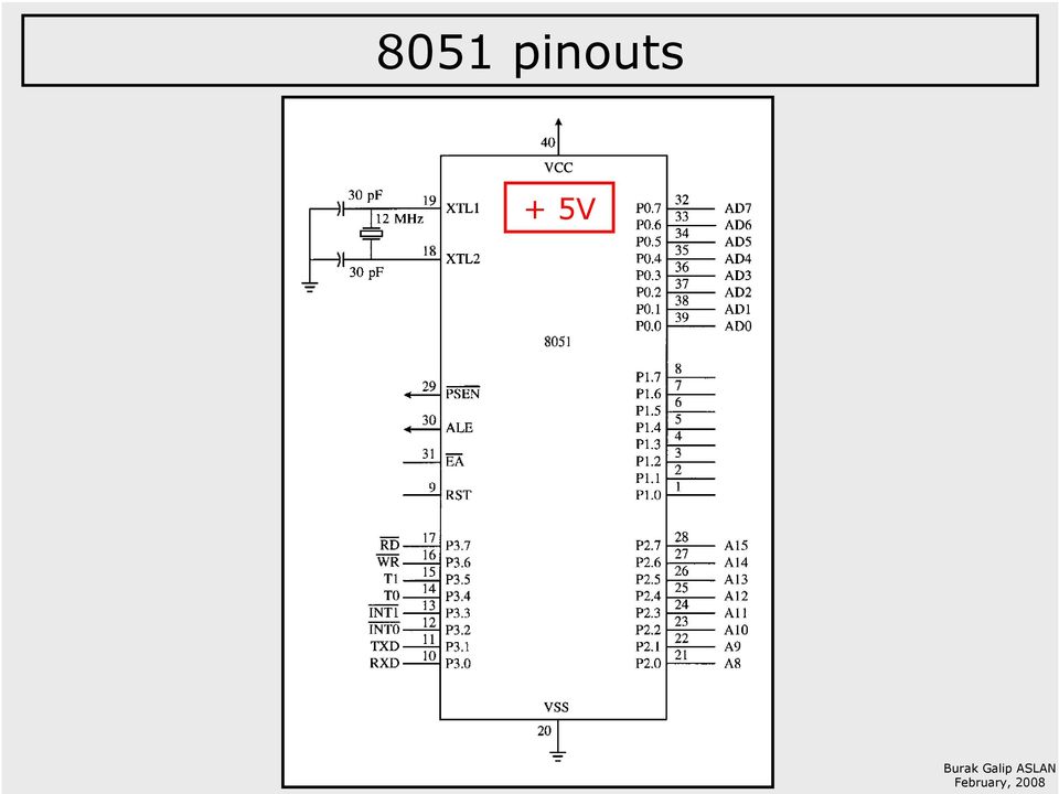
4 ports port 0 port 1 port 2 port 3 : dual-purpose (general-purpose, external memory address and data) : dedicated (interfacing to external devices) : dual-purpose (general-purpose, external memory address and data) : dual-purpose (general-purpose, special features)
 :")
5 port 3 special features

6 bus control signals PSEN ALE EA RST : Program Store Enable (enables external program memory) : Address Latch Enable (demultiplexing the address and data bus) : External Access (program execution from external or internal memory, programming of internal PEROM) : Reset (system start-up)
 : Reset")
7 on-chip oscillator inputs on-chip oscillator can either be driven by a crystal (~ 12 MHz) or a TTL clock source
 or a TTL")
8 I/O port structure 4 low-power Schottky TTL loads for ports 1, 2, 3 8 LS loads for Port 0

9 pull-up / pull-down resistors

10 TTL vs. CMOS Transistor-Transistor Logic BJTs (Bipolar Junction Transistor) + resistors low power consumption (more power consumption at rest, however it does not increase much with clock speed compared to CMOS) easier design rules slower Complementarysymmetry Metal-Oxide- Semiconductor MOSFETs (Metal-Oxide- Semiconductor Field- Effect-Transistors) high power consumption (it increases dramatically with clock speed) harder to design faster

11 TTL vs. CMOS (cont d) TTL NAND gate CMOS NAND gate

12 memory organization 128B internal RAM 4KB ROM can be expanded to 64KB code memory and 64KB data memory registers and I/O ports are memory-mapped and accessible like any other memory location stack resides within the internal RAM (unlike microprocessors using external RAM for stack)

13 internal RAM
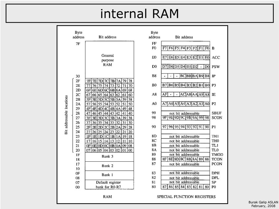
14 general-purpose RAM 80B MOV direct addressing A, 5FH MOV R0, #5FH MOV indirect addressing 00H 2FH can be used as similar (80B + 48B = 128B) any location in the general-purpose RAM can be accessed freely using direct and indirect addressing modes


15 bit-addressable RAM 210 bit-addressable locations individually accessing bits SETB 67H microcontroller MOV A, 2CH ORL A, # B MOV 2CH, A microprocessor

16 register banks PSW context-switching default by system reset MOV A, R5 register addressing 1B MOV A, 05H direct addressing 2B

")
17 Special Function Registers 21 SFRs some of them are both bitaddressable and byteaddressable SETB E0H E0H : bit-address of the accumulator E0H : byte-address of the accumulator P0 : 80H (80H 87H) {10000xxx}
")
18 Program Status Word
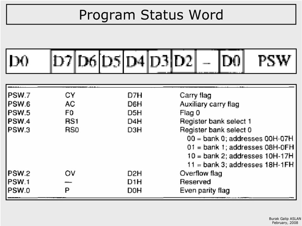
19 CarrY flag of PSW arithmetic operations boolean accumulator ADD A, #1 ; A = FFH ANL C, 25H CY is set result is stored in CY

20 Auxiliary Carry flag of PSW checks the lower nibble of result in BCD addition XXXX 1010 if {0AH OFH} AC is set DA A ; Decimal Adjust Accumulator (result back in range 9) DA must follow the addition
 DA must")
21 Flag 0 of PSW general-purpose flag bit, F0 (for user applications)
22 Register bank Select bits of PSW SETB SETB MOV RS1 RS0 A, R7
23 OVerflow flag of PSW when unsigned numbers are added or subtracted, OV can be ignored when signed numbers are added or subtracted, results out of {-128 to +127} sets OV
24 Parity bit of PSW P bit is automatically set or cleared with each machine cycle (even parity check on accumulator) if [number of 1 s in accumulator] + 1 = even then (P = 1)
25 B register MUL AB ; A(8-bit) X B(8-bit) = 16-bit result (high-byte, low-byte) DIV AB ; A(8-bit) / B(8-bit) = 8-bit integer result, 8-bit remainder it can also be used as a generalpurpose scratch-pad register
26 Stack Pointer 32B SS push -> first SP+1, then write data pop -> first read data, then SP-1 default by system reset : 07H MOV SP, #5FH ; beginning address of stack = 60H!!! be very careful of what you are doing if you do not initialize your own stack space but still use context switching, and PUSH, POP, ACALL, LCALL, RET, RETI instructions on stack space (SS)
27 Data PoinTeR high-byte - DPH low-byte - DPL accessing external code or external data memory MOV A, #55H ; immediate addressing MOV DPTR, #1000H ; immediate addressing A ; indirect addressing 55H
 are used P1.2 to P1.7 are always available for general purpose I/O lines WAIT: SETB P1.7 CLR P1.7 JB P1.5, WAIT 1 device busy 0 device ready")
28 Port registers ports 0,2 and 3 may not be available for I/O if external memory is used or if some 8051 special features (interrupts, serial ports, etc.) are used P1.2 to P1.7 are always available for general purpose I/O lines WAIT: SETB P1.7 CLR P1.7 JB P1.5, WAIT 1 device busy 0 device ready

29 Timer registers two 16-bit timer/counters high-byte TH1 high-byte TH0 low-byte TL1 low-byte TL0 Timer MODe register Timer CONtrol register Timer 0 : {TH0, TL0} Timer 1 : {TH1, TL1} only TCON is bit-addressable
30 Serial port registers on-chip serial port for communicating with serial devices Serial data BUFfer (SBUF) holds both the transmit data (writing to buffer) and the receive data (reading from buffer) Various modes of operation on bitaddressable Serial port CONtrol register (SCON)
 priority level is set through the Interrupt Priority register")
31 Interrupt registers 5-source, 2-priority level interrupt structure interrupts are disabled as default by system reset should be enabled by writing to the Interrupt Enable register (IE) priority level is set through the Interrupt Priority register (IP)
32 Power CONtrol register
33 IDLe mode an instruction that sets IDL bit will be the last instruction executed before entering idle mode CPU status preserved, all register contents are maintained port pins retain their logic levels ALE and PSEN are held high idle mode is terminated by any enabled interrupt or by system reset, either condition clears the IDL bit
34 Power Down mode an instruction that sets PD bit will be the last instruction executed before entering power down mode on-chip oscillator stopped all function are stopped all on-chip RAM contents are retained port pins retain their logic levels ALE and PSEN are held low only exit is system reset V CC can be as low as 2V in power down mode
35 external memory 64K external code memory space and 64K external data memory space can be made available by 8051 architecture when external memory is used P0 is unavaliable as an I/O port P0 becomes a multiplexed address (A0-A7) and data (D0-D7) bus with ALE latching the low-byte of the address at the beginning of each memory cycle if MOVX instructions are never used ALE pulses consistently at 1/6 of crystal frequency if MOVX instruction is used both ALE and PSEN pulses are skipped once on the RD line to enable the RAM
36 multiplexing address and data buses
37 accessing external code memory
38 read timing for external code memory
39 accessing external data memory
40 accessing external data memory (cont d) MOVX instruction MOVX SETB P2.0 SETB P2.1 MOV R0, #FFH MOVX read 03FFH
41 address decoding
42 external memory (cont d) increment RAM location by 1: it takes 1 instruction and 1 instruction cycles for internal RAM it takes 4 instructions and 7 instruction cycles for external RAM external memory is ~ 7 times slower size: internal RAM is limited to 128B external RAM up to 64KB
43 overlapping the external code and data spaces
44 von Neumann architecture stored program concept program can modify themselves on the run program faults can effect other programs, operating system leading to crash es memory protection and access control mechanisms against malware von Neumann bottleneck caches, branch prediction algorithms
45 Hardvard architecture separate storage and signal pathways for instructions and data modifying programs is entirely an offline process instruction memory often wider than data memory speed is gained at the expense of more complex electrical circuitry caches (high cost) for memory bound problem specialized DSPs (audio/video, etc.), small microcontrollers (PIC, etc.) modern high-performance CPU designs incorporate aspects of both von Neumann and Harvard architectures
46 ReSeT operation 8051 is reset by holding RST high for two machine cycles and then returning it low power-on reset manual reset
47 Register values after system ReSeT
48 summary 8051 architecture and layout memory organization Special Function Registers external memory
49 references
Flash Microcontroller. Memory Organization. Memory Organization
 The information presented in this chapter is collected from the Microcontroller Architectural Overview, AT89C51, AT89LV51, AT89C52, AT89LV52, AT89C2051, and AT89C1051 data sheets of this book. The material
8-Bit Flash Microcontroller for Smart Cards. AT89SCXXXXA Summary. Features. Description. Complete datasheet available under NDA
 Features Compatible with MCS-51 products On-chip Flash Program Memory Endurance: 1,000 Write/Erase Cycles On-chip EEPROM Data Memory Endurance: 100,000 Write/Erase Cycles 512 x 8-bit RAM ISO 7816 I/O Port
Flash Microcontroller. Architectural Overview. Features. Block Diagram. Figure 1. Block Diagram of the AT89C core
 Features 8-Bit CPU Optimized for Control Applications Extensive Boolean Processing Capabilities (Single-Bit Logic) On-Chip Flash Program Memory On-Chip Data RAM Bidirectional and Individually Addressable
Microcomputer Components SAB 80515/SAB 80C515 8-Bit Single-Chip Microcontroller Family
 Microcomputer Components SAB 80515/SAB 80C515 8-Bit Single-Chip Microcontroller Family User's Manual 08.95 SAB 80515 / SAB 80C515 Family Revision History: 8.95 Previous Releases: 12.90/10.92 Page Subjects
MICROPROCESSOR. Exclusive for IACE Students www.iace.co.in iacehyd.blogspot.in Ph: 9700077455/422 Page 1
 MICROPROCESSOR A microprocessor incorporates the functions of a computer s central processing unit (CPU) on a single Integrated (IC), or at most a few integrated circuit. It is a multipurpose, programmable
AT89C1051. 8-Bit Microcontroller with 1 Kbyte Flash. Features. Description. Pin Configuration
 AT89C1051 Features Compatible with MCS-51 Products 1 Kbyte of Reprogrammable Flash Memory Endurance: 1,000 Write/Erase Cycles 2.7 V to 6 V Operating Range Fully Static Operation: 0 Hz to 24 MHz Two-Level
PART B QUESTIONS AND ANSWERS UNIT I
 PART B QUESTIONS AND ANSWERS UNIT I 1. Explain the architecture of 8085 microprocessor? Logic pin out of 8085 microprocessor Address bus: unidirectional bus, used as high order bus Data bus: bi-directional
Cellphone Based Device Control With Voice Acknowledgement
 Cellphone Based Device Control With Voice Acknowledgement Avigyan Datta Gupta 1, Sayan Samanta 2, Avishek Acharjee 3 1,2 Future Institute of Engineering and Management, Kolkata-700150 3 Techno India, Kolkata-700150
CoE3DJ4 Digital Systems Design. Chapter 4: Timer operation
 CoE3DJ4 Digital Systems Design Chapter 4: Timer operation Timer There are two 16-bit timers each with four modes of operation Timers are used for (a) interval timing, (b) event counting or (c) baud rate
DEPARTMENT OF COMPUTER SCIENCE & ENGINEERING Question Bank Subject Name: EC6504 - Microprocessor & Microcontroller Year/Sem : II/IV
 DEPARTMENT OF COMPUTER SCIENCE & ENGINEERING Question Bank Subject Name: EC6504 - Microprocessor & Microcontroller Year/Sem : II/IV UNIT I THE 8086 MICROPROCESSOR 1. What is the purpose of segment registers
Hardware and Software Requirements
 C Compiler Real-Time OS Simulator Training Evaluation Boards Installing and Using the Keil Monitor-51 Application Note 152 May 31, 2000, Munich, Germany by Keil Support, Keil Elektronik GmbH [email protected]
DS87C520/DS83C520 EPROM/ROM High-Speed Micro
 www.maxim-ic.com PRELIMINARY EPROM/ROM High-Speed Micro FEATURES 80C52-compatible - 8051 pin and instruction set compatible - Four 8-bit I/O ports - Three 16-bit timer/counters - 256 bytes scratchpad RAM
Microtronics technologies Mobile: 99707 90092
 For more Project details visit: http://www.projectsof8051.com/rfid-based-attendance-management-system/ Code Project Title 1500 RFid Based Attendance System Synopsis for RFid Based Attendance System 1.
8031AH 8051AH 8032AH 8052AH NMOS SINGLE-CHIP 8-BIT MICROCONTROLLERS
 8031AH 8051AH 8032AH 8052AH MCS 51 NMOS SINGLE-CHIP 8-BIT MICROCONTROLLERS Automotive High Performance HMOS Process Internal Timers Event Counters 2-Level Interrupt Priority Structure 32 I O Lines (Four
8085 INSTRUCTION SET
 DATA TRANSFER INSTRUCTIONS Opcode Operand Description 8085 INSTRUCTION SET INSTRUCTION DETAILS Copy from source to destination OV Rd, Rs This instruction copies the contents of the source, Rs register
8051 Serial Port. Crystal TXD. I/O Device RXD. Embedded Systems 1 5-1 8051 Peripherals
 8051 Serial Port The 8051 contains a UART Universal Asynchronous Receiver Transmitter The serial port is full-duplex It can transmit and receive simultaneously 2 Port 3 pins are used to provide the serial
150127-Microprocessor & Assembly Language
 Chapter 3 Z80 Microprocessor Architecture The Z 80 is one of the most talented 8 bit microprocessors, and many microprocessor-based systems are designed around the Z80. The Z80 microprocessor needs an
MICROPROCESSOR AND MICROCOMPUTER BASICS
 Introduction MICROPROCESSOR AND MICROCOMPUTER BASICS At present there are many types and sizes of computers available. These computers are designed and constructed based on digital and Integrated Circuit
DS87C530/DS83C530. EPROM/ROM Micro with Real Time Clock PRELIMINARY FEATURES PACKAGE OUTLINE DALLAS DS87C530 DS83C530 DALLAS DS87C530 DS83C530
 PRELIMINARY DS87C530/DS83C530 EPROM/ROM Micro with Real Time Clock FEATURES 80C52 Compatible 8051 Instruction set compatible Four 8 bit I/O ports Three 16 bit timer/counters 256 bytes scratchpad RAM PACKAGE
MICROPROCESSOR BCA IV Sem MULTIPLE CHOICE QUESTIONS
 MICROPROCESSOR BCA IV Sem MULTIPLE CHOICE QUESTIONS 1) Which is the microprocessor comprises: a. Register section b. One or more ALU c. Control unit 2) What is the store by register? a. data b. operands
Keil C51 Cross Compiler
 Keil C51 Cross Compiler ANSI C Compiler Generates fast compact code for the 8051 and it s derivatives Advantages of C over Assembler Do not need to know the microcontroller instruction set Register allocation
8-bit Microcontroller with 8K Bytes In-System Programmable Flash. AT89LP52 - Preliminary
 Features 8-bit Microcontroller Compatible with 8051 Products Enhanced 8051 Architecture Single Clock Cycle per Byte Fetch 12 Clock per Machine Cycle Compatibility Mode Up to 20 MIPS Throughput at 20 MHz
AN108 IMPLEMENTING A REALTIME CLOCK. Relevant Devices. Introduction. Key Points. Overview
 IMPLEMENTING A REALTIME CLOCK Relevant Devices This application note applies to the following devices: C8051F000, C8051F001, C8051F002, C8051F005, C8051F006, C8051F007, C8051F010, C8051F011, and C8051F012.
Serial Communications
 Serial Communications 1 Serial Communication Introduction Serial communication buses Asynchronous and synchronous communication UART block diagram UART clock requirements Programming the UARTs Operation
8-bit Microcontroller with 2/4-Kbyte Flash AT89LP2052 AT89LP4052
 Features Compatible with MCS 51 Products 20 MIPS Throughput at 20 MHz Clock Frequency and 2.4V, 85 C Operating Conditions Single Clock Cycle per Byte Fetch 2/4K Bytes of In-System Programmable (ISP) Flash
MACHINE ARCHITECTURE & LANGUAGE
 in the name of God the compassionate, the merciful notes on MACHINE ARCHITECTURE & LANGUAGE compiled by Jumong Chap. 9 Microprocessor Fundamentals A system designer should consider a microprocessor-based
CpE358/CS381. Switching Theory and Logical Design. Class 4
 Switching Theory and Logical Design Class 4 1-122 Today Fundamental concepts of digital systems (Mano Chapter 1) Binary codes, number systems, and arithmetic (Ch 1) Boolean algebra (Ch 2) Simplification
8051 MICROCONTROLLER COURSE
 8051 MICROCONTROLLER COURSE Objective: 1. Familiarization with different types of Microcontroller 2. To know 8051 microcontroller in detail 3. Programming and Interfacing 8051 microcontroller Prerequisites:
4 Character 5x7 LED Matrix Display
 Mini project report on 4 Character 5x7 LED Matrix Display Submitted by Agarwal Vikas, MTech II, CEDT K.Sreenivasulu M.E (Micro) II, CEDT CENTRE FOR ELECTRONICS DESIGN AND TECHNOLOGY INDIAN INSTITUTE OF
UMBC. ISA is the oldest of all these and today s computers still have a ISA bus interface. in form of an ISA slot (connection) on the main board.
 on the main board.") Bus Interfaces Different types of buses: ISA (Industry Standard Architecture) EISA (Extended ISA) VESA (Video Electronics Standards Association, VL Bus) PCI (Periheral Component Interconnect) USB (Universal
Bus Interfaces Different types of buses: ISA (Industry Standard Architecture) EISA (Extended ISA) VESA (Video Electronics Standards Association, VL Bus) PCI (Periheral Component Interconnect) USB (Universal
HT1632C 32 8 &24 16 LED Driver
 328 &216 LED Driver Features Operating voltage: 2.V~5.5V Multiple LED display 32 ROW /8 COM and 2 ROW & 16 COM Integrated display RAM select 32 ROW & 8 COM for 6 display RAM, or select 2 ROW & 16 COM for
8XC51FX CHMOS SINGLE-CHIP 8-BIT MICROCONTROLLERS
 CHMOS SINGLE-CHIP 8-BIT MICROCONTROLLERS Commercial Express 87C51FA 83C51FA 80C51FA 87C51FB 83C51FB 87C51FC 83C51FC See Table 1 for Proliferation Options High Performance CHMOS EPROM ROM CPU 12 24 33 MHz
Develop a Dallas 1-Wire Master Using the Z8F1680 Series of MCUs
 Develop a Dallas 1-Wire Master Using the Z8F1680 Series of MCUs AN033101-0412 Abstract This describes how to interface the Dallas 1-Wire bus with Zilog s Z8F1680 Series of MCUs as master devices. The Z8F0880,
Embedded. Engineer s. Development. Tool (EEDT 5.0)
") Embedded Engineer s Development Tool (EEDT 5.0) User Manual and Tutorial Handbook DeccanRobots Developed and Distributed by DeccanRobots As a part of Embedded Engineer s Development Tool 5.0 www.deccanrobots.com
Embedded Engineer s Development Tool (EEDT 5.0) User Manual and Tutorial Handbook DeccanRobots Developed and Distributed by DeccanRobots As a part of Embedded Engineer s Development Tool 5.0 www.deccanrobots.com
Advanced Microcontrollers Grzegorz Budzyń Lecture. 3: Electrical parameters of microcontrollers 8051 family
 Advanced Microcontrollers Grzegorz Budzyń Lecture 3: Electrical parameters of microcontrollers 8051 family Plan Electrical parameters of microcontrollers 8051 core(8-bit) Main features 8051 based microcontrollers
SECTION C [short essay] [Not to exceed 120 words, Answer any SIX questions. Each question carries FOUR marks] 6 x 4=24 marks
![SECTION C [short essay] [Not to exceed 120 words, Answer any SIX questions. Each question carries FOUR marks] 6 x 4=24 marks](/thumbs/35/17285180.jpg "SECTION C [short essay] [Not to exceed 120 words, Answer any SIX questions. Each question carries FOUR marks] 6 x 4=24 marks") UNIVERSITY OF KERALA First Degree Programme in Computer Applications Model Question Paper Semester I Course Code- CP 1121 Introduction to Computer Science TIME : 3 hrs Maximum Mark: 80 SECTION A [Very
UNIVERSITY OF KERALA First Degree Programme in Computer Applications Model Question Paper Semester I Course Code- CP 1121 Introduction to Computer Science TIME : 3 hrs Maximum Mark: 80 SECTION A [Very
Instruction Set. Microcontroller Instruction Set. Instructions that Affect Flag Settings (1) The Instruction Set and Addressing Modes
 The Instruction Set and Addressing Modes") Microcontroller For interrupt response time information, refer to the hardware description chapter. Instructions that ffect Flag Settings (1) Instruction Flag Instruction Flag C OV C C OV C DD X X X CLR
Microcontroller For interrupt response time information, refer to the hardware description chapter. Instructions that ffect Flag Settings (1) Instruction Flag Instruction Flag C OV C C OV C DD X X X CLR
Z80 Microprocessors Z80 CPU. User Manual UM008006-0714. Copyright 2014 Zilog, Inc. All rights reserved. www.zilog.com
 Z80 Microprocessors Z80 CPU UM008006-0714 Copyright 2014 Zilog, Inc. All rights reserved. www.zilog.com ii Warning: DO NOT USE THIS PRODUCT IN LIFE SUPPORT SYSTEMS. LIFE SUPPORT POLICY ZILOG S PRODUCTS
Monitoring of Intravenous Drip Rate
 Monitoring of Intravenous Drip Rate Vidyadhar V. Kamble, Prem C. Pandey, Chandrashekar P. Gadgil, and Dinesh S. Choudhary Abstract A drip rate meter, for monitoring intravenous infusion, is developed using
Technical Note. Micron NAND Flash Controller via Xilinx Spartan -3 FPGA. Overview. TN-29-06: NAND Flash Controller on Spartan-3 Overview
 Technical Note TN-29-06: NAND Flash Controller on Spartan-3 Overview Micron NAND Flash Controller via Xilinx Spartan -3 FPGA Overview As mobile product capabilities continue to expand, so does the demand
8085 MICROPROCESSOR PROGRAMS
 8085 MICROPROCESSOR PROGRAMS 1 ADDITION OF TWO 8 BIT NUMBERS AIM: To perform addition of two 8 bit numbers using 8085. ALGORITHM: 1) Start the program by loading the first data into Accumulator. 2) Move
CHAPTER 7: The CPU and Memory
 CHAPTER 7: The CPU and Memory The Architecture of Computer Hardware, Systems Software & Networking: An Information Technology Approach 4th Edition, Irv Englander John Wiley and Sons 2010 PowerPoint slides
TDA8029. 1. General description. 2. Features and benefits. Low power single card reader
 Rev. 3.3 19 July 2016 Product data sheet 1. General description The is a complete one chip, low cost, low power, robust smart card reader. Its different power reduction modes and its wide supply voltage
8741A UNIVERSAL PERIPHERAL INTERFACE 8-BIT MICROCOMPUTER
 UNIVERSAL PERIPHERAL INTERFACE 8-BIT MICROCOMPUTER 8-Bit CPU plus ROM RAM I O Timer and Clock in a Single Package One 8-Bit Status and Two Data Registers for Asynchronous Slave-to- Master Interface DMA
Interrupts. 1.Maskable interrupt request can be ignored or delayed by the microprocessor and used in telephone
 Interrupts The interrupt I/O is a process of data transfer where-by an external device or a peripheral can inform the microprocessor that it is ready for communication The interrupt requests are classified
Faculty of Engineering Student Number:
 Philadelphia University Student Name: Faculty of Engineering Student Number: Dept. of Computer Engineering Final Exam, First Semester: 2012/2013 Course Title: Microprocessors Date: 17/01//2013 Course No:
Atmel 8051 Microcontrollers Hardware Manual
 Atmel 8051 Microcontrollers Hardware Manual Table of Contents Section 1 The 8051 Instruction Set... 1-2 1.1 Program Status Word...1-2 1.2 Addressing Modes...1-3 1.3 Arithmetic Instructions...1-5 1.4 Logical
DS18B20 Programmable Resolution 1-Wire Digital Thermometer
 www.dalsemi.com FEATURES Unique 1-Wire interface requires only one port pin for communication Multidrop capability simplifies distributed temperature sensing applications Requires no external components
8-bit Microcontroller with 12K Bytes Flash and 2K Bytes EEPROM AT89S8253
 Features Compatible with MCS -51 Products 12K Bytes of In-System Programmable (ISP) Flash Program Memory SPI Serial Interface for Program Downloading Endurance: 10,000 Write/Erase Cycles 2K Bytes EEPROM
Data Cables. Schmitt TTL LABORATORY ELECTRONICS II
 Data Cables Data cables link one instrument to another. Signals can attenuate or disperse on long wires. A direct wire works best for short cables of less than 10 ft. A TTL cable connection can use a Schmitt
PACKAGE OUTLINE DALLAS DS2434 DS2434 GND. PR 35 PACKAGE See Mech. Drawings Section
 PRELIMINARY DS2434 Battery Identification Chip FEATURES Provides unique ID number to battery packs PACKAGE OUTLINE Eliminates thermistors by sensing battery temperature on chip DALLAS DS2434 1 2 3 256
Allows the user to protect against inadvertent write operations. Device select and address bytes are Acknowledged Data Bytes are not Acknowledged
 Write Protect CAT24WCxxx I 2 C Serial EEPROMs. Allows the user to protect against inadvertent write operations. WP = V CC : Write Protected Device select and address bytes are Acknowledged Data Bytes are
DS1307ZN. 64 x 8 Serial Real-Time Clock
 DS137 64 x 8 Serial Real-Time Clock www.maxim-ic.com FEATURES Real-time clock (RTC) counts seconds, minutes, hours, date of the month, month, day of the week, and year with leap-year compensation valid
CSE2102 Digital Design II - Topics CSE2102 - Digital Design II
 CSE2102 Digital Design II - Topics CSE2102 - Digital Design II 6 - Microprocessor Interfacing - Memory and Peripheral Dr. Tim Ferguson, Monash University. AUSTRALIA. Tel: +61-3-99053227 FAX: +61-3-99053574
8-bit Microcontroller with 8K Bytes In-System Programmable Flash AT89S52
 Features Compatible with MCS -51 Products 8K Bytes of In-System Programmable (ISP) Flash Memory Endurance: 10,000 Write/Erase Cycles 4.0V to 5.5V Operating Range Fully Static Operation: 0 Hz to 33 MHz
7a. System-on-chip design and prototyping platforms
 7a. System-on-chip design and prototyping platforms Labros Bisdounis, Ph.D. Department of Computer and Communication Engineering 1 What is System-on-Chip (SoC)? System-on-chip is an integrated circuit
Chapter 1 Computer System Overview
 Operating Systems: Internals and Design Principles Chapter 1 Computer System Overview Eighth Edition By William Stallings Operating System Exploits the hardware resources of one or more processors Provides
AN141 SMBUS COMMUNICATION FOR SMALL FORM FACTOR DEVICE FAMILIES. 1. Introduction. 2. Overview of the SMBus Specification. 2.1.
 SMBUS COMMUNICATION FOR SMALL FORM FACTOR DEVICE FAMILIES 1. Introduction C8051F3xx and C8051F41x devices are equipped with an SMBus serial I/O peripheral that is compliant with both the System Management
The Programming Interface
 : In-System Programming Features Program any AVR MCU In-System Reprogram both data Flash and parameter EEPROM memories Eliminate sockets Simple -wire SPI programming interface Introduction In-System programming
C167Derivatives 16-Bit CMOS Single-Chip Microcontrollers. User's Manual 03.96 Version 2.0 http://www.siemens.de/ Semiconductor/
 C167Derivatives 16-Bit CMOS Single-Chip Microcontrollers User's Manual 03.96 Version 2.0 http://www.siemens.de/ Semiconductor/ C167 Revision History: Version 2.0 (03.96) Previous Version: Version 1.0 (08.94)
(Refer Slide Time: 00:01:16 min)
") Digital Computer Organization Prof. P. K. Biswas Department of Electronic & Electrical Communication Engineering Indian Institute of Technology, Kharagpur Lecture No. # 04 CPU Design: Tirning & Control
Digital Computer Organization Prof. P. K. Biswas Department of Electronic & Electrical Communication Engineering Indian Institute of Technology, Kharagpur Lecture No. # 04 CPU Design: Tirning & Control
DS1821 Programmable Digital Thermostat and Thermometer
 ma www.maxim-ic.com FEATURES Requires no external components Unique 1-Wire interface requires only one port pin for communication Operates over a -55 C to +125 C (67 F to +257 F) temperature range Functions
ELEG3924 Microprocessor Ch.7 Programming In C
 Department of Electrical Engineering University of Arkansas ELEG3924 Microprocessor Ch.7 Programming In C Dr. Jingxian Wu [email protected] OUTLINE 2 Data types and time delay I/O programming and Logic operations
Learning Outcomes. Simple CPU Operation and Buses. Composition of a CPU. A simple CPU design
 Learning Outcomes Simple CPU Operation and Buses Dr Eddie Edwards [email protected] At the end of this lecture you will Understand how a CPU might be put together Be able to name the basic components
Am186ER/Am188ER AMD Continues 16-bit Innovation
 Am186ER/Am188ER AMD Continues 16-bit Innovation 386-Class Performance, Enhanced System Integration, and Built-in SRAM Problem with External RAM All embedded systems require RAM Low density SRAM moving
24-Bit Analog-to-Digital Converter (ADC) for Weigh Scales FEATURES S8550 VFB. Analog Supply Regulator. Input MUX. 24-bit Σ ADC. PGA Gain = 32, 64, 128
 for Weigh Scales FEATURES S8550 VFB. Analog Supply Regulator. Input MUX. 24-bit Σ ADC. PGA Gain = 32, 64, 128") 24-Bit Analog-to-Digital Converter (ADC) for Weigh Scales DESCRIPTION Based on Avia Semiconductor s patented technology, HX711 is a precision 24-bit analogto-digital converter (ADC) designed for weigh
24-Bit Analog-to-Digital Converter (ADC) for Weigh Scales DESCRIPTION Based on Avia Semiconductor s patented technology, HX711 is a precision 24-bit analogto-digital converter (ADC) designed for weigh
Chapter 1 Lesson 3 Hardware Elements in the Embedded Systems. 2008 Chapter-1L03: "Embedded Systems - ", Raj Kamal, Publs.: McGraw-Hill Education
 Chapter 1 Lesson 3 Hardware Elements in the Embedded Systems 1 Typical Embedded System Hardware units 2 Basic Circuit Elements at the System 3 (i) Power Source 1. System own supply with separate supply
Introduction. What is an Operating System?
 Introduction What is an Operating System? 1 What is an Operating System? 2 Why is an Operating System Needed? 3 How Did They Develop? Historical Approach Affect of Architecture 4 Efficient Utilization
64 x 8, Serial, I 2 C Real-Time Clock
 DS1307 64 x 8, Serial, I 2 C Real-Time Clock GENERAL DESCRIPTION The DS1307 serial real-time clock (RTC) is a lowpower, full binary-coded decimal (BCD) clock/calendar plus 56 bytes of NV SRAM. Address
Chapter 5, The Instruction Set Architecture Level
 Chapter 5, The Instruction Set Architecture Level 5.1 Overview Of The ISA Level 5.2 Data Types 5.3 Instruction Formats 5.4 Addressing 5.5 Instruction Types 5.6 Flow Of Control 5.7 A Detailed Example: The
W25Q80, W25Q16, W25Q32 8M-BIT, 16M-BIT AND 32M-BIT SERIAL FLASH MEMORY WITH DUAL AND QUAD SPI
 8M-BIT, 16M-BIT AND 32M-BIT SERIAL FLASH MEMORY WITH DUAL AND QUAD SPI - 1 - Preliminary - Revision B Table of Contents 1. GENERAL DESCRIPTION... 5 2. FEATURES... 5 3. PIN CONFIGURATION SOIC 208-MIL...
Microcontroller Basics A microcontroller is a small, low-cost computer-on-a-chip which usually includes:
 Microcontroller Basics A microcontroller is a small, low-cost computer-on-a-chip which usually includes: An 8 or 16 bit microprocessor (CPU). A small amount of RAM. Programmable ROM and/or flash memory.
CHAPTER 4 MARIE: An Introduction to a Simple Computer
 CHAPTER 4 MARIE: An Introduction to a Simple Computer 4.1 Introduction 195 4.2 CPU Basics and Organization 195 4.2.1 The Registers 196 4.2.2 The ALU 197 4.2.3 The Control Unit 197 4.3 The Bus 197 4.4 Clocks
Chapter 2 Logic Gates and Introduction to Computer Architecture
 Chapter 2 Logic Gates and Introduction to Computer Architecture 2.1 Introduction The basic components of an Integrated Circuit (IC) is logic gates which made of transistors, in digital system there are
Chapter 13. PIC Family Microcontroller
 Chapter 13 PIC Family Microcontroller Lesson 01 PIC Characteristics and Examples PIC microcontroller characteristics Power-on reset Brown out reset Simplified instruction set High speed execution Up to
Digitale Signalverarbeitung mit FPGA (DSF) Soft Core Prozessor NIOS II Stand Mai 2007. Jens Onno Krah
 Soft Core Prozessor NIOS II Stand Mai 2007. Jens Onno Krah") (DSF) Soft Core Prozessor NIOS II Stand Mai 2007 Jens Onno Krah Cologne University of Applied Sciences www.fh-koeln.de [email protected] NIOS II 1 1 What is Nios II? Altera s Second Generation
(DSF) Soft Core Prozessor NIOS II Stand Mai 2007 Jens Onno Krah Cologne University of Applied Sciences www.fh-koeln.de [email protected] NIOS II 1 1 What is Nios II? Altera s Second Generation
Real-Time Clock. * Real-Time Computing, edited by Duncan A. Mellichamp, Van Nostrand Reinhold
 REAL-TIME CLOCK Real-Time Clock The device is not a clock! It does not tell time! It has nothing to do with actual or real-time! The Real-Time Clock is no more than an interval timer connected to the computer
Microcontroller Based Low Cost Portable PC Mouse and Keyboard Tester
 Leonardo Journal of Sciences ISSN 1583-0233 Issue 20, January-June 2012 p. 31-36 Microcontroller Based Low Cost Portable PC Mouse and Keyboard Tester Ganesh Sunil NHIVEKAR *, and Ravidra Ramchandra MUDHOLKAR
Content Map For Career & Technology
 Content Strand: Applied Academics CT-ET1-1 analysis of electronic A. Fractions and decimals B. Powers of 10 and engineering notation C. Formula based problem solutions D. Powers and roots E. Linear equations
DS1621 Digital Thermometer and Thermostat
 Digital Thermometer and Thermostat www.dalsemi.com FEATURES Temperature measurements require no external components Measures temperatures from 55 C to +125 C in 0.5 C increments. Fahrenheit equivalent
1 Gbit, 2 Gbit, 4 Gbit, 3 V SLC NAND Flash For Embedded
 1 Gbit, 2 Gbit, 4 Gbit, 3 V SLC NAND Flash For Embedded Distinctive Characteristics Density 1 Gbit / 2 Gbit / 4 Gbit Architecture Input / Output Bus Width: 8-bits / 16-bits Page Size: x8 = 2112 (2048 +
Hello, and welcome to this presentation of the STM32L4 reset and clock controller.
 Hello, and welcome to this presentation of the STM32L4 reset and clock controller. 1 The STM32L4 reset and clock controller manages system and peripheral clocks. STM32L4 devices embed three internal oscillators,
Low Power AMD Athlon 64 and AMD Opteron Processors
 Low Power AMD Athlon 64 and AMD Opteron Processors Hot Chips 2004 Presenter: Marius Evers Block Diagram of AMD Athlon 64 and AMD Opteron Based on AMD s 8 th generation architecture AMD Athlon 64 and AMD
Z80 Instruction Set. Z80 Assembly Language
 75 Z80 Assembly Language The assembly language allows the user to write a program without concern for memory addresses or machine instruction formats. It uses symbolic addresses to identify memory locations
8-bit Flash Microcontroller with 64K bytes Program Memory AT89LP51RD2 AT89LP51ED2 AT89LP51ID2
 Features 8-bit Microcontroller Compatible with 8051 Products Enhanced 8051 Architecture Single Clock Cycle per Byte Fetch 12 Clock per Machine Cycle Compatibility Mode Up to 20 MIPS Throughput at 20 MHz
CPU Organisation and Operation
 CPU Organisation and Operation The Fetch-Execute Cycle The operation of the CPU 1 is usually described in terms of the Fetch-Execute cycle. 2 Fetch-Execute Cycle Fetch the Instruction Increment the Program
Small Hardware Development and Prototyping Board for the SX28
 Project Report: Small Hardware Development and Prototyping Board for the SX28 Project Number: PR57 1. Project Description 2. Schematic Diagram 3. Physical Diagram 4. Component Layout Diagram 5. Bill of
Design Analysis of a Security Lock System using Pass-Code and Smart-Card
 IOSR Journal of Electronics and Communication Engineering (IOSR-JECE) e-issn: 2278-2834, p- ISSN: 2278-8735. Volume 4, Issue 6 (Jan. - Feb. 2013), PP 64-72 Design Analysis of a Security Lock System using
Computer-System Architecture
 Chapter 2: Computer-System Structures Computer System Operation I/O Structure Storage Structure Storage Hierarchy Hardware Protection General System Architecture 2.1 Computer-System Architecture 2.2 Computer-System
DP8570A DP8570A Timer Clock Peripheral (TCP)
") DP8570A DP8570A Timer Clock Peripheral (TCP) Literature Number: SNAS557 DP8570A Timer Clock Peripheral (TCP) General Description The DP8570A is intended for use in microprocessor based systems where information
DP8570A DP8570A Timer Clock Peripheral (TCP) Literature Number: SNAS557 DP8570A Timer Clock Peripheral (TCP) General Description The DP8570A is intended for use in microprocessor based systems where information
Interfacing To Alphanumeric Displays
 Interfacing To Alphanumeric Displays To give directions or data values to users, many microprocessor-controlled instruments and machines need to display letters of the alphabet and numbers. In systems
PIN ASSIGNMENT. www.dalsemi.com 64-PIN QFP
 www.dalsemi.com PRELIMINARY Dual CAN High-Speed Microprocessor FEATURES 80C52 compatible 8051 instruction-set compatible Four 8-bit I/O ports Three 16-bit timer/counters 256 bytes scratchpad RAM High-Speed
ARM Thumb Microcontrollers. Application Note. Software ISO 7816 I/O Line Implementation. Features. Introduction
 Software ISO 7816 I/O Line Implementation Features ISO 7816-3 compliant (direct convention) Byte reception and transmission with parity check Retransmission on error detection Automatic reception at the
Introduction to Microcontrollers
 Introduction to Microcontrollers Motorola M68HC11 Specs Assembly Programming Language BUFFALO Topics of Discussion Microcontrollers M68HC11 Package & Pinouts Accumulators Index Registers Special Registers
DS12887. Real Time Clock FEATURES PIN ASSIGNMENT PIN DESCRIPTION
 DS12887 Real Time Clock FEATURES Drop in replacement for IBM AT computer clock/ calendar Pin compatible with the MC146818B and DS1287 Totally nonvolatile with over 10 years of operation in the absence
TURBO PROGRAMMER USB, MMC, SIM DEVELOPMENT KIT
 TURBO PROGRAMMER USB, MMC, SIM DEVELOPMENT KIT HARDWARE GUIDE This document is part of Turbo Programmer documentation. For Developer Documentation, Applications and Examples, see http:/// PRELIMINARY (C)
Module 2. Embedded Processors and Memory. Version 2 EE IIT, Kharagpur 1
 Module 2 Embedded Processors and Memory Version 2 EE IIT, Kharagpur 1 Lesson 5 Memory-I Version 2 EE IIT, Kharagpur 2 Instructional Objectives After going through this lesson the student would Pre-Requisite
Interfacing Analog to Digital Data Converters
 Converters In most of the cases, the PIO 8255 is used for interfacing the analog to digital converters with microprocessor. We have already studied 8255 interfacing with 8086 as an I/O port, in previous
The I2C Bus. NXP Semiconductors: UM10204 I2C-bus specification and user manual. 14.10.2010 HAW - Arduino 1
 The I2C Bus Introduction The I2C-bus is a de facto world standard that is now implemented in over 1000 different ICs manufactured by more than 50 companies. Additionally, the versatile I2C-bus is used
8-bit Microcontroller with 2K Bytes Flash AT89C2051
 Features Compatible with MCS -51Products 2K Bytes of Reprogrammable Flash Memory Endurance: 10,000 Write/Erase Cycles 2.7V to 6V Operating Range Fully Static Operation: 0 Hz to 24 MHz Two-level Program