S-57M1 Series HIGH-SPEED BIPOLAR HALL EFFECT LATCH. Features. Applications. Package.
|
|
|
- Brett Stewart
- 9 years ago
- Views:
Transcription
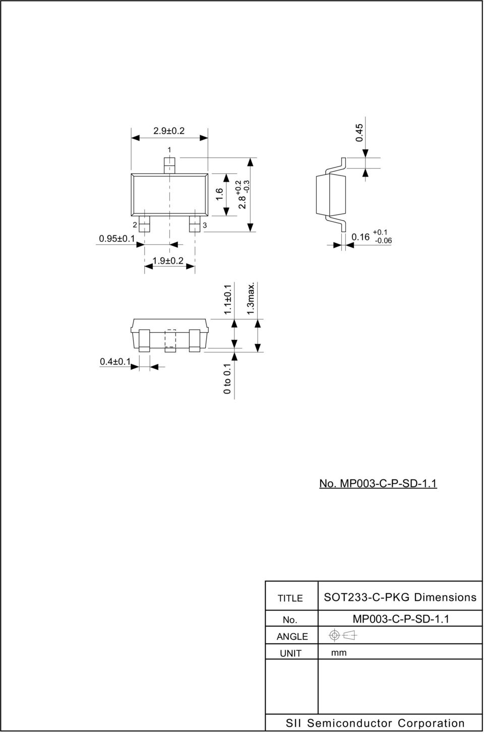
1 HIGH-SPEED BIPOLAR HALL EFFECT LATCH SII Semiconductor Corporation, Rev.1.2_01 The, developed by CMOS technology, is a high-accuracy Hall IC that operates with a high-sensitivity, a high-speed detection and low current consumption. The output voltage changes when the detects the intensity level of magnetic flux density and a polarity change. Using the with a magnet makes it possible to detect the rotation status in various devices. High-density mounting is possible by using the small SOT-23-3 package. Due to its high-accuracy magnetic characteristics, the can make operation s dispersion in the system combined with magnet smaller. Caution This product is intended to use in general electronic devices such as consumer electronics, office equipment, and communications devices. Before using the product in medical equipment or automobile equipment including car audio, keyless entry and engine control unit, contact to SII Semiconductor Corporation is indispensable. Features Pole detection: Detection logic for magnetism *1 : Output form *1 : Magnetic sensitivity: Operation cycle (current consumption): Power supply voltage range: Operation temperature range: Lead-free (Sn 100%), halogen-free *2 Bipolar latch VOUT = "L" at S pole detection VOUT = "H" at S pole detection Nch open-drain output, CMOS output BOP = 3.0 mt typ. tcycle = 50 μs (1400 μa) typ. VDD = 2.7 V to 5.5 V Ta = 40 C to +125 C *1. The option can be selected. *2. Refer to " Product Name Structure" for details. Applications Motor Housing equipment Industrial equipment Package SOT

2 HIGH-SPEED BIPOLAR HALL EFFECT LATCH Rev.1.2_01 Block Diagrams 1. Nch open-drain output product VDD OUT *1 *1 Chopping stabilized amplifier VSS *1. Parasitic diode Figure 1 2. CMOS output product VDD *1 *1 OUT VSS Chopping stabilized amplifier *1 *1. Parasitic diode Figure 2 2

3 Rev.1.2_01 HIGH-SPEED BIPOLAR HALL EFFECT LATCH Product Name Structure 1. Product name S-57M1 x B x 1 B - M3T1 U Environmental code U: Lead-free (Sn 100%), halogen-free Package name (abbreviation) and packing specifications *1 M3T1: SOT-23-3, Tape Operation temperature B: Ta = 40 C to +125 C Magnetic sensitivity 1: B OP = 3.0 mt typ. Detection logic for magnetism L: V OUT = "L" at S pole detection H: V OUT = "H" at S pole detection Pole detection B: Bipolar latch Output form N: Nch open-drain output C: CMOS output *1. Refer to the tape drawing. 2. Package Table 1 Package Drawing Codes Package Name Dimension Tape Reel SOT-23-3 MP003-C-P-SD MP003-C-C-SD MP003-Z-R-SD 3. Product name list Table 2 Detection Logic Product Name Output Form Pole Detection for Magnetism VOUT = "L" at S pole S-57M1NBL1B-M3T1U Nch open-drain output Bipolar latch detection VOUT = "H" at S pole S-57M1NBH1B-M3T1U Nch open-drain output Bipolar latch detection VOUT = "H" at S pole S-57M1CBH1B-M3T1U CMOS output Bipolar latch detection Remark Please contact our sales office for products other than the above. Magnetic Sensitivity (BOP) 3.0 mt typ. 3.0 mt typ. 3.0 mt typ. 3

4 HIGH-SPEED BIPOLAR HALL EFFECT LATCH Rev.1.2_01 Pin Configuration 1. SOT-23-3 Top view Table 3 Pin No. Symbol Description 1 VSS GND pin 2 VDD Power supply pin 3 OUT Output pin Figure 3 Absolute Maximum Ratings Table 4 (Ta = +25 C unless otherwise specified) Item Symbol Absolute Maximum Rating Unit Power supply voltage VDD VSS 0.3 to VSS V Output current IOUT ±2.0 ma Nch open-drain output Output voltage product VOUT VSS 0.3 to VSS V CMOS output product VSS 0.3 to VDD V Power dissipation PD 430 *1 mw Operation ambient temperature Topr 40 to +125 C Storage temperature Tstg 40 to +150 C *1. When mounted on board [Mounted board] (1) Board size: mm 76.2 mm t1.6 mm (2) Name: JEDEC STANDARD51-7 Caution The absolute maximum ratings are rated values exceeding which the product could suffer physical damage. These values must therefore not be exceeded under any conditions. 4
 Board size: 114.3 mm 76.2 mm t1.")
5 Rev.1.2_01 HIGH-SPEED BIPOLAR HALL EFFECT LATCH Electrical Characteristics Table 5 (Ta = +25 C, VDD = 5.0 V, VSS = 0 V unless otherwise specified) Item Symbol Condition Min. Typ. Max. Unit Power supply voltage VDD V Current consumption IDD Average value μa 1 Output voltage VOUT Nch open-drain output product CMOS output product Output transistor Nch, IOUT = 2 ma Output transistor Nch, IOUT = 2 ma Output transistor Pch, IOUT = 2 ma Test Circuit 0.4 V V 2 VDD 0.4 V 3 Leakage current ILEAK Nch open-drain output product Output transistor Nch, VOUT = 5.5 V 1 μa 4 Operation cycle tcycle μs Magnetic Characteristics Table 6 (Ta = +25 C, VDD = 5.0 V, VSS = 0 V unless otherwise specified) Item Symbol Condition Min. Typ. Max. Unit Test Circuit Operation point *1 S pole BOP mt 5 Release point *2 N pole BRP mt 5 Hysteresis width *3 BHYS BHYS = BOP BRP 6.0 mt 5 *1. BOP: Operation point BOP is the value of magnetic flux density when the output voltage (VOUT) changes after the magnetic flux density applied to the by the magnet (S pole) is increased (by moving the magnet closer). VOUT retains the status until a magnetic flux density of the N pole higher than BRP is applied. *2. BRP: Release point BRP is the value of magnetic flux density when the output voltage (VOUT) changes after the magnetic flux density applied to the by the magnet (N pole) is increased (by moving the magnet closer). VOUT retains the status until a magnetic flux density of the S pole higher than BOP is applied. *3. BHYS: Hysteresis width BHYS is the difference of magnetic flux density between BOP and BRP. Remark The unit of magnetic density mt can be converted by using the formula 1 mt = 10 Gauss. 5

6 HIGH-SPEED BIPOLAR HALL EFFECT LATCH Rev.1.2_01 Test Circuits A R *1 100 kω VDD S-57M1 Series OUT VSS *1. Resistor (R) is unnecessary for the CMOS output product. Figure 4 Test Circuit 1 VDD S-57M1 Series OUT VSS V A Figure 5 Test Circuit 2 VDD S-57M1 Series OUT VSS V A Figure 6 Test Circuit 3 6

7 Rev.1.2_01 HIGH-SPEED BIPOLAR HALL EFFECT LATCH VDD S-57M1 Series OUT VSS V A Figure 7 Test Circuit 4 R *1 100 kω VDD S-57M1 Series OUT VSS V *1. Resistor (R) is unnecessary for the CMOS output product. Figure 8 Test Circuit 5 7

8 HIGH-SPEED BIPOLAR HALL EFFECT LATCH Rev.1.2_01 Standard Circuit C IN 0.1 μf VDD S-57M1 Series OUT VSS R *1 100 kω *1. Resistor (R) is unnecessary for the CMOS output product. Figure 9 Caution The above connection diagram and constant will not guarantee successful operation. Perform thorough evaluation using the actual application to set the constant. 8

9 Rev.1.2_01 HIGH-SPEED BIPOLAR HALL EFFECT LATCH Operation 1. Direction of applied magnetic flux The detects the magnetic flux density which is vertical to the marking surface. Figure 10 shows the direction in which magnetic flux is being applied. N S Marking surface Figure Position of Hall sensor Figure 11 shows the position of Hall sensor. The center of this Hall sensor is located in the area indicated by a circle, which is in the center of a package as described below. The following also shows the distance (typ. value) between the marking surface and the chip surface of a package. Top view 1 The center of Hall sensor; in this φ 0.3 mm mm (typ.) Figure 11 9

10 HIGH-SPEED BIPOLAR HALL EFFECT LATCH Rev.1.2_01 3. Basic operation The changes the output voltage (VOUT) according to the level of the magnetic flux density and a polarity change (N pole or S pole) applied by a magnet. Definition of the magnetic field is performed every operation cycle indicated in " Electrical Characteristics" Product with VOUT = "L" at S pole detection When the magnetic flux density of the S pole perpendicular to the marking surface exceeds the operation point (BOP) after the S pole of a magnet is moved closer to the marking surface of the, VOUT changes from "H" to "L". When the N pole of a magnet is moved closer to the marking surface of the and the magnetic flux density of the N pole is higher than the release point (BRP), VOUT changes from "L" to "H". In case of BRP < B < BOP, VOUT retains the status. Figure 12 shows the relationship between the magnetic flux density and VOUT. V OUT B HYS H N pole B RP 0 B OP L S pole Magnetic Flux density (B) 3. 2 Product with VOUT = "H" at S pole detection Figure 12 When the magnetic flux density of the S pole perpendicular to the marking surface exceeds BOP after the S pole of a magnet is moved closer to the marking surface of the, VOUT changes from "L" to "H". When the N pole of a magnet is moved closer to the marking surface of the and the magnetic flux density of the N pole is higher than BRP, VOUT changes from "H" to "L". In case of BRP < B < BOP, VOUT retains the status. Figure 13 shows the relationship between the magnetic flux density and VOUT. V OUT B HYS H N pole B RP 0 B OP L S pole Magnetic Flux density (B) Figure 13 10
 after the S pole of a magnet is moved")
11 Rev.1.2_01 HIGH-SPEED BIPOLAR HALL EFFECT LATCH Precautions If the impedance of the power supply is high, the IC may malfunction due to a supply voltage drop caused by feedthrough current. Take care with the pattern wiring to ensure that the impedance of the power supply is low. Note that the IC may malfunction if the power supply voltage rapidly changes. Do not apply an electrostatic discharge to this IC that exceeds the performance ratings of the built-in electrostatic protection circuit. Large stress on this IC may affect on the magnetic characteristics. Avoid large stress which is caused by bend and distortion during mounting the IC on a board or handle after mounting. SII Semiconductor Corporation claims no responsibility for any disputes arising out of or in connection with any infringement by products including this IC of patents owned by a third party. 11

12 HIGH-SPEED BIPOLAR HALL EFFECT LATCH Rev.1.2_01 Marking Specification 1. SOT-23-3 Top view 1 (1) to (3): Product code (Refer to Product name vs. Product code.) (4): Lot number (1) (2) (3) (4) 2 3 Product name vs. Product code Product Name Product Code (1) (2) (3) S-57M1NBL1B-M3T1U W 7 A S-57M1NBH1B-M3T1U W 7 B S-57M1CBH1B-M3T1U W 7 C 12
 (4): Lot number (1) (2) (3) (4) 2 3 Product name vs.")
13
14

15

16 Disclaimers (Handling Precautions) 1. All the information described herein (product data, specifications, figures, tables, programs, algorithms and application circuit examples, etc.) is current as of publishing date of this document and is subject to change without notice. 2. The circuit examples and the usages described herein are for reference only, and do not guarantee the success of any specific mass-production design. SII Semiconductor Corporation is not responsible for damages caused by the reasons other than the products or infringement of third-party intellectual property rights and any other rights due to the use of the information described herein. 3. SII Semiconductor Corporation is not responsible for damages caused by the incorrect information described herein. 4. Take care to use the products described herein within their specified ranges. Pay special attention to the absolute maximum ratings, operation voltage range and electrical characteristics, etc. SII Semiconductor Corporation is not responsible for damages caused by failures and/or accidents, etc. that occur due to the use of products outside their specified ranges. 5. When using the products described herein, confirm their applications, and the laws and regulations of the region or country where they are used and verify suitability, safety and other factors for the intended use. 6. When exporting the products described herein, comply with the Foreign Exchange and Foreign Trade Act and all other export-related laws, and follow the required procedures. 7. The products described herein must not be used or provided (exported) for the purposes of the development of weapons of mass destruction or military use. SII Semiconductor Corporation is not responsible for any provision (export) to those whose purpose is to develop, manufacture, use or store nuclear, biological or chemical weapons, missiles, or other military use. 8. The products described herein are not designed to be used as part of any device or equipment that may affect the human body, human life, or assets (such as medical equipment, disaster prevention systems, security systems, combustion control systems, infrastructure control systems, vehicle equipment, traffic systems, in-vehicle equipment, aviation equipment, aerospace equipment, and nuclear-related equipment), excluding when specified for in-vehicle use or other uses. Do not use those products without the prior written permission of SII Semiconductor Corporation. Especially, the products described herein cannot be used for life support devices, devices implanted in the human body and devices that directly affect human life, etc. Prior consultation with our sales office is required when considering the above uses. SII Semiconductor Corporation is not responsible for damages caused by unauthorized or unspecified use of our products. 9. Semiconductor products may fail or malfunction with some probability. The user of these products should therefore take responsibility to give thorough consideration to safety design including redundancy, fire spread prevention measures, and malfunction prevention to prevent accidents causing injury or death, fires and social damage, etc. that may ensue from the products' failure or malfunction. The entire system must be sufficiently evaluated and applied on customer's own responsibility. 10. The products described herein are not designed to be radiation-proof. The necessary radiation measures should be taken in the product design by the customer depending on the intended use. 11. The products described herein do not affect human health under normal use. However, they contain chemical substances and heavy metals and should therefore not be put in the mouth. The fracture surfaces of wafers and chips may be sharp. Take care when handling these with the bare hands to prevent injuries, etc. 12. When disposing of the products described herein, comply with the laws and ordinances of the country or region where they are used. 13. The information described herein contains copyright information and know-how of SII Semiconductor Corporation. The information described herein does not convey any license under any intellectual property rights or any other rights belonging to SII Semiconductor Corporation or a third party. Reproduction or copying of the information described herein for the purpose of disclosing it to a third-party without the express permission of SII Semiconductor Corporation is strictly prohibited. 14. For more details on the information described herein, contact our sales office

S-57P1 S Series FOR AUTOMOTIVE 150 C OPERATION HIGH-WITHSTAND VOLTAGE HIGH-SPEED BIPOLAR HALL EFFECT LATCH. Features. Applications.
 www.sii-ic.com FOR AUTOMOTIVE 150 C OPERATION HIGH-WITHSTAND VOLTAGE HIGH-SPEED BIPOLAR HALL EFFECT LATCH SII Semiconductor Corporation, 2015 The, developed by CMOS technology, is a high-accuracy Hall
DISCONTINUED PRODUCT
 www.sii-ic.com BOTH POLES / UNIPOLAR DETECTION TYPE HALL IC Seiko Instruments Inc., 2008-2010 Rev.3.0_00 The, developed by CMOS technology, is a Hall IC with a high-sensitivity and operates on a low current.
Detection of both poles, S pole or N pole Active "L", active "H" Nch open-drain output, CMOS output
 S-5712 Series www.sii-ic.com LOW VOLTAGE OPERATION BOTH POLES / UNIPOLAR DETECTION TYPE HALL IC SII Semiconductor Corporation, 2010-2016 Rev.4.6_00 This IC, developed by CMOS technology, is a high-accuracy
S-8209B Series BATTERY PROTECTION IC WITH CELL-BALANCE FUNCTION. Features. Applications. Packages. www.sii-ic.com
 www.sii-ic.com BATTERY PROTECTION IC WITH CELL-BALANCE FUNCTION SII Semiconductor Corporation, 2008-2016 Rev.3.6_00 The is a protection IC for lithium-ion / lithium polymer rechargeable batteries and includes
EM3242. Angle Sensor IC [EM3242]
![EM3242. Angle Sensor IC [EM3242]](/thumbs/26/7602427.jpg "EM3242. Angle Sensor IC [EM3242]") EM3242 Angle Sensor IC Applications Small absolute rotary encoder Small input device (mode selector, volume control, and soon) Potentiometer Rotary switch Features Si monolithic rotary position sensor
EM3242 Angle Sensor IC Applications Small absolute rotary encoder Small input device (mode selector, volume control, and soon) Potentiometer Rotary switch Features Si monolithic rotary position sensor
TOSHIBA Bipolar Linear Integrated Circuit Silicon Monolithic TAR5SB15~TAR5SB50
 TOSHIBA Bipolar Linear Integrated Circuit Silicon Monolithic TARSB~TARSB Point Regulators (Low-Dropout Regulator) TARSB~TARSB The TARSBxx Series is comprised of general-purpose bipolar single-power-supply
BIPOLAR ANALOG INTEGRATED CIRCUIT
 DATA SHEET BIPOLAR ANALOG INTEGRATED CIRCUIT μpc8tk SiGe:C LOW NOISE AMPLIFIER FOR GPS/MOBILE COMMUNICATIONS DESCRIPTION The μpc8tk is a silicon germanium carbon (SiGe:C) monolithic integrated circuit
Digital-Output Magnetic Sensor (Hall IC)
") TOSHIBA Semiconductor Application Note Digital-Output Magnetic Sensor (Hall IC) 1. Introduction The digital-output magnetic sensor is essentially a sensor which detects the magnetic flux density of a magnet
TOSHIBA Semiconductor Application Note Digital-Output Magnetic Sensor (Hall IC) 1. Introduction The digital-output magnetic sensor is essentially a sensor which detects the magnetic flux density of a magnet
S-8254A Series BATTERY PROTECTION IC FOR 3-SERIAL- OR 4-SERIAL-CELL PACK. Features. Applications. Package. www.sii-ic.com
 www.sii-ic.com BATTERY PROTECTION IC FOR 3-SERIAL- OR 4-SERIAL-CELL PACK SII Semiconductor Corporation, 2002-2016 Rev.5.2_00 The is a protection IC for 3-serial- or 4-serial-cell lithium-ion / lithium
BIPOLAR ANALOG INTEGRATED CIRCUIT
 DATA SHEET BIPOLAR ANALOG INTEGRATED CIRCUIT μpc823tu SiGe:C LOW NOISE AMPLIFIER FOR GPS DESCRIPTION The μpc823tu is a silicon germanium carbon (SiGe:C) monolithic integrated circuit designed as low noise
Old Company Name in Catalogs and Other Documents
 To our customers, Old Company Name in Catalogs and Other Documents On April st,, NEC Electronics Corporation merged with Renesas Technology Corporation, and Renesas Electronics Corporation took over all
TD62783APG,TD62783AFG
 TOSHIBA Bipolar Digital Integrated Circuit Silicon Monolithic TD62783APG,TD62783AFG TD62783APG/AFG 8 ch High-Voltage Source Driver The TD62783APG/AFG Series are comprised of eight source current Transistor
LB1836M. Specifications. Monolithic Digital IC Low-Saturation Bidirectional Motor Driver for Low-Voltage Drive. Absolute Maximum Ratings at Ta = 25 C
 Ordering number : EN397F LB136M Monolithic Digital IC Low-Saturation Bidirectional Motor Driver for Low-Voltage Drive http://onsemi.com Overview The LB136M is a low-saturation two-channel bidirectional
Hardware Documentation. Data Sheet HAL 202. Hall-Effect Sensor. Edition Sept. 18, 2014 DSH000159_002EN
 Hardware Documentation Data Sheet HAL 202 Hall-Effect Sensor Edition Sept. 18, 2014 DSH000159_002EN HAL202 Copyright, Warranty, and Limitation of Liability The information and data contained in this document
ULN2803APG,ULN2803AFWG,ULN2804APG,ULN2804AFWG (Manufactured by Toshiba Malaysia)
") TOSHIBA Bipolar Digital Integrated Circuit Silicon Monolithic ULN2803,04APG/AFWG ULN2803APG,ULN2803AFWG,ULN2804APG,ULN2804AFWG (Manufactured by Toshiba Malaysia) 8ch Darlington Sink Driver The ULN2803APG
TOSHIBA Bipolar Digital Integrated Circuit Silicon Monolithic ULN2803,04APG/AFWG ULN2803APG,ULN2803AFWG,ULN2804APG,ULN2804AFWG (Manufactured by Toshiba Malaysia) 8ch Darlington Sink Driver The ULN2803APG
TOSHIBA Transistor Silicon PNP Epitaxial Type (PCT Process) 2SA1020
 2SA1020") 2SA12 TOSHIBA Transistor Silicon PNP Epitaxial Type (PCT Process) 2SA12 Power Amplifier Applications Power Switching Applications Unit: mm Low Collector saturation voltage: V CE (sat) =.5 V (max) (I C
2SA12 TOSHIBA Transistor Silicon PNP Epitaxial Type (PCT Process) 2SA12 Power Amplifier Applications Power Switching Applications Unit: mm Low Collector saturation voltage: V CE (sat) =.5 V (max) (I C
TLI4946. Datasheet TLI4946K, TLI4946-2K, TLI4946-2L. Sense and Control. May 2009
 May 2009 TLI4946 High Precision Hall Effect Latches for Industrial and Consumer Applications TLI4946K, TLI4946-2K, TLI4946-2L Datasheet Rev. 1.0 Sense and Control Edition 2009-05-04 Published by Infineon
MICROPOWER, GENERAL-SENSITIVE HALL EFFECT SWITCH
 Description The micro power Omni-polar Effect switch IC designed for portable and battery powered equipment such as cellular phones, PDA s and portable PC s. Based on two sensitive Effect plates and chopper
TOSHIBA Transistor Silicon NPN Epitaxial Type (PCT Process) 2SC2383
 2SC2383") TOSHIBA Transistor Silicon NPN Epitaxial Type (PCT Process) SC8 Color TV Vertical Deflection Output Applications Color TV Class-B Sound Output Applications Unit: mm High breakdown voltage: V CEO = 6 V
TOSHIBA Transistor Silicon NPN Epitaxial Type (PCT Process) SC8 Color TV Vertical Deflection Output Applications Color TV Class-B Sound Output Applications Unit: mm High breakdown voltage: V CEO = 6 V
High performance video signal switcher Five inputs Dual Circuits Video Signal Switchers BA7626F,BA7626FS. 2011.03 - Rev.A 1/6
 High performance video signal switcher Five inputs Dual Circuits Video Signal Switchers BA2F,BA2FS No.110EAT01 Description The BA2F/FS is a 5-input video signal switching circuit with a broadband db amplifier
LC898300XA. Functions Automatic adjustment to the individual resonance frequency Automatic brake function Initial drive frequency adjustment function
 Ordering number : A2053 CMOS LSI Linear Vibrator Driver IC http://onsemi.com Overview is a Linear Vibrator Driver IC for a haptics and a vibrator installed in mobile equipments. The best feature is it
SSM3K335R SSM3K335R. 1. Applications. 2. Features. 3. Packaging and Pin Configuration. 2012-07-19 Rev.3.0. Silicon N-Channel MOS (U-MOS -H)
") MOSFETs Silicon N-Channel MOS (U-MOS-H) SSM3K335R SSM3K335R 1. Applications Power Management Switches DC-DC Converters 2. Features (1) 4.5-V gate drive voltage. (2) Low drain-source on-resistance : R DS(ON)
MOSFETs Silicon N-Channel MOS (U-MOS-H) SSM3K335R SSM3K335R 1. Applications Power Management Switches DC-DC Converters 2. Features (1) 4.5-V gate drive voltage. (2) Low drain-source on-resistance : R DS(ON)
SMS7630-061: Surface Mount, 0201 Zero Bias Silicon Schottky Detector Diode
 DATA SHEET SMS7630-061: Surface Mount, 0201 Zero Bias Silicon Schottky Detector Diode Applications Sensitive RF and microwave detector circuits Sampling and mixer circuits High volume wireless systems
TPN4R712MD TPN4R712MD. 1. Applications. 2. Features. 3. Packaging and Internal Circuit. 2014-12 2015-04-21 Rev.4.0. Silicon P-Channel MOS (U-MOS )
") MOSFETs Silicon P-Channel MOS (U-MOS) TPN4R712MD TPN4R712MD 1. Applications Lithium-Ion Secondary Batteries Power Management Switches 2. Features (1) Low drain-source on-resistance: R DS(ON) = 3.8 mω (typ.)
MOSFETs Silicon P-Channel MOS (U-MOS) TPN4R712MD TPN4R712MD 1. Applications Lithium-Ion Secondary Batteries Power Management Switches 2. Features (1) Low drain-source on-resistance: R DS(ON) = 3.8 mω (typ.)
CE8301 Series. Introduction. Features. Ordering Information. Applications SMALL PACKAGE PFM CONTROL STEP-UP DC/DC CONVERTER
 SMALL PACKAGE PFM CONTROL STEP-UP DC/DC CONVERTER Introduction The is a CMOS PFM-control step-up switching DC/DC converter that mainly consists of a reference voltage source, an oscillator, and a comparator.
S-1702 Series. SUPER-LOW CURRENT CONSUMPTION 150 ma VOLTAGE REGULATOR WITH BUILT-IN HIGH-ACCURACY VOLTAGE DETECTOR AND RESET INPUT FUNCTION.
 S-172 Series www.sii-ic.com SUPER-LOW CURRENT CONSUMPTION 15 ma VOLTAGE REGULATOR WITH BUILT-IN HIGH-ACCURACY VOLTAGE DETECTOR AND RESET INPUT FUNCTION Seiko Instruments Inc., 28-212 Rev.2.1_ The S-172
AP331A XX G - 7. Lead Free G : Green. Packaging (Note 2)
") Features General Description Wide supply Voltage range: 2.0V to 36V Single or dual supplies: ±1.0V to ±18V Very low supply current drain (0.4mA) independent of supply voltage Low input biasing current:
Features General Description Wide supply Voltage range: 2.0V to 36V Single or dual supplies: ±1.0V to ±18V Very low supply current drain (0.4mA) independent of supply voltage Low input biasing current:
GP2Y1010AU0F. Compact Optical Dust Sensor. Description. Compliance. Applications. Features GP2Y1010AU0F. 1. Compliant with RoHS directive (2002/95/EC)
") GPY00AU0F Compact Optical Dust Sensor Description GPY00AU0F is a dust sensor by optical sensing system. An infrared emitting diode (IRED) and an phototransistor are diagonally arranged into this device.
GPY00AU0F Compact Optical Dust Sensor Description GPY00AU0F is a dust sensor by optical sensing system. An infrared emitting diode (IRED) and an phototransistor are diagonally arranged into this device.
DATA SHEET. SiGe LOW NOISE AMPLIFIER FOR GPS/MOBILE COMMUNICATIONS. Part Number Order Number Package Marking Supplying Form
 DESCRIPTION The μpc8tk is a silicon germanium (SiGe) monolithic integrated circuit designed as a low noise amplifier for GPS and mobile communications. The package is -pin lead-less minimold, suitable
Silicon temperature sensors. Other special selections are available on request.
 Rev. 05 25 April 2008 Product data sheet 1. Product profile 1.1 General description The temperature sensors in the have a positive temperature coefficient of resistance and are suitable for use in measurement
Description. Table 1. Device summary. Order code Temperature range Package Packaging Marking
 14-stage ripple carry binary counter/divider and oscillator Applications Automotive Industrial Computer Consumer Description Datasheet - production data Features Medium speed operation Common reset Fully
OLF500: High CMR, High-Speed Logic Gate Hermetic Surface Mount Optocoupler
 TM DATA SHEET OLF500: High CMR, High-Speed Logic Gate Hermetic Surface Mount Optocoupler Features Hermetic SMT flat-pack package Electrical parameters guaranteed over 55 C to +125 C ambient temperature
GP2Y0D810Z0F. Distance Measuring Sensor Unit Digital output (100 mm) type GP2Y0D810Z0F
 type GP2Y0D810Z0F") GP2Y0D810Z0F Distance Measuring Sensor Unit Digital output (100 mm) type Description GP2Y0D810Z0F is distance measuring sensor unit, composed of an integrated combination of PD (photo diode), IRED (infrared
GP2Y0D810Z0F Distance Measuring Sensor Unit Digital output (100 mm) type Description GP2Y0D810Z0F is distance measuring sensor unit, composed of an integrated combination of PD (photo diode), IRED (infrared
4-bit binary full adder with fast carry CIN + (A1 + B1) + 2(A2 + B2) + 4(A3 + B3) + 8(A4 + B4) = = S1 + 2S2 + 4S3 + 8S4 + 16COUT
 + 2(A2 + B2) + 4(A3 + B3) + 8(A4 + B4) = = S1 + 2S2 + 4S3 + 8S4 + 16COUT") Rev. 03 11 November 2004 Product data sheet 1. General description 2. Features The is a high-speed Si-gate CMOS device and is pin compatible with low power Schottky TTL (LSTTL). The is specified in compliance
Rev. 03 11 November 2004 Product data sheet 1. General description 2. Features The is a high-speed Si-gate CMOS device and is pin compatible with low power Schottky TTL (LSTTL). The is specified in compliance
unit:mm 3049A-SIP12H 8.4 7.0
 Ordering number:enn1277e Monolithic Linear IC LA4445 5.5W 2-Channel AF Power Amplifier Features Dual channels. Output : 5.5W 2 (typ.) Minimun number of external parts required. Small pop noise at the time
CLA4607-085LF: Surface Mount Limiter Diode
 DATA SHEET CLA4607-085LF: Surface Mount Limiter Diode Applications Low-loss, high-power limiters Receiver protectors Anode (Pin 1) Anode (Pin 3) Features Low thermal resistance: 55 C/W Typical threshold
Silicon Planar Zener Diode for Surge Absorption and Stabilizer
 Silicon Planar Zener Diode for Surge Absorption and Stabilizer Features These diodes are delivered taped. Ultra small Resin Package (URP) is suitable for surface mount design. Ordering Information REJ3G1512-2
TSL250, TSL251, TLS252 LIGHT-TO-VOLTAGE OPTICAL SENSORS
 TSL50, TSL5, TLS5 SOES004C AUGUST 99 REVISED NOVEMBER 995 Monolithic Silicon IC Containing Photodiode, Operational Amplifier, and Feedback Components Converts Light Intensity to Output Voltage High Irradiance
3-to-8 line decoder, demultiplexer with address latches
 Rev. 7 29 January 2016 Product data sheet 1. General description The is a high-speed Si-gate CMOS device and is pin compatible with low-power Schottky TTL (LSTTL). The is specified in compliance with JEDEC
SPI-8001TW. Switching Regulators. Dual 1.5 A, DC/DC Step-Down Converter. SANKEN ELECTRIC CO., LTD. http://www.sanken-ele.co.jp/en/
 Data Sheet 27469.301.1 Designed to meet high-current requirements at high efficiency in industrial and consumer applications; embedded core, memory, or logic supplies; TVs, VCRs, and office equipment,
DPDT SWITCH FOR 2.4 GHz AND 6 GHz DUAL-BAND WIRELESS LAN
 GaAs INTEGRATED CIRCUIT PG2164T5N DPDT SWITCH FOR 2.4 GHz AND 6 GHz DUAL-BAND WIRELESS LAN DESCRIPTION The PG2164T5N is a GaAs MMIC DPDT (Double Pole Double Throw) switch which was developed for 2.4 GHz
DATA SHEET. TDA1543 Dual 16-bit DAC (economy version) (I 2 S input format) INTEGRATED CIRCUITS
 (I 2 S input format) INTEGRATED CIRCUITS") INTEGRATED CIRCUITS DATA SHEET File under Integrated Circuits, IC01 February 1991 FEATURES Low distortion 16-bit dynamic range 4 oversampling possible Single 5 V power supply No external components required
INTEGRATED CIRCUITS DATA SHEET File under Integrated Circuits, IC01 February 1991 FEATURES Low distortion 16-bit dynamic range 4 oversampling possible Single 5 V power supply No external components required
The sensor can be operated at any frequency between DC and 1 MHz.
 Rev. 6 18 November 2010 Product data sheet 1. Product profile 1.1 General description The is a sensitive magnetic field sensor, employing the magneto-resistive effect of thin film permalloy. The sensor
unit:mm 3006B-DIP16 0.71 2.54 0.48
 Ordering number:enn505g Monolithic Linear IC LA3361 PLL FM Multiplex Stereo Demodulator Overview The LA3361, PLL FM multiplex stereo demodulator, is designed for low supply voltage-use appliance such as
INTEGRATED CIRCUITS. NE558 Quad timer. Product data Supersedes data of 2001 Aug 03. 2003 Feb 14
 INTEGRATED CIRCUITS Supersedes data of 2001 Aug 03 2003 Feb 14 DESCRIPTION The Quad Timers are monolithic timing devices which can be used to produce four independent timing functions. The output sinks
10 ma LED driver in SOT457
 SOT457 in SOT457 Rev. 1 20 February 2014 Product data sheet 1. Product profile 1.1 General description LED driver consisting of resistor-equipped PNP transistor with two diodes on one chip in an SOT457
DATA SHEET. PBSS5540Z 40 V low V CEsat PNP transistor DISCRETE SEMICONDUCTORS. Product data sheet Supersedes data of 2001 Jan 26. 2001 Sep 21.
 DISCRETE SEMICONDUCTORS DATA SHEET fpage M3D87 PBSS554Z 4 V low V CEsat PNP transistor Supersedes data of 21 Jan 26 21 Sep 21 FEATURES Low collector-emitter saturation voltage High current capability Improved
The 74LVC1G11 provides a single 3-input AND gate.
 Rev. 8 17 September 2015 Product data sheet 1. General description The provides a single 3-input AND gate. The input can be driven from either 3.3 V or 5 V devices. This feature allows the use of this
HG2 Series Product Brief
 Solid State Drives Product Brief - 1 - Rev.2 1. SCOPE T his document describes the specifications of the following model 1.1 2.5inch Case Type Product Number THNS064GG2BB THNS128GG4BB THNS256GG8BB THNS512GG8BB
HEF4011B. 1. General description. 2. Features and benefits. 3. Ordering information. 4. Functional diagram. Quad 2-input NAND gate
 Rev. 6 10 December 2015 Product data sheet 1. General description 2. Features and benefits 3. Ordering information The is a quad 2-input NAND gate. The outputs are fully buffered for the highest noise
IP4234CZ6. 1. Product profile. Single USB 2.0 ESD protection to IEC 61000-4-2 level 4. 1.1 General description. 1.2 Features. 1.
 Rev. 01 16 April 2009 Product data sheet 1. Product profile 1.1 General description The is designed to protect Input/Output (I/O) USB 2.0 ports, that are sensitive to capacitive loads, from being damaged
High Voltage Current Shunt Monitor AD8212
 High Voltage Current Shunt Monitor AD822 FEATURES Adjustable gain High common-mode voltage range 7 V to 65 V typical 7 V to >500 V with external pass transistor Current output Integrated 5 V series regulator
74HC377; 74HCT377. 1. General description. 2. Features and benefits. 3. Ordering information
 Rev. 4 24 February 2016 Product data sheet 1. General description 2. Features and benefits 3. Ordering information The is an octal positive-edge triggered D-type flip-flop. The device features clock (CP)
74HC238; 74HCT238. 3-to-8 line decoder/demultiplexer
 Rev. 4 27 January 2016 Product data sheet 1. General description 2. Features and benefits 3. Ordering information The decodes three binary weighted address inputs (A0, A1 and A2) to eight mutually exclusive
74HC02; 74HCT02. 1. General description. 2. Features and benefits. Ordering information. Quad 2-input NOR gate
 Rev. 5 26 November 2015 Product data sheet 1. General description 2. Features and benefits The is a quad 2-input NOR gate. Inputs include clamp diodes. This enables the use of current limiting resistors
DISCRETE SEMICONDUCTORS DATA SHEET BC856; BC857; BC858
 DISCRETE SEMICONDUCTORS DATA SHEET Supersedes data of 23 Apr 9 24 Jan 16 FEATURES Low current (max. 1 ma) Low voltage (max. 65 V). APPLICATIONS General purpose switching and amplification. PINNING PIN
Features. Modulation Frequency (khz) VDD. PLL Clock Synthesizer with Spread Spectrum Circuitry GND
 VDD. PLL Clock Synthesizer with Spread Spectrum Circuitry GND") DATASHEET IDT5P50901/2/3/4 Description The IDT5P50901/2/3/4 is a family of 1.8V low power, spread spectrum clock generators capable of reducing EMI radiation from an input clock. Spread spectrum technique
DATASHEET IDT5P50901/2/3/4 Description The IDT5P50901/2/3/4 is a family of 1.8V low power, spread spectrum clock generators capable of reducing EMI radiation from an input clock. Spread spectrum technique
N-channel enhancement mode TrenchMOS transistor
 FEATURES SYMBOL QUICK REFERENCE DATA Trench technology d V DSS = V Low on-state resistance Fast switching I D = A High thermal cycling performance Low thermal resistance R DS(ON) mω (V GS = V) g s R DS(ON)
Preamplifier Circuit for IR Remote Control
 Preamplifier Circuit for IR Remote Control 22906 FEATURES Carrier-out-function: carrier frequency and burst length accurately correspond to the input signal AC coupled response from 20 khz to 60 khz; all
TOSHIBA BiCD Integrated Circuit Silicon Monolithic
 TOSHIBA BiCD Integrated Circuit Silicon Monolithic PWM Chopper-Type bipolar Stepg Motor Driver IC The is a PWM chopper-type single-chip bipolar sinusoidal micro-step stepg motor driver. Forward and reverse
Old Company Name in Catalogs and Other Documents
 To our customers, Old Company Name in Catalogs and Other Documents On April 1 st, 2010, NEC Electronics Corporation merged with Renesas Technology Corporation, and Renesas Electronics Corporation took
FAN8082 (KA3082N) Bi-directional DC Motor Driver. Features. Description. Typical Applications. Ordering Information. www.fairchildsemi.
 Bi-directional DC Motor Driver. Features. Description. Typical Applications. Ordering Information. www.fairchildsemi.") Bi-directional DC Motor Driver www.fairchildsemi.com Features Built-in brake function for stable brake characteristics. Built-in element to absorb a surge current derived from changing motor direction
Bi-directional DC Motor Driver www.fairchildsemi.com Features Built-in brake function for stable brake characteristics. Built-in element to absorb a surge current derived from changing motor direction
74HCU04. 1. General description. 2. Features and benefits. 3. Ordering information. Hex unbuffered inverter
 Rev. 7 8 December 2015 Product data sheet 1. General description The is a hex unbuffered inverter. Inputs include clamp diodes. This enables the use of current limiting resistors to interface inputs to
SKY13380-350LF: 20 MHz-3.0 GHz High Power SP4T Switch With Decoder
 DATA SHEET SKY13380-350LF: 20 MHz-3.0 GHz High Power SP4T Switch With Decoder Applications GSM/WCDMA/EDGE datacards and handsets Mobile high power switching systems Features Broadband frequency range:
COMPLEMENTARY OUTPUT HALL EFFECT LATCH General Description. Features. Applications
 General Description The is an integrated Hall sensor with output driver designed for electronic commutation of brushless DC motor applications. The device includes an onchip Hall sensor for magnetic sensing,
DATA SHEET. PMEGXX10BEA; PMEGXX10BEV 1 A very low V F MEGA Schottky barrier rectifier DISCRETE SEMICONDUCTORS
 DISCRETE SEMICONDUCTORS DATA SHEET Supersedes data of 24 Apr 2 24 Jun 4 FEATURES Forward current: A Reverse voltages: 2 V, 3 V, 4 V Very low forward voltage Ultra small and very small plastic SMD package
74HC175; 74HCT175. Quad D-type flip-flop with reset; positive-edge trigger
 Rev. 5 29 January 2016 Product data sheet 1. General description 2. Features and benefits 3. Ordering information The is a quad positive-edge triggered D-type flip-flop with individual data inputs (Dn)
3-input EXCLUSIVE-OR gate. The 74LVC1G386 provides a 3-input EXCLUSIVE-OR function.
 Rev. 02 3 September 2007 Product data sheet 1. General description The provides a 3-input EXCLUSIVE-OR function. The input can be driven from either 3.3 or 5 V devices. This feature allows the use of these
INTEGRATED CIRCUITS. 74LVC08A Quad 2-input AND gate. Product specification IC24 Data Handbook. 1997 Jun 30
 INTEGRATED CIRCUITS IC24 Data Handbook 1997 Jun 30 FEATURES Wide supply voltage range of 1.2 V to 3.6 V In accordance with JEDEC standard no. 8-1A Inputs accept voltages up to 5.5 V CMOS low power consumption
L6234. Three phase motor driver. Features. Description
 Three phase motor driver Features Supply voltage from 7 to 52 V 5 A peak current R DSon 0.3 Ω typ. value at 25 C Cross conduction protection TTL compatible driver Operating frequency up to 150 khz Thermal
74HC154; 74HCT154. 4-to-16 line decoder/demultiplexer
 Rev. 7 29 February 2016 Product data sheet 1. General description 2. Features and benefits 3. Ordering information The is a. It decodes four binary weighted address inputs (A0 to A3) to sixteen mutually
DISCRETE SEMICONDUCTORS DATA SHEET
 DISCRETE SEMICONDUCTORS DATA SHEET ndbook, halfpage M3D49 Schottky barrier rectifiers 23 Aug 2 FEATURES Very low forward voltage High surge current Very small plastic SMD package. APPLICATIONS Low voltage
TBD62083APG, TBD62083AFG, TBD62083AFNG, TBD62083AFWG TBD62084APG, TBD62084AFG, TBD62084AFNG, TBD62084AFWG
 TBD62083A, TBD62084A TOSHIBA BiCD Integrated Circuit Silicon Monolithic TBD62083APG, TBD62083AFG, TBD62083AFNG, TBD62083AFWG TBD62084APG, TBD62084AFG, TBD62084AFNG, TBD62084AFWG 8channel sink type DMOS
PMEG3015EH; PMEG3015EJ
 Rev. 03 13 January 2010 Product data sheet 1. Product profile 1.1 General description Planar Maximum Efficiency General Application (MEGA) Schottky barrier rectifiers with an integrated guard ring for
PMEG2020EH; PMEG2020EJ
 Rev. 04 15 January 2010 Product data sheet 1. Product profile 1.1 General description Planar Maximum Efficiency General Application (MEGA) Schottky barrier rectifiers with an integrated guard ring for
TS321 Low Power Single Operational Amplifier
 SOT-25 Pin Definition: 1. Input + 2. Ground 3. Input - 4. Output 5. Vcc General Description The TS321 brings performance and economy to low power systems. With high unity gain frequency and a guaranteed
Quad 2-input NAND Schmitt trigger
 Rev. 9 15 December 2015 Product data sheet 1. General description 2. Features and benefits 3. Applications The is a quad two-input NAND gate. Each input has a Schmitt trigger circuit. The gate switches
74HC138; 74HCT138. 3-to-8 line decoder/demultiplexer; inverting
 Rev. 6 28 December 2015 Product data sheet 1. General description 2. Features and benefits 3. Ordering information The decodes three binary weighted address inputs (A0, A1 and A2) to eight mutually exclusive
VN05N. High side smart power solid state relay PENTAWATT. Features. Description
 High side smart power solid state relay Features Type V DSS R DS(on) I OUT V CC VN05N 60 V 0.18 Ω 13 A 26 V Output current (continuous): 13A @ Tc=25 C 5V logic level compatible input Thermal shutdown Under
DATA SHEET. KGL4205 10-Gbps D-Flip Flop IC 0.2µm Gate Length GaAs MESFET Technology
 DATA SHEET O K I G a A s P R O D U C T S KGL4205 10-Gbps D-Flip Flop IC 0.2µm Gate Length GaAs MESFET Technology February 2000 Oki Semiconductor KGL4205 10-Gbps GaAs D-Flip Flop IC INTRODUCTION Oki Semiconductor
SURFACE MOUNT LED LAMP STANDARD BRIGHT 0606
 PACKAGE DIMENSIONS 0.075 (1.9) 0.063 (1.6) 0.035 (0.9) TOP 0.047 (1.2) 0.012 (0.3) 0.032 [0.8] SIDE 0.043 [1.1] 1 3 0.020 [0.5] 2 4 BOTTOM CATHODE MASK 1 2 3 4 HER / AlGaAs Red / Yellow (for-34) Green
unit : mm With heat sink (see Pd Ta characteristics)
") Ordering number: EN1321E Monolithic Linear IC LA4261 3.5 W 2-Channel AF Power Amplifier for Home Stereos and Music Centers Features. Minimum number of external parts required (No input capacitor, bootstrap
Ordering number: EN1321E Monolithic Linear IC LA4261 3.5 W 2-Channel AF Power Amplifier for Home Stereos and Music Centers Features. Minimum number of external parts required (No input capacitor, bootstrap
Pd max2 With an infinitely large heat sink. 20 W Operating temperature Topr -20 to +80 C Storage temperature Tstg -55 to +150 C
 Ordering number : EN7229B LB11920 Monolithic Digital IC For OA Products Three-Phase Brushless Motor Driver http://onsemi.com Overview The LB11920 is a direct PWM drive motor driver IC for 3-phase power
IN1M101 Precision AC Brown-out Supervisor IC
 Precision AC Brown-out Supervisor IC Rev.1.1 03 30 2011 Specification General Description provides a precise comparator to detect the rectified AC voltage, which could protect the SPS when AC voltage is
INTEGRATED CIRCUITS DATA SHEET. TDA7052 1 W BTL mono audio amplifier. Product specification File under Integrated Circuits, IC01
 INTEGRATED CIRCUITS DATA SHEET TDA7052 1 W BTL mono audio amplifier File under Integrated Circuits, IC01 July 1994 GENERAL DESCRIPTION The TDA7052 is a mono output amplifier in a 8-lead dual-in-line (DIL)
PESDxU1UT series. 1. Product profile. Ultra low capacitance ESD protection diode in SOT23 package. 1.1 General description. 1.
 Rev. 02 20 August 2009 Product data sheet 1. Product profile 1.1 General description Ultra low capacitance ElectroStatic Discharge (ESD) protection diode in a SOT23 (TO-236AB) small SMD plastic package
74HC4040; 74HCT4040. 12-stage binary ripple counter
 Rev. 5 3 February 2016 Product data sheet 1. General description 2. Features and benefits 3. Applications 4. Ordering information The is a with a clock input (CP), an overriding asynchronous master reset
DATA SHEET. BST50; BST51; BST52 NPN Darlington transistors DISCRETE SEMICONDUCTORS. Product specification Supersedes data of 2001 Feb 20.
 DISCRETE SEMICONDUCTORS DATA SHEET book, halfpage M3D109 Supersedes data of 2001 Feb 20 2004 Dec 09 FEATURES High current (max. 0.5 A) Low voltage (max. 80 V) Integrated diode and resistor. APPLICATIONS
High Accuracy, Ultralow IQ, 1.5 A, anycap Low Dropout Regulator ADP3339
 Data Sheet High Accuracy, Ultralow IQ,.5 A, anycap Low Dropout Regulator FEATURES FUNCTIONAL BLOCK DIAGRAM High accuracy over line and load: ±.9% at 5 C, ±.5% over temperature Ultralow dropout voltage:
INTEGRATED CIRCUITS DATA SHEET. TDA7000 FM radio circuit. Product specification File under Integrated Circuits, IC01
 INTEGRATED CIRCUITS DATA SHEET File under Integrated Circuits, IC01 May 1992 GENERAL DESCRIPTION The is a monolithic integrated circuit for mono FM portable radios, where a minimum on peripheral components
Product Datasheet P1110 915 MHz RF Powerharvester Receiver
 DESCRIPTION The Powercast P1110 Powerharvester receiver is an RF energy harvesting device that converts RF to DC. Housed in a compact SMD package, the P1110 receiver provides RF energy harvesting and power
CD4027BMS. CMOS Dual J-K Master-Slave Flip-Flop. Pinout. Features. Functional Diagram. Applications. Description. December 1992
 CD7BMS December 199 CMOS Dual J-K Master-Slave Flip-Flop Features Pinout High Voltage Type (V Rating) Set - Reset Capability CD7BMS TOP VIEW Static Flip-Flop Operation - Retains State Indefinitely with
Zener diode GDZ7.5 GDZ7.5. Diodes. Rev.C 1/4. Dimensions (Unit : mm) Applications Constant voltage control
 Applications Constant voltage control") Zener diode Applications Constant voltage control Dimensions (Unit : mm) Features 1) 2-pin ultra mini-mold type for high-density mounting(gmd2) 2) High reliability. 3) Can be mounted automatically,using
Zener diode Applications Constant voltage control Dimensions (Unit : mm) Features 1) 2-pin ultra mini-mold type for high-density mounting(gmd2) 2) High reliability. 3) Can be mounted automatically,using
Zero Voltage Switch with Adjustable Ramp. R 2 (R sync ) 220 k (250 V~) Synchronization. Full wave logic Pulse amplifier. 58 k N
 220 k (250 V~) Synchronization. Full wave logic Pulse amplifier. 58 k N") Zero Voltage Switch with Adjustable Ramp U217B/ U217B-FP Description The integrated circuit, U217B, is designed as a zerovoltage switch in bipolar technology. It is used to control resistive loads at mains
Zero Voltage Switch with Adjustable Ramp U217B/ U217B-FP Description The integrated circuit, U217B, is designed as a zerovoltage switch in bipolar technology. It is used to control resistive loads at mains
MM74HC4538 Dual Retriggerable Monostable Multivibrator
 MM74HC4538 Dual Retriggerable Monostable Multivibrator General Description The MM74HC4538 high speed monostable multivibrator (one shots) is implemented in advanced silicon-gate CMOS technology. They feature
MC33064DM 5 UNDERVOLTAGE SENSING CIRCUIT
 Order this document by MC3464/D The MC3464 is an undervoltage sensing circuit specifically designed for use as a reset controller in microprocessor-based systems. It offers the designer an economical solution
0.1 μa max. (Ta = +25 C)
") www.sii-ic.com BATTERY PROTECTION IC FOR 2-SERIAL-CELL PACK SII Semiconductor Corporation, 2011-2015 Rev.3.1_02 The is a protection IC for 2-serial-cell lithium-ion / lithium polymer rechargeable batteries
www.sii-ic.com BATTERY PROTECTION IC FOR 2-SERIAL-CELL PACK SII Semiconductor Corporation, 2011-2015 Rev.3.1_02 The is a protection IC for 2-serial-cell lithium-ion / lithium polymer rechargeable batteries
Low-power configurable multiple function gate
 Rev. 7 10 September 2014 Product data sheet 1. General description The provides configurable multiple functions. The output state is determined by eight patterns of 3-bit input. The user can choose the
MM74HC14 Hex Inverting Schmitt Trigger
 MM74HC14 Hex Inverting Schmitt Trigger General Description The MM74HC14 utilizes advanced silicon-gate CMOS technology to achieve the low power dissipation and high noise immunity of standard CMOS, as