What is a Surface Finish?
|
|
|
- Britney Ross
- 9 years ago
- Views:
Transcription
1 What is a Surface Finish? A surface finish may be defined as a coating located at the outermost layer of a PCB (which is dissolved into the solder paste upon reflow or wave soldering) Two Main Types of Coatings Metallic Organic Surface Finish Metal Plating Note: (Base) Metal Plating is typically ycopper (in most cases). But, in a few (like ENIG) the Nickel-phosphorous (5-12% P co-deposit) serves as the solderable surface.
 Metal Plating is typically ycopper (in most cases).")
2 Why use a Surface Finish? The surface finish protects the PCB Surface Copper until it s Assembled

3 How to Select a Proper Surface Finish? Reasons for Finishes Coplanarity (See Below) Lead-Free (RoHS and WEEE) (RoHS 5 or RoHS 6) Contact Resistance (Compression Connection) Tarnish Resistance Press-fit Requirements Wear Resistance Hardness Chemical Resistance Wire Bonding (Au or Al?) Cost Compatibility with other Surface Finishes

4 Surface Finish Cost Comparison SURFACE FINISH COSTS $ $9.00 $8.00 $7.00 $6.00 $5.00 $4.00 $3.00 $2.00 $1.00 $0.00 Cost per Sq Ft *Cost per Panel OSP (-C) OSP (-NC) I-Tin (-NC) I-Tin (-C) I- Silver (-C) HASL (-C) HASL (-NC) ENIG (-NC) Ni-Pd-Au (-NC) -C: Conveyorized Process -NC: Non-Conveyorized Process *Source: Cisco Systems
 HASL (-C) HASL (-NC) ENIG (-NC) Ni-Pd-Au (-NC) -C: Conveyorized Process")
5 Resistivity of PCB Metals cm u ohms / Source: * Silver Copper Gold Nickel Tin TinLead Eless Nickel Phos

6 Galvanic Series - Electromotive Force Gold Volts Platinum Iridium Palladium Silver Mercury Ruthenium Copper Bismuth Antimony Tungsten Hydrogen 0.0 Volts Lead Tin Molydenum Nickel Group I Group II Group III Group IV Group V Magnesium Aluminum 2S Lead-tin Solder Copper-Nickel Graphite Zinc Cadmium Lead Monel Gold Galvanic Steel Aluminum 17ST Nickel Silver Solder Platinum Steel Brass Nickel (passive) Iron Copper Stainless Steel Metals can cause noise voltage due to a galvanic reaction between two metals. (Positive ions from one metal can be transferred to the other) The farther apart the metals are in the series, the faster the rate of corrosion (fretting). When dissimilar metals must be combined, try to use metals from the same series group.
 Iron Copper Stainless Steel Metals can cause noise voltage due to a galvanic reaction between two metals.")
7 Metallic Coatings: HASL (Hot Air Solder Level) Surface Finish Types ENIG (Electroless Nickel/Immersion Gold) Electrolytic Ni /Au (Electrolytic Nickel / Gold) Imm Ag (Immersion Silver) Imm Sn (Immersion Tin) Reflow Tin/Lead Electroless Nickel/Palladium-Immersion Gold Selective Solder Strip (SSS) Sn Ni (Tin-Nickel) Unfused Tin/Lead Electroless Nickel-Immersion Palladium Organic Coatings: OSP (Organic Solderability Preservative) Carbon Ink (Screened on) Not common (Or combinations of the two - OSP and Selective ENIG or Hard Gold)
 Carbon Ink (Screened on) Not common (Or combinations of the two - OSP and Selective ENIG or")
8 Electroless Plating (Only) Process is nonelectrolytic. (No electrical current applied) Metal ions are reduced d by chemicals in the plating solutions. Deposits are from a process that continues once it is started (autocatalytic). A uniform coating that can be applied on irregularly shaped features. Applied by rack (in a batch process). Deposits are generally harder, more brittle and more uniform than electroplated deposits.
.")
9 Electroless Plating Electroless Nickel (Depicted Below) Ni ++ Ni Cu

10 Electroless Ni / Electroless Gold Typical Thickness: µm (10-50 µ in) Electroless Gold over 3 6 µm ( µ in) Electroless Nickel ADVANTAGES + Gold Wire-Bondable + Planar Surface + Consistent Thicknesses + Multiple Thermal Cycles + Long Shelf Life DISADVANTAGES - Solder Joint Embrittlement Potential When Incorrectly Specified - Ni/Sn Solderjoint - Difficult to Control - Cannot be Reworked by Fab - Expensive - Lab Support Extensive

11 ENIG (Electroless and Immersion Plating) Typical Equipment used for the Plating of ENIG Automated ENIG Plating Line (PAL)

12 Electroless and Immersion Plating ENIG (Depicted Below) Electroless Ni/Electroless Palladium-Immersion Gold Ni ++ Ni + Au ++ Ni Then Ni Cu Cu Electroless Nickel Plating Immersion Gold Plating

13 ENIG (Electroless Nickel/Immersion Gold) Typical Thickness: µm( µ in) Gold over µm ( µ in) Electroless Nickel ADVANTAGES + Planar Surface + Consistent Thicknesses + Multiple Thermal Cycles + Long Shelf Life + Solders Easily + Good for Fine Pitch Product DISADVANTAGES - Not Gold Wire-Bondable - Expensive - Suspect Issues with Grid Array Packages (Ni/Sn Solderjoint) - Waste Treatment of Nickel - Cannot be Reworked at PCB Fabricator - Waste Soldermask Compatibility - Not Optimal for Higher Speed Signals - Lab Support Extensive
 - Waste Treatment of Nickel - Cannot be Reworked at PCB Fabricator - Waste Soldermask Compatibility - Not Optimal for")
14 Electroless Ni/Palladium-Immersion Gold ENIPIG Typical Thickness: µm (1-2 µ in) Gold over µm (8-24 µ in) Pd over µm ( µ in) Nickel ADVANTAGES + Palladium Prevents Nickel from Passivating in the Presence of the Porous Gold Deposit + Aluminum Wire Bondable + Flat / Planar Surface + Good for Fine Pitch Product + High Reliability / Military DISADVANTAGES - Additional Process Step for PCB Fabricator; Added Cost Results - Possibly Issues with Solder Pot on Wave - Waste Treatment - Ni/Sn Solderjoint - Lab Support Extensive - Very Expensive

15 Immersion Plating Chemical reaction is used to apply the coating. Metal ions are reduced by chemicals into the plating solutions. Then a uniform coating can then applied to irregularly shaped features. Applied by a rack (in a batch process).

16 Immersion Plating Silver (Depicted Below) Tin Galvanic Displacement - Simply an Exchange of Copper and Silver Atoms; No Reducing Agent Required Cu ++ Ag ++ Cu Base Foil + Plated Copper

17 Immersion Silver Plating Typical Equipment used for Horizontal Immersion Silver Plating Conveyorized Horizontal Immersion Silver Plating Line Smaller Proto Shops may use a Vertical Batch Process

18 Immersion Ag (Immersion Silver) Typical Thickness: µm( µin) ADVANTAGES + Good for Fine Pitch Product + Planar Surface + Inexpensive + Short, Easy Process Cycle + Cu/Sn Solderjoint + Doesn t Affect Hole Size + Can be reworked/re-applied by the PCB Fabricator DISADVANTAGES - High Friction Coefficient; Not Suited for Press-Pin Pin Insertion (Ni-Au Pins) - Some Difficulty Plating Into uvias with Aspect Ratios >.75:1 - Micro-voids id Concerns - Corrosion Must be Controlled (Sensitive to Cl- and S-) - Handling Concerns
 - Some Difficulty Plating Into uvias with Aspect Ratios >.")
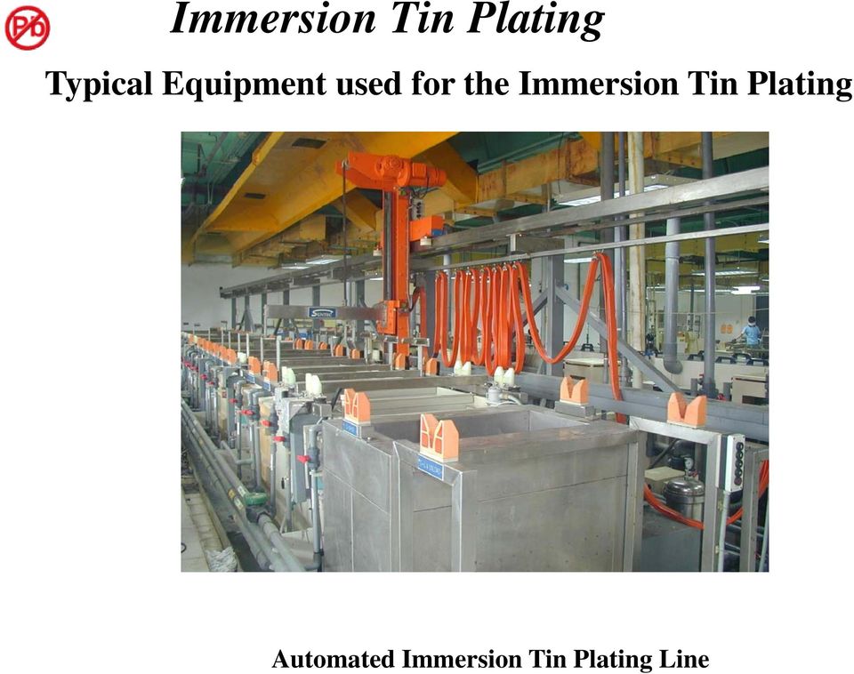
19 Immersion Tin Plating Typical Equipment used for the Immersion Tin Plating Automated Immersion Tin Plating Line
20 Immersion Sn (Immersion Tin) Typical Thickness: µm (25-60 µin) ADVANTAGES + Reliability Testing Results Comparable to ENIG + Good for Fine Pitch Product + Planar Surface + Cu/Sn Solderjoint + Inexpensive DISADVANTAGES - Panels Must be Routed and Tested Prior to Coating - Contains Thiourea, a Known Carcinogen - Limited Rework Cycles at CM - Horizontal Process Needs Nitrogen Blanket - Too Viscous for Small Holes; Backpanels Only - Handling Concerns

21 Immersion Palladium (Pd) Typical Thickness: 0.1 µm 10 µm (4-400 µin) ADVANTAGES DISADVANTAGES + Good Solderability - Availability + Cu/Sn Solderjoint - Possibly Issues with Solder Pot on Wave + Used in Automotive Sector - Handling Concerns
22 Electrolytic Plating Electrolytic plating is achieved by passing an electric current through h a solution containing i dissolved d metal ions. The PCB panel then serves as the cathode in an electrochemical cell, attracting the dissolved metal ions from the solution. The process includes controlling of plating parameters including voltage and amperage, temperature, time, and purity of bath solutions. Operators rack panels that carry the part from bath to bath (in a batch process).
23 Electrolytic Plating Electrolytic Nickel-Gold (Depicted Below) Nickel P C B Solution Nicke el Then Gold P C B Solution Titani ium Anode Cathode Anode Electrolytic Nickel Plating Anode Cathode Anode Electrolytic Gold Plating (Over Nickel)
24 Electrolytic Plating of Nickel an Gold Typical Equipment used for the Electrolytic Plating of Nickel and Gold Automated Nickel and Gold Plating Line g PAL and TAB Lines Shown
25 Electrolytic (Hard) Nickel / Gold Typical SMT Thickness: µm( µ in) Gold over µm ( µ in) Nickel ADVANTAGES + Plated Ni/Au Can be Used as an Etch Resist + Available for Mixed Technology Products + Au Wire-Bondable + Long Shelf Life DISADVANTAGES - Exposed Cu Sidewalls - Nickel Slivers Likely After S.E.S. S - Costly Process - Poor throwing Power Typical GF Thickness: µm (30-60 µ in) Hard Gold over µm ( µ in) Nickel
26 Selective Solder Plating Typical Equipment used for the Solder Plating Manual Tin-Lead Plating Line
27 Selective Solder Strip (SSS) Typical Thickness: 7 20 µm ( µ in) ADVANTAGES + Hot Bar Reflow for TAB Devices + Alternative to HASL on Thick Product DISADVANTAGES - Multiple Resist and Photo Cycles - Difficulty in Controlling Plated Sn/Pb Thickness - Overlap (Butt) Line Difficult to Control - Expensive - Contains Lead
28 Dip Coatings HASL (Hot Air Solder Level) OSP (Organic Solderability Preservative) Manifold PCB Coating Chemistry Sump OR C O A T I N G P C B C H E M I S T R Y Conveyorized Dip Module Vertical Dip Tank
29 OSP (Organic Solderability Preservative) Typical Equipment used for the Coating of OSP Conveyorized Horizontal OSP and Pre-Flux Line
30 OSP (Organic Solderability Preservative) (Entek 106A(X), Shikoku Glicote SMD-E2L, Tamura Solderite) Typical Thickness: µm (8-24 µ in) ADVANTAGES + Flat, Coplanar pads + Reworkable (at PCB Fabricator) + Doesn t Affect Finished Hole Size + Short, Easy Process + Low Cost + Benign to Soldermask + Cu/Sn Solderjoint DISADVANTAGES - Not a Drop-In Process (assy adjustments are required) - Difficult to Inspect - Questions Over Reliability of Exposed Copper After Assembly - Limited Thermal Cycles - Reworked at CM?; Sensitive to Some Solvents Used dfor Misprint i Cleaning - Limited Shelf life - Panels Need to be Routed and Tested Prior to Coating (ET Probe Issue) - Handling Concerns
31 High Temp OSP (Organic Solderability Preservative) (Entek 106A HT, Shikoku Glicote SMD-F1, Tamura WPF-21) Typical Thickness: µm (8-24 µ in) ADVANTAGES DISADVANTAGES + Flat, Coplanar pads + Reworkable (by Fabricator) + Short, Easy Process + Benign to Soldermask + Cu/Sn Solderjoint - Availability - Not a Drop-In Process (assy adjustments are required) - Difficult to Inspect - Questions Over Reliability of Exposed Copper After Assembly - Limited Thermal Cycles - Reworked at CM?; Sensitive to Some Solvents Used for Misprint Cleaning - Limited Shelf life - Panels Need to be Routed and Tested Prior to Coating (ET Probe Issue) - Copper Dissolution into Solder Volume - Handling Concerns
32 OSP and Selective ENIG ADVANTAGES + Advantages of OSP for SMT + Advantages of ENIG in through-holes + Cu/Sn Solderjoint + Can be used din Lead-Free DISADVANTAGES - Complex process for PCB suppliers - Larger Currently being used in today s handheld portable products (aka, Combi-Finish or SIT)
33 HASL (Hot Air Solder Level) Typical Equipment used for the Coating of HASL Vertical and Horizontal HASL Equipment
34 HASL (Hot Air Solder Level) LEADED Version Typical Thickness: µm ( µ in) ADVANTAGES + Nothing Solders Like Solder + Easily Applied + Lengthy Industry Experience + Easily Reworked + Multiple Thermal Excursions + Good Bond Strength + Long Shelf Life + Easy Visual Inspection + Cu/Sn Solderjoint DISADVANTAGES S - Co-Planarity Difference Potential Off-Contact Paste Printing - Inconsistent Coating Thicknesses (on Varying Pad Sizes) - Contains Lead - Not Suited for High Aspect Ratios - Not Suited for fine-pitch SMT and Grid Array Packages - PWB Dimensional Stability Issues - Bridging gproblems on Fine Pitch - Subjects the PCB to High Temp
35 HAL (Hot Air Level) UNLEADED Version Equipment being used for the Coating of Lead-Free HAL Same as for Leaded Versions but with a few Modifications Higher Temp Steel Solder Pots and Stronger - Higher Temp Pumps (Effective heat transfer by improved alloy circulation) Pre-heat panel (pre-dip) Longer contact t time with PCB High temperature resistant chemistries (oils and fluxes) Copper control (Drossing Dilution and Skimming) *Source: CEMCO / FSL
36 HASL (Hot Air Level) UNLEADED Version inemi Test Panels: Sn-0.3%Ag-0.7%Cu μm Sn-3%Ag-0.5%Cu μm Sn-0.7Cu + Ni μm ADVANTAGES DISADVANTAGES - Co-Planarity Difference + Easily Applied and Reworked Potential Off-Contact Paste Printing + Familiar HAL Dynamics - Inconsistent Coating Thicknesses + Good Bond Strength (on Varying Pad Sizes) + Long Shelf Life - Not Suited for High Aspect Ratios + Easy Visual Inspection - May not be suited for fine-pitch SMT (Wettability) and Grid Array Packages + Cu/Sn Solderjoint - PWB Dimensional Stability Issues - Bridging Problems on Fine Pitch - Subjects the PCB to VERY High Temp - Copper Feature Dissolution - Dull and Grainy Appearance - More Process Controls Req d
37 Lead-Free Solder Options ALLOY SYSTEM COMPOSITION MELTING RANGE ( o C) Sn-Ag Sn-3.5Ag 221 Sn-2Ag Sn-Cu Sn-0.7Cu 227 Sn-Ag-Bi Sn-3.5Ag-3Bi Sn-7.5Bi-2Ag Sn-Ag-Cu Sn-3.8Ag-0.7Cu ~217 Eutectic ti Sn-4Ag-0.5Cu 05C ~217 Sn-4.7Ag-1.7Cu ~217 SAC305 Sn-3.0Ag-0.5Cu ? SACX0307 Sn~0 0.9Cu~0.17Ag~0.14Bi Sn-Ag-Cu-Sb Sn-2Ag-0.8Cu-0.5Sb Sn-Zn-Bi Sn-7Zn-5Bi EUTECTIC ALLOYS *Source: Nihon Superior Co., LTD
38 Lead-Free Solder Process Parameters for Lead-Free HAL with Ni-Stabilized Sn-0.7Cu The main considerations in changing a HAL process from 63/37 Sn/Pb to SN100C (Ni-stabilized Sn-0.7Cu) is: The higher h melting point ALLOY MELTING POINT PROCESS TEMPERATURE PROCESS WINDOW 63/37 Sn/Pb 183 C 250 C(482) 67 C Sn-0.7Cu+Ni 227 C 265 C(509) 38 C *Source: Nihon Superior Co., LTD
39 Lead-free HAL running SN100C There are now about 80+ shops operating lead-free HAL machines in Europe. Running Lead free HAL machines in USA (Currently around 18 units) (~400 in the World) High Volume Production is determined by demand. So proportionately, the need for lead-free boards is still relatively small. Source: Florida CirTech, Inc. and Nihon Superior Co., LTD
40 Lead-free HASL in Europe Company Machine Supplier AT&S Pentagal Dünkel & Schürholz Quicksilver Ramaer Lantronic Vogt-Fuba / Dresden Quicksilver Brautmeier (Leiterplatten) Quicksilver Greule Quicksilver Piu-Printex Quicksilver Schwerdtfeger Pentagal Photochemie Quicksilver These companies have machines installed for lead-free HAL There are now 80+ operating HAL machines in Europe. (~400 in the World) Production volume is determined by demand for lead-free boards which is still small Source: Florida CirTech, Inc.
41 Running Lead free HAL machines in USA (Currently around 18 units) Pentaplex Elgin, IL Quicksilver American PCB Dallas, TX Lantronic Texas Circuitry Dallas, TX Lantronic Multilayer Dallas, TX Lantronic ElectroCircuits Toronto, Canada Lantronic Excell Electrocircuits Detroit, MI Lantronic Monitrol Elk Grove, IL Argus Calumet Electronics Calumet, MI Quicksilver Bartlett Mfg Cary, IL Argus Galaxy Circuits New Jersey Avalon Saturn Michigan Lantronic SMG Circuits New Jersey Argus Advance Electronics Colorado Penta Source: Florida CirTech, Inc.
42 HAL (Hot Air Level) UNLEADED Version Equipment Trials / Findings using Lead-Free HAL Alloy Melting point Process temperature Sn/Pb 183º C 250º C HAL Lead-free 217 to 227º C 265 to 280º C Stainless Steel Erosion Source: Florida CirTech, Inc.
43 LEAD-FREE HAL (Hot Air Level) EROSION OF COPPER PAD Oi Original i lpad 18μm Copper After 6 Passes over Wave Soldering Machine 105 C Preheat, 256 C Solder Temperature, 4 seconds contact time Sn-37Pb Sn-3.0Ag-0.5Cu Sn-0.7Cu+Ni Source: Florida CirTech, Inc.
44 LEAD-FREE HAL (Hot Air Level) Dissolution rate of Copper Copper Dissolution Rates of various Lead-Free Alloys. Source: Circuits Assembly OCTOBER 2004
45 Lead free Assembly Equipment in the World SN100C - >1800 Wave Soldering units >200 in Europe 100 in the USA The key point in running lead-free processes is acknowledging that the process window is smaller than for tin-lead solder Source: Florida CirTech, Inc.
Solutions without Boundaries. PCB Surface Finishes. Todd Henninger, C.I.D. Sr. Field Applications Engineer Midwest Region
 Solutions without Boundaries PCB Surface Finishes Todd Henninger, C.I.D. Sr. Field Applications Engineer Midwest Region 1 Notice Notification of Proprietary Information: This document contains proprietary
PRINTED CIRCUIT BOARD SURFACE FINISHES - ADVANTAGES AND DISADVANTAGES
 PRINTED CIRCUIT BOARD SURFACE FINISHES - ADVANTAGES AND DISADVANTAGES By Al Wright, PCB Field Applications Engineer Epec Engineered Technologies Anyone involved within the printed circuit board (PCB) industry
SURFACE FINISHES. Technical Webinar DELIVERING QUALITY SINCE 1952.
 SURFACE FINISHES Technical Webinar DELIVERING QUALITY SINCE 1952. Overview: The printed circuit board surface finish forms a critical interface between the component to be assembled and the bare PCB. The
PRODUCT PROFILE. ELECTROLOY in partnership with FCT Asia Pte Limited. in manufacturing. Nihon Superior Lead Free Solder Bar.
 PRODUCT PROFILE ELECTROLOY in partnership with FCT Asia Pte Limited in manufacturing Nihon Superior Lead Free Solder Bar SN100C Product Name Product Code LEAD FREE BAR LEAD FREE BAR ( TOP UP ALLOY ) SN100C
Lead Free Wave Soldering
 China - Korea - Singapore- Malaysia - USA - Netherlands - Germany WAVE SELECTIVE REFLOW SOLDERING SOLDERING SOLDERING Lead Free Wave Soldering Ursula Marquez October 18, 23 Wave Soldering Roadmap Parameter
Lead-free Wave Soldering Some Insight on How to Develop a Process that Works
 Lead-free Wave Soldering Some Insight on How to Develop a Process that Works Author: Peter Biocca, Senior Market Development Engineer, Kester, Des Plaines, Illinois. Telephone: 972.390.1197; email [email protected]
How to Build a Printed Circuit Board. Advanced Circuits Inc 2004
 How to Build a Printed Circuit Board 1 This presentation is a work in progress. As methods and processes change it will be updated accordingly. It is intended only as an introduction to the production
Printed Circuit Design Tutorial
 Printed Circuit Design Tutorial By Gold Phoenix Technology Tech Center, [email protected] Gold Phoenix has been sale PCB board in North America since 2003, during these years we received a lot of
CHAPTER 5. OVERVIEW OF THE MANUFACTURING PROCESS
 CHAPTER 5. OVERVIEW OF THE MANUFACTURING PROCESS 5.1 INTRODUCTION The manufacturing plant considered for analysis, manufactures Printed Circuit Boards (PCB), also called Printed Wiring Boards (PWB), using
SURFACE FINISHING FOR PRINTED CIRCUIT BOARDS
 SURFACE FINISHING FOR PRINTED CIRCUIT BOARDS In a world of ever-increasing electronic component complexity and pin count requirements for component packaging, focus is once again on the age-old question
Effect of PWB Plating on the Microstructure and Reliability of SnAgCu Solder Joints
 Effect of PWB Plating on the Microstructure and Reliability of SnAgCu Solder Joints Y. Zheng, C. Hillman, P. McCluskey CALCE Electronic Products and Systems Center A. James Clark School of Engineering
Technical Note Recommended Soldering Parameters
 Technical Note Recommended Soldering Parameters Introduction Introduction The semiconductor industry is moving toward the elimination of Pb from packages in accordance with new international regulations.
Specification for Electroless Nickel/ Electroless Palladium/ Immersion Gold (ENEPIG) Plating for Printed Circuit Boards
 Plating for Printed Circuit Boards") Specification for Electroless Nickel/ Electroless Palladium/ Immersion Gold (ENEPIG) Plating for Printed Circuit Boards Developed by the Plating Processes Subcommittee (4-14) of the Fabrication Processes
Specification for Electroless Nickel/ Electroless Palladium/ Immersion Gold (ENEPIG) Plating for Printed Circuit Boards Developed by the Plating Processes Subcommittee (4-14) of the Fabrication Processes
How do you create a RoHS Compliancy-Lead-free Roadmap?
 How do you create a RoHS Compliancy-Lead-free Roadmap? When a company begins the transition to lead-free it impacts the whole organization. The cost of transition will vary and depends on the number of
CONSIDERATIONS FOR SELECTING A PRINTED CIRCUIT BOARD SURFACE FINISH
 CONSIDERATIONS FOR SELECTING A PRINTED CIRCUIT BOARD SURFACE FINISH Randy Schueller, Ph.D. DfR Solutions Minneapolis, MN, USA [email protected] ABSTRACT The selection of the surface finish to
Dissimilar Metal Corrosion
 PDHonline Course S118 (1 PDH) Dissimilar Metal Corrosion Instructor: D. Matthew Stuart, P.E., S.E., F.ASCE, F.SEI, SECB, MgtEng 2013 PDH Online PDH Center 5272 Meadow Estates Drive Fairfax, VA 22030-6658
Printed Circuits. Danilo Manstretta. microlab.unipv.it/ [email protected]. AA 2012/2013 Lezioni di Tecnologie e Materiali per l Elettronica
 Lezioni di Tecnologie e Materiali per l Elettronica Printed Circuits Danilo Manstretta microlab.unipv.it/ [email protected] Printed Circuits Printed Circuits Materials Technological steps Production
How to manage wave solder alloy contaminations. Gerjan Diepstraten & Harry Trip Cobar Europe BV Balver Zinn
 How to manage wave solder alloy contaminations Gerjan Diepstraten & Harry Trip Cobar Europe BV Balver Zinn Content SnPb solder and impurities Lead-free solder change Pb contaminations in lead-free Measure
Customer Service Note Lead Frame Package User Guidelines
 Customer Service Note Lead Frame Package User Guidelines CSN30: Lead Frame Package User Guidelines Introduction Introduction When size constraints allow, the larger-pitched lead-frame-based package design
DRIVING COST OUT OF YOUR DESIGNS THROUGH YOUR PCB FABRICATOR S EYES!
 4/3/2013 S THROUGH YOUR PCB FABRICATOR S EYES! Brett McCoy Eagle Electronics Schaumburg IL. New England Design and Manufacturing Tech Conference Brett McCoy: Vice President / Director of Sales Circuit
Good Boards = Results
 Section 2: Printed Circuit Board Fabrication & Solderability Good Boards = Results Board fabrication is one aspect of the electronics production industry that SMT assembly engineers often know little about.
Electroless Nickel / Immersion Gold Process Technology for Improved Ductility of Flex and Rigid-Flex Applications
 M44.44kk-growth Electroless Nickel / Immersion Gold Process Technology for Improved Ductility of Flex and Rigid-Flex Applications By: Kuldip Johal and Hugh Roberts - Atotech USA Inc. Sven Lamprecht and
ENIG with Ductile Electroless Nickel for Flex Circuit Applications
 ENIG with Ductile Electroless Nickel for Flex Circuit Applications Yukinori Oda, Tsuyoshi Maeda, Chika Kawai, Masayuki Kiso, Shigeo Hashimoto C.Uyemura & Co., Ltd. George Milad and Donald Gudeczauskas
Analysis of BGA Solder Joint Reliability for Selected Solder Alloy and Surface Finish Configurations
 Analysis of BGA Solder Joint Reliability for Selected Solder Alloy and Surface Finish Configurations Hugh Roberts / Atotech USA Inc Sven Lamprecht and Christian Sebald / Atotech Deutschland GmbH Mark Bachman,
The Study, Measurement, and Prevention of Tarnish on Immersion Silver Board Finishes
 The Study, Measurement, and Prevention of Tarnish on Immersion Silver Board Finishes Lenora Toscano and Donald Cullen MacDermid, Inc. Waterbury, CT USA ABSTRACT With increased environmental legislation
Review of the Impact of Intermetallic Layers on the Brittleness of Tin-Lead and Lead-Free Solder Joints
 Review of the Impact of Intermetallic Layers on the Brittleness of Tin-Lead and Lead-Free Solder Joints Per-Erik Tegehall, Ph.D. 6-03-15 Preface This review has been funded by Vinnova (Swedish Governmental
Rogers 3003, 3006, 3010, 3035, 3203, 3206, 3210
 Stocked Materials: RIGID STANDARD FR4 High Tg 170c Black FR4 Polyclad 370HR (Lead Free) HIGH RELIABILITY Polyimide (Arlon 85N, Isola P96) BT (G200) HIGH FREQUENCY: Park Nelco 4000-13, 4000-13si Getek Gore
Thermal Management Solutions for Printed Circuit Boards used in Digital and RF Power Electronics and LED assemblies
 Thermal Management Solutions for Printed Circuit Boards used in Digital and RF Power Electronics and LED assemblies Sandy Kumar, Ph.D. Director of Technology American Standard Circuits, Inc 3615 Wolf Road
Soldering of EconoPACK TM, EconoPIM TM, EconoBRIDGE TM, EconoPACK +, EconoDUAL, EasyPACK and EasyPIM TM - Modules
 Seite 1 Soldering of EconoPACK TM, EconoPIM TM, EconoBRIDGE TM, EconoPACK +, EconoDUAL, EasyPACK and EasyPIM TM - Modules Soldering with alloys containing lead (SnPb) is the standard connection technology
Selective Soldering Defects and How to Prevent Them
 Selective Soldering Defects and How to Prevent Them Gerjan Diepstraten Vitronics Soltec BV Introduction Two major issues affecting the soldering process today are the conversion to lead-free soldering
COPPER FLEX PRODUCTS
 COPPER FLEX PRODUCTS WHY FLEX? Molex ible Printed Circuit Technology is the answer to your most challenging interconnect applications. We are your total solution for ible Printed Circuitry because we design
Anodes and Misc Equipment
 Anodes and Misc Equipment Application: Platinised Titanium Anodes Platinised titanium anodes are recommended for use in the following electrolytic processes:- Precious metal electroplating - e.g. Au, Pt,
Neutral type Auto-Catalytic Electroless Gold Plating Process Abstract 1. Introduction 2. Experiment and Results
 Neutral type Auto-Catalytic Electroless Gold Plating Process Don Gudeczauskas, Uyemura International Corporation Seiji Nakatani, Masayuki Kiso, Shigeo Hashimoto, C.Uyemura & Co., Ltd Abstract In order
Safety Certification for Lead Free Flexible and Rigid-Flex PCBs
 Safety Certification for Lead Free Flexible and Rigid-Flex PCBs Crystal Vanderpan Underwriters Laboratories Inc. March 27, 2007 Crystal Vanderpan Principal Engineer for Printed Circuit Technologies Joined
FABRICATION 2011 SERVICES TECHNOLOGIES CAPABILITIES INDUSTRY
 FABRICATION 2011 SERVICES 24HRS - 5 DAYS ON QUICK TURN PROTOTYPE Dear Customer, We would like to take this opportunity to welcome you and thank you for looking to ASA PCB as your Printed Circuit Manufacturing
Q&A. Contract Manufacturing Q&A. Q&A for those involved in Contract Manufacturing using Nelco Electronic Materials
 Q&A Q&A for those involved in Contract Manufacturing using Nelco Electronic Materials 1. Do Nelco laminates have any discoloration effects or staining issues after multiple high temperature exposures?
Alternatives To HASL: Users Guide For Surface Finishes
 Alternatives To HASL: Users Guide For Surface Finishes By Dan T. Parquet and David W. Boggs Merix Corporation, Forest Grove, OR INTRODUCTION A great deal of controversy continues to surround the use of
Auditing a Printed Circuit Board Fabrication Facility Greg Caswell
 Auditing a Printed Circuit Board Fabrication Facility Greg Caswell Introduction DfR is often requested to audit the PCB fabrication process of a customer s supplier. Understanding the process variations
17 IMPLEMENTATION OF LEAD-FREE SOLDERING TECHNOLOGY. Eva Kotrčová České Vysoké Učení Technické Fakulta Elektrotechnická Katedra Elektrotechnologie
 17 IMPLEMENTATION OF LEAD-FREE SOLDERING TECHNOLOGY Eva Kotrčová České Vysoké Učení Technické Fakulta Elektrotechnická Katedra Elektrotechnologie 1. Introduction Lead is the toxic heavy metal which is
Dynamic & Proto Circuits Inc. Corporate Presentation
 Dynamic & Proto Circuits Inc. Corporate Presentation 1 DAPC Facility 54,000 Sq.ft./6,000 Sq.M 2 Multilayer Process 3 Solder Mask Options BLUE BLACK RED GREEN DRY FILM CLEAR 4 Investing in Technology New
Lead-Free Rework Optimization Project
 Lead-Free Rework Optimization Project Project Co-Chairs: Jasbir Bath, Flextronics International Craig Hamilton, Celestica IPC APEX 2008 Background Reliability tests in the previous inemi lead-free assembly
Introduction to the Plastic Ball Grid Array (PBGA)
") Introduction to the Plastic Ball Grid Array (PBGA) Q1, 2008 Terry Burnette Dec. 15, 2005 Presentation Outline PBGA Introduction and Package Description PC Board Design for PBGA PBGA Assembly PBGA Solder
Introduction to the Plastic Ball Grid Array (PBGA) Q1, 2008 Terry Burnette Dec. 15, 2005 Presentation Outline PBGA Introduction and Package Description PC Board Design for PBGA PBGA Assembly PBGA Solder
Historical production of rigid PCB s
 Historical production of rigid PCB s The Printed Circuit Board (PCB) The PCB What is a Printed Circuit Board? Green plastic thing with holes!! (green plastic syndrome) Platform for components Image with
Wetting Behavior of Pb-free Solder on Immersion Tin Surface Finishes in Different Reflow Atmospheres
 Wetting Behavior of Pb-free Solder on Immersion Tin Surface Finishes in Different Reflow Atmospheres Sven Lamprecht 1, Dr. Kenneth Lee 2, Bill Kao 3, Günter Heinz 1 1 Atotech Deutschland GmbH, Berlin,
Flexible Circuit Simple Design Guide
 Flexible Circuit Simple Design Guide INDEX Flexible Circuit Board Types and Definitions Design Guides and Rules Process Flow Raw Material Single Side Flexible PCB Single Side Flexible PCB (Cover layer
Flex Circuit Design and Manufacture.
 Flex Circuit Design and Manufacture. Hawarden Industrial Park, Manor Lane, Deeside, Flintshire, CH5 3QZ Tel 01244 520510 Fax 01244 520721 [email protected] www.merlincircuit.co.uk Flex Circuit
AND8464/D. Board Level Application Note for 0402, 0502 and 0603 DSN2 Packages APPLICATION NOTE
 Board Level Application Note for 0402, 0502 and 0603 DSN2 Packages Prepared by: Denise Thienpont, Steve St. Germain ON Semiconductor APPLICATION NOTE Introduction ON Semiconductor has introduced an expanded
Choosing a Low-Cost Alternative to SAC Alloys for PCB Assembly
 Choosing a Low-Cost Alternative to SAC Alloys for PCB Assembly Our thanks to Indium Corporation for allowing us to reprint the following article. By Brook Sandy and Ronald C. Lasky, PhD, PE., Indium Corporation
Bob Willis leadfreesoldering.com
 Assembly of Flexible Circuits with Lead-Free Solder Alloy Bob Willis leadfreesoldering.com Introduction to Lead-Free Assembly Video Clips Component www.bobwillis.co.uk/lead/videos/components.rm Printed
Mounting of Meritec SMT Products Using Lead-Free Solder
 Mounting of Meritec SMT Products Using Lead-Free Solder 10/10/08 rev B Mounting of Meritec SMT Products Using Lead-Free Solder Contents Page 2 Scope Page 3 Test Samples/Preparation Page 3 Facilities/Equipment
Comparative Wetting Ability of Lead-Free Alloys
 Comparative Wetting Ability of Lead-Free Alloys Understanding the wetting kinetics of lead-free alloys becomes crucial in selecting a suitable lead-free composition for assembling PCBs. KaiHwa Chew, Vincent
Aspocomp, PCBs for Demanding Applications
 HDI PIIRILEVYT Aspocomp, PCBs for Demanding Applications Automotive Electronics Industrial Electronics Mobile Devices Base Station Photos ABB, Aspocomp, Vacon and Wabco PCBs for Base Stations and Other
Introduction to Photolithography Concepts via printed circuit board (PCB) manufacturing. PCB Background Information (courtesy of Wikipedia)
 manufacturing. PCB Background Information (courtesy of Wikipedia)") Introduction to Photolithography Concepts via printed circuit board (PCB) manufacturing Introduction As you saw on the video (http://www.youtube.com/watch?v=9x3lh1zfggm), photolithography is a way to nanomanufacture
Introduction to Photolithography Concepts via printed circuit board (PCB) manufacturing Introduction As you saw on the video (http://www.youtube.com/watch?v=9x3lh1zfggm), photolithography is a way to nanomanufacture
PCB Assembly Guidelines for Intersil Wafer Level Chip Scale Package Devices
 Assembly Guidelines for Intersil Wafer Level Chip Scale Package Devices Introduction There is an industry-wide trend towards using the smallest package possible for a given pin count. This is driven primarily
Chapter 13: Electrochemistry. Electrochemistry. The study of the interchange of chemical and electrical energy.
 Chapter 13: Electrochemistry Redox Reactions Galvanic Cells Cell Potentials Cell Potentials and Equilbrium Batteries Electrolysis Electrolysis and Stoichiometry Corrosion Prevention Electrochemistry The
, Yong-Min Kwon 1 ) , Ho-Young Son 1 ) , Jeong-Tak Moon 2 ) Byung-Wook Jeong 2 ) , Kyung-In Kang 2 )
 , Ho-Young Son 1 ) , Jeong-Tak Moon 2 ) Byung-Wook Jeong 2 ) , Kyung-In Kang 2 )") Effect of Sb Addition in Sn-Ag-Cu Solder Balls on the Drop Test Reliability of BGA Packages with Electroless Nickel Immersion Gold (ENIG) Surface Finish Yong-Sung Park 1 ), Yong-Min Kwon 1 ), Ho-Young
Effect of Sb Addition in Sn-Ag-Cu Solder Balls on the Drop Test Reliability of BGA Packages with Electroless Nickel Immersion Gold (ENIG) Surface Finish Yong-Sung Park 1 ), Yong-Min Kwon 1 ), Ho-Young
Printed Circuit Board - PCB presentation
 Printed Circuit Board - PCB presentation PCB application P&A supplies customer with Quick Turn Prototype, Small and Medium-volume PCBs. The PCBs can be widely used in communication product, eg. Bluetooth,
PC/104, PC/104 -Plus, VarPol connectors
 164 PC/104, PC/104 -Plus, VarPol connectors Definitions 166 Technical specifications 168 Hole specifications 169 PC/104 170 PC/104-Plus 172 Accessories: PC/104 and PC/104-Plus 174 VarPol angled pin header
Product Specification
 Product Specification Model No.: DC-240-L01-00-TR Description: H=3.00mm Horizontal SMD DC Power Jacks Pin Shaft Diameter: 0.65mm Packing Method: Tape & Reel (600pcs./R) 1. General 1a. Scope The jacks should
Electronic Board Assembly
 Electronic Board Assembly ERNI Systems Technology Systems Solutions - a one stop shop - www.erni.com Contents ERNI Systems Technology Soldering Technologies SMT soldering THR soldering THT soldering -
How to avoid Layout and Assembly got chas with advanced packages
 How to avoid Layout and Assembly got chas with advanced packages Parts and pitch get smaller. Pin counts get larger. Design cycles get shorter. BGA, MicroBGA, QFN, DQFN, CSP packages are taking the design
An Ammonium-free, Acid. Zinc/Nickel (12-15% Ni) Process
 Process") An Ammonium-free, Acid Zinc/Nickel (12-15% Ni) Process Requirements of an acid zinc/nickel process Technical requirements High plating speed (current efficiency up to 90 %) High thicknesses of deposits
An Ammonium-free, Acid Zinc/Nickel (12-15% Ni) Process Requirements of an acid zinc/nickel process Technical requirements High plating speed (current efficiency up to 90 %) High thicknesses of deposits
REVISION HISTORY APPROVERS
 REVISION HISTORY Revision Description of Change Writer/Reviser Effective Date 1.0 As Issued. Renumbered from PEC-MAT-2-003-00. Lenora Bennett January 23, 2012 2.0 Updated Table 1 Nickel barrier specifications
Printed Circuit Board Quick-turn Prototyping and Production
 Printed Circuit Board Quick-turn Prototyping and Production Who We Are Bay Area Circuits has been serving the Printed Circuit Board (PCB) manufacturing needs of high-tech electronics manufacturers, contract
Electroplating with Photoresist Masks
 Electroplating with Photoresist Masks Revised: 2014-01-17 Source: www.microchemicals.com/downloads/application_notes.html Electroplating - Basic Requirements on the Photoresist Electroplating with photoresist
Lead-Free Soldering and Environmental Compliance: An Overview
 CHAPTER 1 Lead-Free Soldering and Environmental Compliance: An Overview Dongkai Shangguan, Flextronics International Introduction Solder interconnects perform three major functions: electrical, mechanical,
Advanced Technologies and Equipment for 3D-Packaging
 Advanced Technologies and Equipment for 3D-Packaging Thomas Oppert Semicon Russia 15 th May 2014 Outline Short Company Introduction Electroless Plating on Wafer Level Ultra-SB 2 - Wafer Level Solder Balling
Lead-free Hand-soldering Ending the Nightmares
 Lead-free Hand-soldering Ending the Nightmares Most issues during the transition seem to be with Hand-soldering As companies transition over to lead-free assembly a certain amount of hand-soldering will
PCB RoHS Update OCT08 ELECTRONICS MANUFACTURING SERVICES
 PCB RoHS Update CT08 ELECTRNICS MANUFACTURING SERVICES 2006 Sanmina-SCI Corporation. Sanmina-SCI is a trademark of Sanmina-SCI Corporation. All trademarks and registered trademarks are the property of
The Move to Lead-Free Solders
 Why Lead-free? The Move to Lead-Free Solders Introduction A very important issue which will ultimately concern manufacturing operations throughout the World is the pending conversion to Lead-free solders.
LEAD FREE HALOGENFREE. Würth Elektronik PCB Design Conference 2007. Lothar Weitzel 2007 Seite 1
 LEAD FREE HALOGENFREE Würth Elektronik PCB Design Conference 2007 Lothar Weitzel 2007 Seite 1 Content Solder surfaces/overview Lead free soldering process requirements/material parameters Different base
Count on Optima Technology Associates to meet your requirements
 Since 1995, Global Resources, Local Support When you need quality Printed Circuit Boards To Spec On Time On Budget Count on Optima Technology Associates to meet your requirements Optima Technology Associates,
Lead & Magnet Wire Connection Methods Using the Tin Fusing Method Joyal A Division of AWE, Inc.
 Lead & Magnet Wire Connection Methods Using the Tin Fusing Method Joyal A Division of AWE, Inc. Abstract The technology for connecting lead and magnet wires for electric motors and electro mechanical devices
Compliant Terminal Technology Summary Test Report
 Engineering Report ER04100 October 5th, 2004 Revision A Copyright Autosplice Inc., September 2004 Table of Contents Summary Overview 3 Compliant Terminal Specifications 3 Test Plan 4 Test Conditions 4
First Published in the ECWC 10 Conference at IPC Printed Circuits Expo, Apex and Designer Summit 2005, Anaheim, Calif., Feb.
 First Published in the ECWC 10 Conference at IPC Printed Circuits Expo, Apex and Designer Summit 2005, Anaheim, Calif., Feb. 22-24, 2005 Test and Inspection as part of the lead-free manufacturing process
UNIT 4 METAL COATING PROCESSES
 UNIT 4 METAL COATING PROCESSES Structure 4.1 Introduction Objectives 4.2 Metal and Non-metal Coatings 4.2.1 Metallic Coatings 4.2.2 Non-Metallic Coatings 4.3 Electroforming 4.4 Galvanizing 4.5 Anodizing
FEATURES AND BENEFITS OF DIFFERENT PLATINUM ALLOYS. Kris Vaithinathan and Richard Lanam Engelhard Corporation
 FEATURES AND BENEFITS OF DIFFERENT PLATINUM ALLOYS Kris Vaithinathan and Richard Lanam Engelhard Corporation Introduction There has been a significant increase in the world wide use of platinum for jewelry
ALPHA CVP-390 - NO-CLEAN, LEAD-FREE SOLDER PASTE ZERO-HALOGEN, LOW VOIDS, FINE FEATURE, EXCELLENT PIN TEST PERFORMANCE, SAC305 AND LOW AG CAPABLE.
 T E C H N I C A L B U L L E T I N ALPHA CVP-390 - NO-CLEAN, LEAD-FREE SOLDER PASTE ZERO-HALOGEN, LOW VOIDS, FINE FEATURE, EXCELLENT PIN TEST PERFORMANCE, SAC305 AND LOW AG CAPABLE. DESCRIPTION ALPHA CVP-390
Best Practices for Improving the PCB Supply Chain: Performing the Process Audit
 Best Practices for Improving the PCB Supply Chain: Performing the Process Audit Cheryl Tulkoff, Greg Caswell, Dr. Craig Hillman DfR Solutions Beltsville, MD USA [email protected], [email protected],
FLEXIBLE CIRCUITS MANUFACTURING
 IPC-DVD-37 FLEXIBLE CIRCUITS MANUFACTURING Below is a copy of the narration for DVD-37. The contents of this script were developed by a review group of industry experts and were based on the best available
Atomic Structure. Atoms consist of: Nucleus: Electrons Atom is electrically balanced equal electrons and protons. Protons Neutrons
 Basics of Corrosion Performance Metals Sacrificial anode manufacturer Specialize in aluminum alloy anodes All products made in the USA (Berks county, PA) ISO9001/2001 Certified Quality System Also traditional
3835 West Conflans, Irving, Texas 75061 [email protected] Call Us at (972) 790-0062 Fax (972) 790-0293
 790-0062 Fax (972) 790-0293") Multilayer Technology An AS9100 & ISO 9001:2008 Company Multilayer Technology is a full service PCB provider specializing in high quality, high density, quick turn fabrication for time-critical solutions.
Multilayer Technology An AS9100 & ISO 9001:2008 Company Multilayer Technology is a full service PCB provider specializing in high quality, high density, quick turn fabrication for time-critical solutions.
Wurth Electronics Midcom Policy Statement on RoHS Compliance And Lead-Free Products
 Wurth Electronics Midcom Policy Statement on RoHS Compliance And Lead-Free Products General Environmental Policy Wurth Electronics Midcom is committed to the manufacture of environmentally-friendly products
PCB Board Design. PCB boards. What is a PCB board
 PCB Board Design Babak Kia Adjunct Professor Boston University College of Engineering Email: bkia -at- bu.edu ENG SC757 - Advanced Microprocessor Design PCB boards What is a PCB board Printed Circuit Boards
EXPERIMENT #9 CORROSION OF METALS
 EXPERIMENT #9 CORROSION OF METALS Objective The objective of this experiment is to measure the corrosion rate of two different metals and to show the effectiveness of the use of inhibitors to protect metals
Rework stations: Meeting the challenges of lead-free solders
 Rework stations: Meeting the challenges of lead-free solders Market forces, particularly legislation against the use of lead in electronics, have driven electronics manufacturers towards lead-free solders
Lead-free Defects in Reflow Soldering
 Lead-free Defects in Reflow Soldering Author: Peter Biocca, Senior Development Engineer, Kester, Des Plaines, Illinois. Telephone 972.390.1197; email [email protected] February 15 th, 2005 Lead-free Defects
3 Embedded Capacitor Material
 3 Embedded Capacitor Material Design and Processing Guidelines for Printed Circuit Board Fabricators Effective date: March 2004 Contents Overview Material Handling Process Compatibility Standard vs. Sequential
RoHS-Compliant Through-Hole VI Chip Soldering Recommendations
 APPLICATION NOTE AN:017 RoHS-Compliant Through-Hole VI Chip Soldering Recommendations Ankur Patel Associate Product Line Engineer Contents Page Introduction 1 Wave Soldering 1 Hand Soldering 4 Pin/Lead
Lead-Free Wave Soldering of High Complexity PWB s
 Lead-Free Wave Soldering of High Complexity PWB s The transition to lead-free wave soldering has brought with it many challenges. As with any new manufacturing technology entering a production environment,
Use of Carbon Nanoparticles for the Flexible Circuits Industry
 Use of Carbon Nanoparticles for the Flexible Circuits Industry Ying (Judy) Ding, Rich Retallick MacDermid, Inc. Waterbury, Connecticut Abstract FPC (Flexible Printed Circuit) has been growing tremendously
Amphenol Sincere. Electronic Integration & Flexible Printed Circuits. Aerospace. Health Care. Heavy Equipment HEV. Industrial
 Amphenol Sincere Health Care Aerospace Heavy Equipment HEV Industrial Electronic Integration & Flexible Printed Circuits About Amphenol The second largest manufacturers of interconnect products 87 worldwide
Difference Between Various Sn/Ag/Cu Solder Compositions. Almit Ltd. Tadashi Sawamura Takeo Igarashi
 Difference Between Various Sn/Ag/Cu Solder Compositions Almit Ltd. Tadashi Sawamura Takeo Igarashi 29/6/2005 Table Of Contents 1. Overview 2. Mechanical Properties 3. Reliability Results 4. Conclusion
How to Avoid Conductive Anodic Filaments (CAF)
") How to Avoid Conductive Anodic Filaments (CAF) Ling Zou & Chris Hunt 22 January 20 1 Your Delegate Webinar Control Panel Open and close your panel Full screen view Raise hand for Q&A at the end Submit
How to Avoid Conductive Anodic Filaments (CAF) Ling Zou & Chris Hunt 22 January 20 1 Your Delegate Webinar Control Panel Open and close your panel Full screen view Raise hand for Q&A at the end Submit
TAIYO PSR-4000 AUS703
 TAIYO PSR-4000 AUS703 LIQUID PHOTOIMAGEABLE SOLDER MASK Designed for Flip Chip Packaging Applications Halogen-Free (300ppm) Excellent Thermal and Crack Resistance Low Water Absorption RoHS Compliant Excellent
Objectives/Introduction Extraction of zinc Physical properties of zinc Zinc casting alloys Wrought zinc alloys Engineering design with zinc alloys
 Lecture 7 Zinc and its alloys Subjects of interest Objectives/Introduction Extraction of zinc Physical properties of zinc Zinc casting alloys Wrought zinc alloys Engineering design with zinc alloys Objectives
ALPHA OL-107F-A ZERO-HALOGEN, LOW VOIDS, FINE FEATURE, EXCELLENT PIN TEST PERFORMANCE, NO-CLEAN, LEAD-FREE SOLDER PASTE
 T E C H N I C A L B U L L E T I N ALPHA OL-107F-A ZERO-HALOGEN, LOW VOIDS, FINE FEATURE, EXCELLENT PIN TEST PERFORMANCE, NO-CLEAN, LEAD-FREE SOLDER PASTE DESCRIPTION ALPHA OL-107F-A is a lead-free, Zero-halogen
PRINTED CIRCUIT BOARD DESIGN AND MANUFACTURING CORP.
 PRINTED CIRCUIT BOARD DESIGN AND MANUFACTURING CORP. Corporate Information Established in 2004 Headquarter office in San Jose, CA Production factory located in Binh Duong, Vietnam - Center of hi-tech industrial
Metals and Non-metals. Comparison of physical properties of metals and non metals
 Metals and Non-metals Comparison of physical properties of metals and non metals PHYSICAL PROPERTY METALS NON-METALS Physical State Metallic lustre (having a shining surface) Mostly solids (Liquid -mercury)