OLED display. Ying Cao
|
|
|
- Norman Underwood
- 9 years ago
- Views:
Transcription
1 OLED display Ying Cao

2 Outline OLED basics OLED display A novel method of fabrication of flexible OLED display

3 Potentials of OLED Suitable for thin, lightweight, printable displays Broad color range Good contrast High resolution(<5 μm pixel size) Fast switching (1-10 μs) Wide viewing angle Low cost of materials
 Wide viewing angle Low cost of materials")
4 Energy level diagram of OLED Electrons injected from the cathode (Ca, Al, Ba, etc.) Holes injected from the anode (Indium/tin oxide, PANi, PEDOT) Transport and radiative recombination of electron hole pairs at the emissive polymer
 Transport and radiative recombination of electron")
5 A threshold voltage must be achieved to overcome the barriers to inject charges into the organic materials N 2 molecules doped during the evaporation of Alq 3 cause the expansion of the traps states below the LUMO thus lowering the injection barrier for electrons The J-V curves of bi-layer OLEDs with Alq 3 evaporated under different N 2 ambient pressure. The insert presents schematic structure diagram of OLEDs. [2]

6 OLED types Small-molecular OLED Made by vacuum evaporating small molecules to the substrate similar to that used in semiconductor manufacturing Well proven on fabrication of up to about 15 inches in diameter (shadow mask) Crystallization due to low glass transition temperature shortens lifetime and reliability Polymer OLED Made by depositing the polymer materials on substrates through an inkjet printing process or other solution processing methods under ambient conditions Fabrication of large screen sizes Oxidation of carbon-carbon bonds between the aromatic rings reduce the conjugation length of the polymer

7 Inkjet printing Ref. 3 Advantage: high-resolution, low cost, materials saving selectively deposit many layers in a display simultaneously Surface properties of the substrate affect the uniformity of the film thickness Problems: layer shift and dimentional changes from the PLED drying and evaporation process

8 OLED display First active-matrix full-color display by Sanyo in 1999

9 Challenges and shortcomings I Addressing schemes Huge driving currents are needed to achieve adequate average brightness in Passive Matrix addressing displays. Such large currents cause problems such as large drive voltages leading to increased power dissipation, excess flicker, and shortened lifetimes. Active Matrix addressing can be used to overcome such problems

10 Challenges and shortcomings II Brightness and Lifetime Requirements State of art OLED brightness and lifetime: 100 nits and 40,000 hours (50% initial luminance) High brightness level require the display driving voltage levels to be increased which trades off expected lifetime. For most OLED materials, the relationship between driving voltage level and lifetime is nearly linear. Moisture sensitivity Over time, moisture can react with the organic layers and cause degradation and defects in an OLED display Sealing techniques Inserting desiccants

11 Applications Current main commercial applications Mobile phone screen (Samsung/NEC, Motorola, LG) Car radio Digital camera (Kodak) Car stereo (Pioneer, TDK, Kenwood) Razor (Philips) Future Flexible displays Replacing incandescent and fluorescent light bulbs Currently power efficiency equivalent to incandescent light bulb while a factor of five less than that of fluorescent lighting

12 Flexible display Flexible substrate requirements Transparent Robustness Low cost Stability Low coefficient of thermal expansion Low moisture absorption Resistant to chemicals & solvents Processing temperatures limited by : Deformation temperature of material layers For common plastic materials, <300 ºC

13 Top-gate TFT process flow [4] 4-inch PET (Polyester), PEN (Polyethylenenapthalate) substrates Poly-Si formation by pulsed laser crystallization Low temperature (<100 ºC) gate oxide (~100 nm) formation Dopant activation by pulsed laser annealing the dopant layer
 formation Dopant activation by pulsed laser annealing the")
14 Pulsed Laser Crystallization (PLC) PLC converts a-si film (90 nm) to poly-si via ultrafast melting and solidification. SiO 2 buffer layer prevent the heat to be transferred to the substrate Plastic kept below 250 ºC, cools rapidly

15 TFT results [4] NMOS PMOS Mobility ~250 cm 2 /V-s Threshold voltage ~ 5 V Mobility ~65 cm 2 /V-s Threshold voltage ~ -4.8 V

16 OLED integration [4]
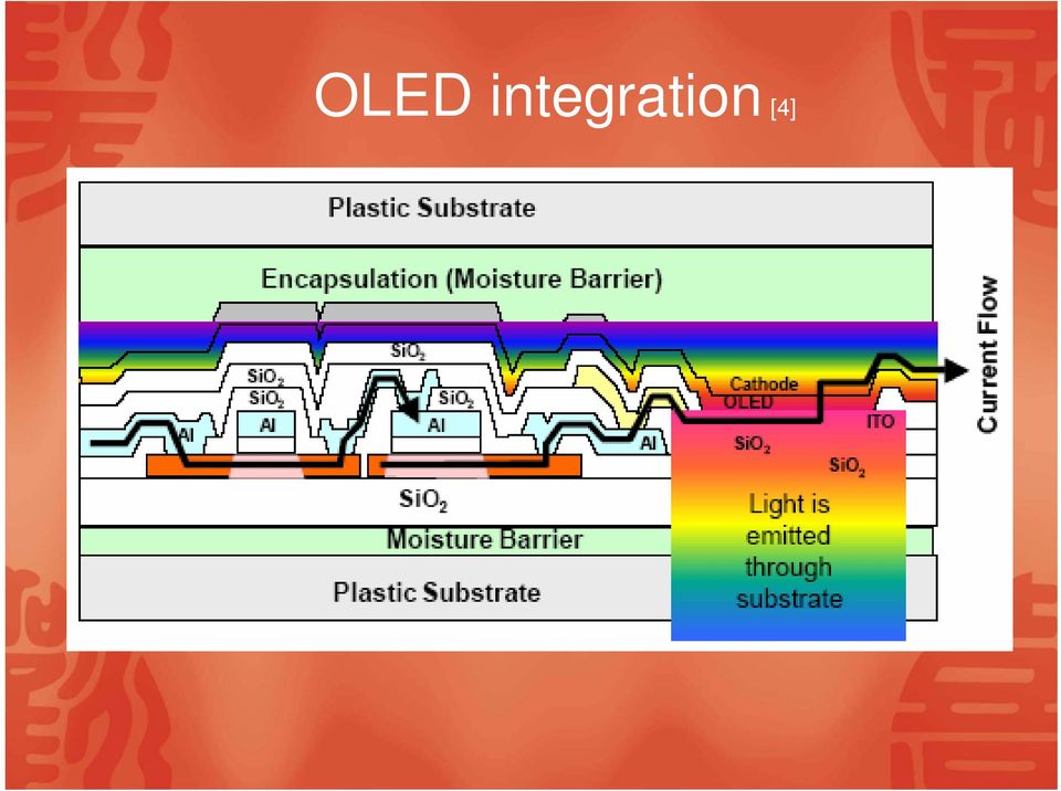
17 Fabrication challenges [4] Evaluate damage to plastic & thin films Defects generation during thin film deposition

18 References 1. S. M. Kelly, Flat Panel Displays, p. 141, W.J. Lee, Y.K. Fang, Hsin-Che Chiang, S.F. Ting, S.F. Chen, W.R. Chang, C.Y. Lin, T.Y. Lin, W.D. Wang, S.C. Hou, Jyh-Jier Ho, Solid- State Electronics 47 (2003) Clark W. Crawford, Organic Light Emitting Diodes Have Bright Future in Flat Panel Displays, Technology Commercialization Alliance, Daniel T., Teruo S., Sunder R., Patrick M. S., Paul G. C., and Paul W., Active Matrix OLED Display Backplanes on Flexible Substrates, FlexICs, Inc.,2002

OLED - Technologie der Zukunft
 OLED - Technologie der Zukunft Dr. Manfred Weigand MERCK KGaA, Darmstadt, Germany Cleanzone 2014 Cathode Ray Tube (CRT) Source: Peter Littmann Source: Patrick Schindler Source: Bundesarchiv, Bild 183-H0812-0031-001
Introduction OLEDs OTFTs OPVC Summary. Organic Electronics. Felix Buth. Walter Schottky Institut, TU München. Joint Advanced Student School 2008
 Felix Buth Joint Advanced Student School 2008 Outline 1 Introduction Difference organic/inorganic semiconductors From molecular orbitals to the molecular crystal 2 Organic Light Emitting Diodes Basic Principals
OLED: A New Display Technology Aditi Khazanchi,Akshay Kanwar, LOVENISH SALUJA, AAKASH DAMARA,VIKAS DAMARA
 www.ijecs.in International Journal Of Engineering And Computer Science ISSN:2319-7242 Volume1 Issue 2 Nov 2012 Page No. 75-84 OLED: A New Display Technology Aditi Khazanchi,Akshay Kanwar, LOVENISH SALUJA,
OLED Fabrication for Use in Display Systems
 OLED Fabrication for Use in Display Systems Chris Summitt Optical Sciences Center, University of Arizona, 1630 E University Blvd, Tucson, AZ 85721 [email protected] Abstract: Organic light-emitting
Ultra-high Barrier Plastic. MSE5420 Flexible Electronics Martin Yan, GE Global Research
 Ultra-high Barrier Plastic MSE5420 Flexible Electronics Martin Yan, GE Global Research Outline Introduction to plastic substrate and need for barrier Barrier technologies WVTR measurement technologies
Philips Lumiblade The World of OLED Lighting
 Philips Lumiblade The World of OLED Lighting Philips Lumiblade The World of OLED Lighting Content What are OLEDs? Benefits of OLEDs Realised Projects Application Areas The Future OLEDs What is OLED? OLED
OLED Status quo and Merck s position
 OLED Status quo and Merck s position Merck Information Day 2013 A Deep Dive into Merck s LC&OLED Business Dr. Udo Heider Vice President OLED Darmstadt, Germany June 26, 2013 Disclaimer Remarks All comparative
Introduction to VLSI Fabrication Technologies. Emanuele Baravelli
 Introduction to VLSI Fabrication Technologies Emanuele Baravelli 27/09/2005 Organization Materials Used in VLSI Fabrication VLSI Fabrication Technologies Overview of Fabrication Methods Device simulation
Introduction to OLED technology 1. General characteristics
 www.osram-oled.com Introduction to OLED technology 1. General characteristics 1.1. Structure An organic light-emitting diode (OLED) consists of several semiconducting organic layers sandwiched between
Organic semiconductors
 Plastic (Organic) Solar Cells: Accomplishments, Challenges, and Strategies Sumit Chaudhary Assistant Professor Department of Electrical and Computer Engineering Materials Science and Engineering Iowa State
Coating Technology: Evaporation Vs Sputtering
 Satisloh Italy S.r.l. Coating Technology: Evaporation Vs Sputtering Gianni Monaco, PhD R&D project manager, Satisloh Italy 04.04.2016 V1 The aim of this document is to provide basic technical information
Displays. Cathode Ray Tube. Semiconductor Elements. Basic applications. Oscilloscope TV Old monitors. 2009, Associate Professor PhD. T.
 Displays Semiconductor Elements 1 Cathode Ray Tube Basic applications Oscilloscope TV Old monitors 2 1 Idea of Electrostatic Deflection 3 Inside an Electrostatic Deflection Cathode Ray Tube Gun creates
Conductivity of silicon can be changed several orders of magnitude by introducing impurity atoms in silicon crystal lattice.
 CMOS Processing Technology Silicon: a semiconductor with resistance between that of conductor and an insulator. Conductivity of silicon can be changed several orders of magnitude by introducing impurity
Organic Light Emitting Diodes (OLED)
") 1 Organic Light Emitting Diodes (OLED) Karlheinz Blankenbach Pforzheim University, Germany Prof. Dr. Karlheinz Blankenbach Pforzheim University Tiefenbronner Str. 65 D-75175 Pforzheim, Germany Phone :
1 Organic Light Emitting Diodes (OLED) Karlheinz Blankenbach Pforzheim University, Germany Prof. Dr. Karlheinz Blankenbach Pforzheim University Tiefenbronner Str. 65 D-75175 Pforzheim, Germany Phone :
AN900 APPLICATION NOTE
 AN900 APPLICATION NOTE INTRODUCTION TO SEMICONDUCTOR TECHNOLOGY INTRODUCTION by Microcontroller Division Applications An integrated circuit is a small but sophisticated device implementing several electronic
Current Limiting Power Resistors for High-Power LED Module Lighting Applications
 Current Limiting Power Resistors for High-Power LED Module Lighting Applications PWR263 An ongoing trend toward miniaturization of virtually all electronics is accompanied by the demand for a reduction
Materials for Organic Electronic. Jeremy Burroughes FRS FREng
 Materials for Organic Electronic Applications Jeremy Burroughes FRS FREng Introduction Organic Thin Film Transistors Organic Solar Cells and Photodiodes All Printed OLED Summary 4k2k 56 Displays Panasonic
An organic semiconductor is an organic compound that possesses similar
 MSE 542 Final Term Paper Title: Organic Semiconductor for Flexible Electronics Name: Chunhung Huang Introduction: An organic semiconductor is an organic compound that possesses similar properties to inorganic
Light management for photovoltaics. Ando Kuypers, TNO Program manager Solar
 Light management for photovoltaics Ando Kuypers, TNO Program manager Solar Global energy consumption: 500 ExaJoule/Year Solar irradiation on earth sphere: 5.000.000 ExaJoule/year 2 Capturing 0,01% covers
Hyun Jae Kim. Yonsei University
 Recent development in Electronic Paper Technology Hyun Jae Kim Yonsei University [email protected] kr Do you remember what it was like 25 years ago? Motorola DynaTAC 8000X Some quick facts LG PRADA 1,305
2. Deposition process
 Properties of optical thin films produced by reactive low voltage ion plating (RLVIP) Antje Hallbauer Thin Film Technology Institute of Ion Physics & Applied Physics University of Innsbruck Investigations
Amorphous Silicon Backplane with Polymer MEMS Structures for Electrophoretic Displays
 Amorphous Silicon Backplane with Polymer MEMS Structures for Electrophoretic Displays J.H. Daniel 1, a, B.S. Krusor 1, N. Chopra 2, R.A. Street 1, P.M. Kazmaier 2, S.E. Ready 1, J.H. Ho 1 1 Palo Alto Research
Vacuum Evaporation Recap
 Sputtering Vacuum Evaporation Recap Use high temperatures at high vacuum to evaporate (eject) atoms or molecules off a material surface. Use ballistic flow to transport them to a substrate and deposit.
For Touch Panel and LCD Sputtering/PECVD/ Wet Processing
 production Systems For Touch Panel and LCD Sputtering/PECVD/ Wet Processing Pilot and Production Systems Process Solutions with over 20 Years of Know-how Process Technology at a Glance for Touch Panel,
Physics 441/2: Transmission Electron Microscope
 Physics 441/2: Transmission Electron Microscope Introduction In this experiment we will explore the use of transmission electron microscopy (TEM) to take us into the world of ultrasmall structures. This
Low-cost Printed Electronic Nose Gas Sensors for Distributed Environmental Monitoring
 Low-cost Printed Electronic Nose Gas Sensors for Distributed Environmental Monitoring Vivek Subramanian Department of Electrical Engineering and Computer Sciences University of California, Berkeley RD83089901
The Physics of Energy sources Renewable sources of energy. Solar Energy
 The Physics of Energy sources Renewable sources of energy Solar Energy B. Maffei [email protected] Renewable sources 1 Solar power! There are basically two ways of using directly the radiative
Implementation Of High-k/Metal Gates In High-Volume Manufacturing
 White Paper Implementation Of High-k/Metal Gates In High-Volume Manufacturing INTRODUCTION There have been significant breakthroughs in IC technology in the past decade. The upper interconnect layers of
MOS (metal-oxidesemiconductor) 李 2003/12/19
 李 2003/12/19") MOS (metal-oxidesemiconductor) 李 2003/12/19 Outline Structure Ideal MOS The surface depletion region Ideal MOS curves The SiO 2 -Si MOS diode (real case) Structure A basic MOS consisting of three layers.
MOS (metal-oxidesemiconductor) 李 2003/12/19 Outline Structure Ideal MOS The surface depletion region Ideal MOS curves The SiO 2 -Si MOS diode (real case) Structure A basic MOS consisting of three layers.
Etching Etch Definitions Isotropic Etching: same in all direction Anisotropic Etching: direction sensitive Selectivity: etch rate difference between
 Etching Etch Definitions Isotropic Etching: same in all direction Anisotropic Etching: direction sensitive Selectivity: etch rate difference between 2 materials Other layers below one being etch Masking
Cree XLamp MX-6 LEDs Data Sheet
 Cree XLamp MX-6 LEDs Data Sheet The Cree XLamp MX-6 LED provides the proven lighting-class performance and reliability of Cree XLamp LEDs in a flat-top PLCC package. The XLamp MX-6 LED continues Cree s
6.772/SMA5111 - Compound Semiconductors Lecture 18 - Light Emitting Diodes - Outline
 6.772/SMA5111 - Compound Semiconductors Lecture 18 - Light Emitting Diodes - Outline Recombination Processes (continued from Lecture 17) Radiative vs. non-radiative Relative carrier lifetimes Light emitting
Discontinued. LUXEON V Portable. power light source. Introduction
 Preliminary Technical Datasheet DS40 power light source LUXEON V Portable Introduction LUXEON is a revolutionary, energy efficient and ultra compact new light source, combining the lifetime and reliability
Solar Photovoltaic (PV) Cells
 Cells") Solar Photovoltaic (PV) Cells A supplement topic to: Mi ti l S Micro-optical Sensors - A MEMS for electric power generation Science of Silicon PV Cells Scientific base for solar PV electric power generation
Solar Photovoltaic (PV) Cells A supplement topic to: Mi ti l S Micro-optical Sensors - A MEMS for electric power generation Science of Silicon PV Cells Scientific base for solar PV electric power generation
Types of Epitaxy. Homoepitaxy. Heteroepitaxy
 Epitaxy Epitaxial Growth Epitaxy means the growth of a single crystal film on top of a crystalline substrate. For most thin film applications (hard and soft coatings, optical coatings, protective coatings)
X-ray Imaging Systems
 Principles of Imaging Science I (RAD 119) X-ray Tube & Equipment X-ray Imaging Systems Medical X-ray Equipment Classified by purpose or energy/current levels kvp, ma Radiographic Non-dynamic procedures
Edixeon S5 White Series Datasheet
 Edixeon S5 White Series Datasheet Edixeon Series Features : Various colors for choice Low voltage operation Instant light Long operating life Reflow process compatible Copyright 2013 Edison Opto Corporation.
Laboratory #3 Guide: Optical and Electrical Properties of Transparent Conductors -- September 23, 2014
 Laboratory #3 Guide: Optical and Electrical Properties of Transparent Conductors -- September 23, 2014 Introduction Following our previous lab exercises, you now have the skills and understanding to control
TIE-31: Mechanical and thermal properties of optical glass
 PAGE 1/10 1 Density The density of optical glass varies from 239 for N-BK10 to 603 for SF66 In most cases glasses with higher densities also have higher refractive indices (eg SF type glasses) The density
Fabrication and Characterization of N- and P-Type a-si:h Thin Film Transistors
 Fabrication and Characterization of N- and P-Type a-si:h Thin Film Transistors Engineering Practical Jeffrey Frederick Gold Fitzwilliam College University of Cambridge Lent 1997 FABRCATON AND CHARACTERZATON
High Rate Oxide Deposition onto Web by Reactive Sputtering from Rotatable Magnetrons
 High Rate Oxide Deposition onto Web by Reactive Sputtering from Rotatable Magnetrons D.Monaghan, V. Bellido-Gonzalez, M. Audronis. B. Daniel Gencoa, Physics Rd, Liverpool, L24 9HP, UK. www.gencoa.com,
High Resolution Spatial Electroluminescence Imaging of Photovoltaic Modules
 High Resolution Spatial Electroluminescence Imaging of Photovoltaic Modules Abstract J.L. Crozier, E.E. van Dyk, F.J. Vorster Nelson Mandela Metropolitan University Electroluminescence (EL) is a useful
3.0mm (1.2") 8 8 Hyper Red Dot Matrix LED Displays Technical Data Sheet. Model No.: KWM-30881XVB
 8 8 Hyper Red Dot Matrix LED Displays Technical Data Sheet. Model No.: KWM-30881XVB") .mm (.") Hyper Red Dot Matrix LED Displays Technical Data Sheet Model No.: KWM-XVB Spec No: WA/B Rev No: V. Date:Sep// Page of Features:.inch (.mm) Matrix height. Colors: Hyper Red. Flat package and light
.mm (.") Hyper Red Dot Matrix LED Displays Technical Data Sheet Model No.: KWM-XVB Spec No: WA/B Rev No: V. Date:Sep// Page of Features:.inch (.mm) Matrix height. Colors: Hyper Red. Flat package and light
How compact discs are made
 How compact discs are made Explained by a layman for the laymen By Kevin McCormick For Science project at the Mountain View Los Altos High School Abstract As the major media for music distribution for
LZC-00MC40. LedEngin, Inc. High Luminous Efficacy RGB LED Emitter. Key Features. Typical Applications. Description
 Key Features High Luminous Efficacy RGB LED Emitter LZC-MC4 Ultra-bright, Ultra-compact 4W RGB LED Full spectrum of brilliant colors with superior color mixing Small high density foot print 9.mm x 9.mm
Semiconductor doping. Si solar Cell
 Semiconductor doping Si solar Cell Two Levels of Masks - photoresist, alignment Etch and oxidation to isolate thermal oxide, deposited oxide, wet etching, dry etching, isolation schemes Doping - diffusion/ion
Injection molding equipment
 Injection Molding Process Injection molding equipment Classification of injection molding machines 1. The injection molding machine processing ability style clamping force(kn) theoretical injection volume(cm3)
Good Boards = Results
 Section 2: Printed Circuit Board Fabrication & Solderability Good Boards = Results Board fabrication is one aspect of the electronics production industry that SMT assembly engineers often know little about.
Excerpt Direct Bonded Copper
 xcerpt irect Bonded Copper Presented by ouglas C. Hopkins, Ph.. 312 Bonner Hall University at Buffalo Buffalo, Y 14620-1900 607-729-9949, fax: 607-729-7129 Authors thank Curamik lectronics A member of
SPECIFICATION. PART NO. : MT0380-UV-A 5.0mm ROUND LED LAMP. 3Northway Lane North Latham,New York 12110.
 3Northway Lane North Latham,New York 12110. Tollfree:1.800.984.5337 Phone:1.518.956.2980 Fax:1.518.785.4725 Http://www.marktechopto.com SPECIFICATION PART NO. : MT0380-UV-A LAMP ATTENTION OBSERVE PRECAUTION
JD(Doug) Rooks Western Area Applications Manager
 Rooks Western Area Applications Manager") AC vs DC LED Design/Benefits JD(Doug) Rooks Western Area Applications Manager Seoul Semiconductor Product Summary Acriche Side View LED Dot Matrix Z-Power LED Chip LED Lamp LED Custom Display Deep UV Top
AC vs DC LED Design/Benefits JD(Doug) Rooks Western Area Applications Manager Seoul Semiconductor Product Summary Acriche Side View LED Dot Matrix Z-Power LED Chip LED Lamp LED Custom Display Deep UV Top
Luckylight. 3.0mm (1.2") 8 8 Super Yellow Dot Matrix LED Displays Technical Data Sheet. Model No.: KWM-30881XUYB
 8 8 Super Yellow Dot Matrix LED Displays Technical Data Sheet. Model No.: KWM-30881XUYB") 3.mm (.") 8 8 Super Yellow Dot Matrix LED Displays Technical Data Sheet Model No.: KWM-388XUYB Spec No: W88A/B Rev No: V. Date:Sep/3/8 Page: OF 6 Features:.inch (3.mm) Matrix height. Colors: Super Yellow.
3.mm (.") 8 8 Super Yellow Dot Matrix LED Displays Technical Data Sheet Model No.: KWM-388XUYB Spec No: W88A/B Rev No: V. Date:Sep/3/8 Page: OF 6 Features:.inch (3.mm) Matrix height. Colors: Super Yellow.
Electronics and Soldering Notes
 Electronics and Soldering Notes The Tools You ll Need While there are literally one hundred tools for soldering, testing, and fixing electronic circuits, you only need a few to make robot. These tools
Available in white (2,600 K to 8,300 K CCT) Maximum drive current: 1000 ma. Wide viewing angle: 120. Electrically neutral thermal path
 Maximum drive current: 1000 ma. Wide viewing angle: 120. Electrically neutral thermal path") PRODUCT FAMILY DATA SHEET CLD-23 REV 3 Cree XLamp MX-6 LEDs PRODUCT DESCRIPTION The Cree XLamp MX-6 LED provides the proven lighting-class performance and reliability of Cree XLamp LEDs in a flat-top PLCC
PRODUCT FAMILY DATA SHEET CLD-23 REV 3 Cree XLamp MX-6 LEDs PRODUCT DESCRIPTION The Cree XLamp MX-6 LED provides the proven lighting-class performance and reliability of Cree XLamp LEDs in a flat-top PLCC
LEAD CRYSTAL. User Manual. Valve-regulated lead-crystal batteries Energy storage Cells
 Engineering Production Sales LEAD CRYSTAL Valve-regulated lead-crystal batteries Energy storage Cells User Manual www.axcom-battery-technology.de [email protected] Chapter 1: 1. Introduction
Graphical displays are generally of two types: vector displays and raster displays. Vector displays
 Display technology Graphical displays are generally of two types: vector displays and raster displays. Vector displays Vector displays generally display lines, specified by their endpoints. Vector display
TV Display Innovation History from CRT to OLED Technology
 TV Display Innovation History from CRT to OLED Technology TV has become an important part of our everyday life. How was early TV display technology different from current technologies? How will our TV
Optical Hyperdoping: Transforming Semiconductor Band Structure for Solar Energy Harvesting
 Optical Hyperdoping: Transforming Semiconductor Band Structure for Solar Energy Harvesting 3G Solar Technologies Multidisciplinary Workshop MRS Spring Meeting San Francisco, CA, 5 April 2010 Michael P.
VLSI Fabrication Process
 VLSI Fabrication Process Om prakash 5 th sem ASCT, Bhopal [email protected] Manisha Kumari 5 th sem ASCT, Bhopal [email protected] Abstract VLSI stands for "Very Large Scale Integration". This
Solid State Detectors = Semi-Conductor based Detectors
 Solid State Detectors = Semi-Conductor based Detectors Materials and their properties Energy bands and electronic structure Charge transport and conductivity Boundaries: the p-n junction Charge collection
Multi-LED Package design, fabrication and thermalanalysis
 Multi-LED Package design, fabrication and thermalanalysis R.H. Poelma 1, S. Tarashioon 1, H.W. van Zeijl 1, S. Goldbach 2, J.L.J. Zijl 3 and G.Q. Zhang 1,2 1 Delft University of Technology, Delft, The
SLLP-5630-150-G PRODUCT DATASHEET. RoHS Compliant
 PRODUCT DATASHEET SLLP-5630-150-G Table of Contents Features... 1 Applications 1 Characteristics.. 1 Typical Electro optical Characteristics Curves... 3 Mechanical Dimensions... 4 Carrier Tape Dimensions.....
DNA Separation Methods. Chapter 12
 DNA Separation Methods Chapter 12 DNA molecules After PCR reaction produces many copies of DNA molecules Need a way to separate the DNA molecules from similar sized molecules Only way to genotype samples
Flat Panel Displays How does a Flat Panel Display work? Flat Panel Displays
 Flat Panel Displays When talking about computer monitors, the word on the street is that thin is in. For example, at this year s Comdex Fall '98, the computer industry's largest North American tradeshow,
Figure 1 Wafer with Notch
 Glass Wafer 2 SCHOTT is an international technology group with more than 125 years of experience in the areas of specialty glasses, materials and advanced technologies. With our high-quality products and
PIEZOELECTRIC FILMS TECHNICAL INFORMATION
 PIEZOELECTRIC FILMS TECHNICAL INFORMATION 1 Table of Contents 1. PIEZOELECTRIC AND PYROELECTRIC EFFECTS 3 2. PIEZOELECTRIC FILMS 3 3. CHARACTERISTICS PROPERTIES OF PIEZOELECTRIC FILMS 3 4. PROPERTIES OF
703-0148 InGaN / Sapphire White Water clear. Parameter Rating Unit
 Package Dimensions: * All dimensions are in mm * Tolerance: ±.6mm unless otherwise noted. LED Chip Lens Colour Ant Part No. Material Colour Coordinates 73-148 InGaN / Sapphire White Water clear Absolute
Barrier Coatings: Conversion and Production Status
 Transparent SiO 2 Barrier Coatings: Conversion and Production Status E. Finson and J. Felts, Airco Coating Technology, Concord, CA Keywords: Permeation barrier coatings; Reactive evaporation; SiO 2 ABSTRACT
Chapter 5: Diffusion. 5.1 Steady-State Diffusion
 : Diffusion Diffusion: the movement of particles in a solid from an area of high concentration to an area of low concentration, resulting in the uniform distribution of the substance Diffusion is process
T H A N K S F O R A T T E N D I N G OUR. FLEX-RIGID PCBs. Presented by: Nechan Naicker
 T H A N K S F O R A T T E N D I N G OUR TECHNICAL WEBINAR SERIES FLEX-RIGID PCBs Presented by: Nechan Naicker We don t just sell PCBs. We sell sleep. Cirtech EDA is the exclusive SA representative of the
Specification MBT801-S
 Specification MBT801S Drawn SSC Approval 고객명 Approval.com MBT801S 1. Features 2. Absolute Maximum Ratings 3. Electro Characteristics 4. Optical characteristics 5. Outline Dimension 6. Packing 7. Soldering
High power picosecond lasers enable higher efficiency solar cells.
 White Paper High power picosecond lasers enable higher efficiency solar cells. The combination of high peak power and short wavelength of the latest industrial grade Talisker laser enables higher efficiency
Crystallization of Amorphous Silicon Using Xenon Flash Lamp Annealing
 Crystallization of Amorphous Silicon Using Xenon Flash Lamp Annealing Henry Hellbusch 2/5/2016 RIT - Corning - Crystallization of A-Si with FLA 1 Purpose Thin Film Transistors (TFT) on glass are utilized
Luckylight. 60.20mm (2.4") 8 8 RGB color Dot Matrix LED Displays Technical Data Sheet. Model No.: KWM-50884XRGBB
 8 8 RGB color Dot Matrix LED Displays Technical Data Sheet. Model No.: KWM-50884XRGBB") 6.2mm (2.4") RGB color Dot Matrix LED Displays Technical Data Sheet Model No.: KWM-54XRGBB Spec No: W23A/BRGB Rev No: V.2 Date:Sep//29 Page: OF 9 Features: 2.4inch (6.2mm) digit height. Excellent segment
6.2mm (2.4") RGB color Dot Matrix LED Displays Technical Data Sheet Model No.: KWM-54XRGBB Spec No: W23A/BRGB Rev No: V.2 Date:Sep//29 Page: OF 9 Features: 2.4inch (6.2mm) digit height. Excellent segment
Chapter 2 The Study on Polycrystalline Pentacene Thin Film Transistors
 Chapter 2 The Study on Polycrystalline Pentacene Thin Film Transistors 2.1 Introduction Recent focus and attention on organic thin film transistors (TFTs) resulted in dramatic performance improvements
Radiation Curable Components and Their use in Hard, Scratch Resistant Coating Applications
 Radiation Curable Components and Their use in Hard, Scratch Resistant Coating Applications William Schaeffer Steven Tyson Indu Vappala Robert Kensicki Sartomer USA, LLC 502 Thomas Jones Way Exton, PA 19343
Efficient and reliable operation of LED lighting is dependent on the right choice of current-limiting resistor
 Efficient and reliable operation of LED lighting is dependent on the right choice of current-limiting resistor Phil Ebbert, VP of Engineering, Riedon Inc. Introduction Not all resistors are the same and
Hello and Welcome to this presentation on LED Basics. In this presentation we will look at a few topics in semiconductor lighting such as light
 Hello and Welcome to this presentation on LED Basics. In this presentation we will look at a few topics in semiconductor lighting such as light generation from a semiconductor material, LED chip technology,
07 21 19 Guide Specification STAYFLEX CORROSION CONTROL AND THERMAL INSULATION SYSTEM
 07 21 19 STAYFLEX CORROSION CONTROL AND THERMAL INSULATION SYSTEM 7819 Broadview Road Cleveland, OH 44131 800-522-4522 February, 2011 SPEC NOTE: This guide specification is intended for use when specifying
Soldering of SMD Film Capacitors in Practical Lead Free Processes
 Soldering of SMD Film Capacitors in Practical Lead Free Processes Matti Niskala Product Manager, SMD products Evox Rifa Group Oyj, a Kemet Company Lars Sonckin kaari 16, 02600 Espoo, Finland Tel: + 358
Lecture 12. Physical Vapor Deposition: Evaporation and Sputtering Reading: Chapter 12. ECE 6450 - Dr. Alan Doolittle
 Lecture 12 Physical Vapor Deposition: Evaporation and Sputtering Reading: Chapter 12 Evaporation and Sputtering (Metalization) Evaporation For all devices, there is a need to go from semiconductor to metal.
Computer Peripherals
 Computer Peripherals School of Computer Engineering Nanyang Technological University Singapore These notes are part of a 3rd year undergraduate course called "Computer Peripherals", taught at Nanyang Technological
Ultra-High Density Phase-Change Storage and Memory
 Ultra-High Density Phase-Change Storage and Memory by Egill Skúlason Heated AFM Probe used to Change the Phase Presentation for Oral Examination 30 th of May 2006 Modern Physics, DTU Phase-Change Material
Product family data sheet
 Cree XLamp MX-6 LEDs Product family data sheet CLD-DS23 Rev 3A Product Description The Cree XLamp MX-6 LED provides the proven lightingclass performance and reliability of Cree XLamp LEDs in a flat-top
Cree XLamp MX-3S LEDs Data Sheet
 Cree XLamp MX-3S LEDs Data Sheet The Cree XLamp MX-3S LED provides the proven lighting-class performance and reliability of Cree XLamp LEDs in a high voltage, PLCC configuration. All members of the MX-family
rred.com ieverred.com
 1Features/ Emitting Color/Green/ Lens Type/Water Clear/ Device Outline/3.52.81.9mm RoHS compliant/ RoHS 2Applications/ Backlight for MobileMachine Vision LCD Display/ Backlight in Dashboard and switch
PRDUCT SPECIFICATON TFT LCD MODULE Model : ELT240320ATP
 PRDUCT SPECIFICATON TFT LCD MODULE Model : ELT240320ATP 2.8 inch TFT LCD with Touch Screen This specification is subject to change without notice. 2 Contents Page 1. LCM Specification.....3 2. Functional
Improved Contact Formation for Large Area Solar Cells Using the Alternative Seed Layer (ASL) Process
 Process") Improved Contact Formation for Large Area Solar Cells Using the Alternative Seed Layer (ASL) Process Lynne Michaelson, Krystal Munoz, Jonathan C. Wang, Y.A. Xi*, Tom Tyson, Anthony Gallegos Technic Inc.,
Improved Contact Formation for Large Area Solar Cells Using the Alternative Seed Layer (ASL) Process Lynne Michaelson, Krystal Munoz, Jonathan C. Wang, Y.A. Xi*, Tom Tyson, Anthony Gallegos Technic Inc.,
Influence of Belt Furnace on Glass-to-Metal Seal Process
 Influence of Belt Furnace on Glass-to-Metal Seal Process Introduction The glass, under suitable conditions, will bond well to a wide variety of metals and alloys which has led to the development of many
Everline Module Application Note: Round LED Module Thermal Management
 Everline Module Application Note: Round LED Module Thermal Management PURPOSE: Use of proper thermal management is a critical element of Light Emitting Diode (LED) system design. The LED temperature directly
THIN-FILM SILICON SOLAR CELLS
 ENGINEERING SCIENCES Micro- and Nanotechnology THIN-FILM SILICON SOLAR CELLS Arvind Shah, Editor The main authors of Thin-Film Silicon Solar Cells are Christophe Ballif, Wolfhard Beyer, Friedhelm Finger,
Application Note 142 August 2013. New Linear Regulators Solve Old Problems AN142-1
 August 2013 New Linear Regulators Solve Old Problems Bob Dobkin, Vice President, Engineering and CTO, Linear Technology Corp. Regulators regulate but are capable of doing much more. The architecture of
3.0*3.0mm (1.2") 8 8 Super Yellow Dot Matrix LED Displays Technical Data Sheet. Model No.: KWM-R30881XUYB
 8 8 Super Yellow Dot Matrix LED Displays Technical Data Sheet. Model No.: KWM-R30881XUYB") 3.*3.mm (.2") 8 8 Super Yellow Dot Matrix LED Displays Technical Data Sheet Model No.: KWM-R388XUYB Spec No: W288A/B Rev No: V.2 Date: Sep/8/27 Page: OF 6 Features:.2inch (3.7mm) Matrix height. Colors:Super
3.*3.mm (.2") 8 8 Super Yellow Dot Matrix LED Displays Technical Data Sheet Model No.: KWM-R388XUYB Spec No: W288A/B Rev No: V.2 Date: Sep/8/27 Page: OF 6 Features:.2inch (3.7mm) Matrix height. Colors:Super
Graphene a material for the future
 Graphene a material for the future by Olav Thorsen What is graphene? What is graphene? Simply put, it is a thin layer of pure carbon What is graphene? Simply put, it is a thin layer of pure carbon It has
Robert G. Hunsperger. Integrated Optics. Theory and Technology. Fourth Edition. With 195 Figures and 17 Tables. Springer
 Robert G. Hunsperger Integrated Optics Theory and Technology Fourth Edition With 195 Figures and 17 Tables Springer Contents 1. Introduction 1 1.1 Advantages of Integrated Optics 2 1.1.1 Comparison of
HOT BAR REFLOW SOLDERING FUNDAMENTALS. A high quality Selective Soldering Technology
 HOT BAR REFLOW SOLDERING FUNDAMENTALS A high quality Selective Soldering Technology Content 1. Hot Bar Reflow Soldering Introduction 2. Application Range 3. Process Descriptions > Flex to PCB > Wire to
The MOSFET Transistor
 The MOSFET Transistor The basic active component on all silicon chips is the MOSFET Metal Oxide Semiconductor Field Effect Transistor Schematic symbol G Gate S Source D Drain The voltage on the gate controls