µpfc ONE CYCLE CONTROL PFC IC
|
|
|
- Ira Poole
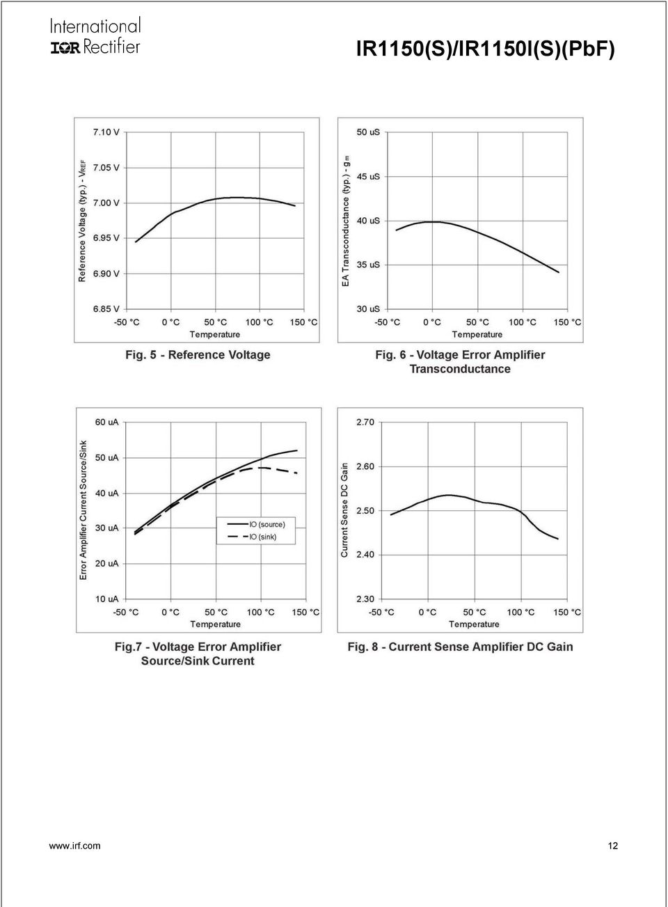
- 9 years ago
- Views:
Transcription
1 Features PFC with IR proprietary One Cycle Control Continuous conduction mode (CCM) boost type PFC No line voltage sense required Programmable switching frequency (50kHz-200kHz) Programmable output overvoltage protection Brownout and output undervoltage protection Cycle-by-cycle peak current limit Soft start User initiated micropower Sleep Mode Data Sheet No. PD60230 revd IR1150(S)(PbF) IR1150I(S)(PbF) µpfc ONE CYCLE CONTROL PFC IC Open loop protection Maximum duty cycle limit of 98% User programmable fixed frequency operation Min. off time of ns over freq range VCC under voltage lockout Internally clamped 13V gate drive Fast 1.5A peak gate drive Micropower startup (<200 µa) Latch immunity and ESD protection Parts also available Lead-Free Description The µpfc IR1150 is a power factor correction (PFC) control IC designed to operate in continuous conduction mode (CCM) over a wide range input line voltages. The IR1150 is based on IR's proprietary "One Cycle Control" (OCC) technique providing a cost effective solution for PFC. The proprietary control method allows major reductions in component count, PCB area and design time while delivering the same high system performance as traditional solutions. The IC is fully protected and eliminates the often noise sensitive line voltage sensing requirements of existing solutions. The IR1150 features include programmable switching frequency, programmable dedicated over voltage protection, soft start, cycle- by-cycle peak current limit, brownout, open loop, UVLO and micropower startup current. In addition, for low standby power requirements (Energy Star, 1W Standby, Blue Angel, etc.), the IC can be driven into sleep mode with total current consumption below 200µA, by pulling the OVP pin below 0.62V. Packages 8-Lead SOIC 8-Lead PDIP 1

2 Absolute Maximum Ratings Absolute maximum ratings indicate sustained limits beyond which damage to the device may occur. All voltages are absolute voltages referenced to COM. Thermal resistance and power dissipation are measured under board mounted and still air conditions. Parameters Symbols Min. Max. Units Remarks VCC voltage V CC V Not internally clamped Freq. voltage V FREQ V ISNS voltage V ISNS V OVP/EN voltage V OVP/EN V VFB voltage V FB V COMP voltage V COMP V Gate voltage V GATE V Continuous gate current I GATE -5 5 ma Max peak gate current I GATEPK A Junction temperature T J C Storage temperature T S C Thermal resistance R θ JA 128 C/W SOIC-8 84 C/W PDIP-8 Package power dissipation P D 675 mw SOIC-8 T AMB = 25 C 1000 mw PDIP-8 T AMB = 25 C ESD protection V ESD 2 kv Human body model* Recommended Operating Conditions Recommended operating conditions for reliable operation with margin Supply voltage VCC V Junction temperature TJ C Ambient temperature TA 0 70 C IR1150(S) Ambient temperature TA C IR1150I(S) Switching frequency FSW khz Electrical Characteristics The electrical characteristics involve the spread of values guaranteed within the specified supply voltage and junction temperature range T J from 25 C to 125 C. Typical values represent the median values, which are related to 25 C. If not otherwise stated, a supply voltage of V CC =15V is assumed for test condition Supply Section VCC turn-on threshold VCC ON V VCC turn-off threshold (under voltage lock out) VCC UVLO V *Per EIA/JESD22-A114-B (discharging a 100pF capacitor through a 1.5KΩ series resistor) 2

3 Electrical Characteristics cont. The electrical characteristics involve the spread of values guaranteed within the specified supply voltage and junction temperature range T J from 25 C to 125 C. Typical values represent the median values, which are related to 25 C. If not otherwise stated, a supply voltage of V CC =15V is assumed for test condition. VCC turn-off hysteresis V CC HYST V ma C LOAD =1nF f SW =200kHZ ma C LOAD =10nF f SW =200kHZ Operating current I CC Standby mode - inactive gate 8 10 ma Internal oscillator running Startup current I CCSTART 175 ua V CC =V CC ON - 0.1V Sleep current I SLEEP ua V OVP <0.5V, V CC =15V Sleep threshold V SLEEP V Oscillator Section Switching frequency f SW khz R SET = 165kΩ-37kΩ approx. Initial accuracy f SW ACC 5 % T A = 25 C Voltage stability V STAB % 13V <VCC <20V Temperature stability T STAB 2 % -25 C TJ 125 C Total variation f VT 10 % Line & temperature Long term stability F STABLT % T AMB = 125 C, 1000Hrs Maximum duty cycle D MAX % f SW =200kHz Minimum duty cycle D MIN 0 % Minimum off time T offmin Ns f SW = 50kHz to 200kHz Protection Section Open loop protection(olp) Vfb threshold Output under voltage protection (OUV) V OLP %VREF V OUV %VREF Brown out protection Output over voltage protection (OVP) V OVP %VREF OVP hysteresis mv Peak current limit protection (I PKLMT ) I SNS voltage threshold V ISNS V 3

4 Internal Voltage Reference Section Reference voltage V REF V T A = 25 C Line regulation R REG mv 13.5V <V CC < 20V Temp stability T STAB 0.4 % -25 C T AMB 125 C Total variation V TOT V Over V CC and T j ranges Voltage Error Amplifier Section Transconductance g m µs -25 C T AMB 125 C Source/sink current Soft start delay time (calculated) I OVEA µa t ss 40 ms VCOMP voltage (fault) V COMP FLT V Effective VCOMP voltage V COMP EFF 6.05 V Input bias current I IB µa Open loop bandwidth BW 1 MHz Input offset voltage temp coefficient TC IOV 10 µv/ C Note 1 Common mode rejection ratio CMRR 100 db Output low voltage V OL 0.5 V Output high voltage V OH V VCOMP start voltage V COMP START mv Current Amplifier Section DC gain g DC 2.5 V/V Corner frequency f C khz Note 1 Input offset voltage V IO 1 4 mv Note 1 T AMB = 25 C -25 C T AMB 125 C R GAIN =1kΩ, C ZERO =0.33µF C POLE =0.01µF, 1mA (max) 25µA steady state V FB =0V -25 C T AMB 125 C ISNS bias current Ι IB µa V FB =0V,-25 C T AMB 125 C Input offset voltage temp coefficient TC IOV 10 µv/ C Note 1 Common mode rejection ratio CMRR 100 db Blanking time T BLANK ns T AMB = 25 C ns -25 C T AMB 125 C 4
 V COMP FLT 1.2 1.5 0.2 V Effective VCOMP voltage V COMP EFF 6.05 V Input bias current I IB -0.2-0.")
5 Gate Driver Section Gate low voltage V GLO V I GATE =200mA Gate high voltage V GTH V V CC =20V Gate high voltage V GTH 9.5 V V CC =11.5V Rise time Fall time tr tf 20 ns C LOAD = 1nF, V CC =16V 70 ns C LOAD = 10nF, V CC =16V 20 ns C LOAD = 1nF, V CC =16V 70 ns C LOAD = 10nF, V CC =16V Out peak current I OPK 1.5 A C LOAD = 10nF, V CC =16V Gate fault VG fault 1.8 V I GATE =20mA Note 1: Guaranteed by design, but not tested in production. 5

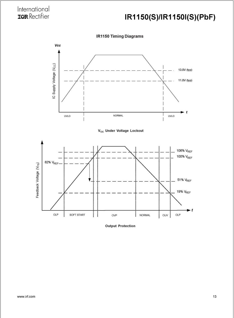
6 Block Diagram IR1150(S)/IR1150I(S)(PbF) 0.62V Lead Assignments & Definitions Lead Assignment Pin# Symbol Description 1 COM Ground 2 FREQ Frequency Set 3 I SNS Current Sense 4 OVP/EN Overvoltage Fault Detect / Enable 5 COMP Voltage Loop Compensation 6 V FB Output Voltage Sense 7 V CC IC Supply Voltage 8 GATE Gate Drive Output 6

7 General Description The µpfc IR1150 is intended for boost converters for power factor correction operating at a fixed frequency in continuous conduction mode. The IC operates with two loops; an inner current loop and an outer voltage loop. The inner current loop is fast, reliable and does not require sensing of the input voltage in order to create a current reference. This inner current loop sustains the sinusoidal profile of the average input current based on the dependency of the pulse width modulator duty cycle on the input line voltage in order to determine the analogous input line current. Thus, the current loop uses the embedded input voltage signal to control the average input current to follow the input voltage. The IR1150 enables excellent THD performance. In light load conditions, a small distortion occurs at zerocrossing due to the finite boost inductance but this is negligible and well within EN Class D specifications. The outer voltage loop controls the DC bus voltage. This voltage is fed into the voltage error amplifier to control the slope of the integrator ramp and sets the amplitude of the average input current. The two loops combine to control the amplitude, phase and shape of the input current, with respect to the input voltage, giving near-unity power factor. The IC is designed for robust operation and provides protection from system level over current, over voltage, under voltage, and brownout conditions. IC Supply The UVLO circuit monitors the VCC pin and maintains the gate drive signal inactive until the VCC pin voltage reaches the UVLO turn on threshold, (V CC ON ). As soon as the VCC voltage exceeds this threshold, provided that the V FB pin voltage is greater than 20%VREF, the gate drive will begin switching (under Soft Start) and increase the pulse width to its maximum value as demanded by the output voltage error amplifier. If the voltage on the VCC pin falls below the UVLO turn off threshold, (V CC UVLO ), the IC turns off, gate drive is terminated, and the turn on threshold must again be exceeded in order to re-start the process and move into Soft Start mode. Soft Start Soft Start controls the rate of rise of the output voltage error amplifier in order to obtain a linear control of the increasing duty cycle as a function of time. The Soft Start time is controlled by voltage error amplifier compensation components selected, and is user programmable based on desired loop crossover frequency. Frequency Select The switching frequency of the IC is programmable by an external resistor at the FREQ pin. The design incorporates min/max restrictions such that the minimum and maximum operating frequency fall within the range of kHz. Gate Drive The gate drive is a totem pole driver with 1.5A capability. If higher currents are required, additional external drivers can be used. 7

8 Detailed Pin Description COM: Ground This is the ground potential pin of the integrated control circuit. All internal devices are referenced to this point. V FB : Output Voltage Feedback The output voltage of the boost converter is sensed via a resistive divider and fed into this pin, which is the inverting input of the output voltage error amplifier. The impedance of the divider string must be low enough so as to not introduce substantial error due to the input bias currents of the amplifier, yet high enough so as to minimize power dissipation. A typical value of external divider impedance is 1MΩ. The error amplifier is a transconductance type which yields high output impedance, thus increasing the noise immunity of the error amplifier output. This also eliminates input divider string interaction with compensation feedback capacitors and reducing the loading of divider string due to a low impedance output of the amplifier. COMP: Voltage Loop Compensation External circuitry from this pin to ground compensates the system voltage loop and soft start time. This is the output of the voltage error amplifier. This pin will be discharged via internal resistance when a fault mode occurs. GATE: Gate Drive Output This is the gate drive output of the IC. Drive voltage is internally limited and provides ±1.5A peak with matched rise and fall times. FREQ: Frequency Set This is the user programmable frequency pin. An external resistor from this pin to the COM pin programs the frequency. The operational switching frequency range for the device is 50kHz 200kHz. ISNS: Current Sense input This pin is the inverting Current Sense Input & Peak Current Limit. The voltage at this pin is the negative voltage drop, sensed across the system current sense resistor, representing the inductor current. This voltage is fed into the Peak Current Limit protection comparator with threshold around -1V. This protection circuit incorporates a leading edge blanking circuit following the comparator to improve noise immunity of the protection process. The current sense signal is also fed into the current sense amplifier. The signal is amplified, filtered of high frequency noise and then injected into a summing node where it is subtracted from the compensation voltage V COMP. The signal on this pin must be previously filtered with an RC cell to provide additional noise immunity. The input impedance of this pin is 5kΩ. V CC : Supply Voltage This is the supply voltage pin of the IC and it is monitored by the under voltage lockout circuit. It is possible to turn off the IC by pulling this pin below the minimum turn off threshold voltage, without damage to the IC. To prevent noise problems, a bypass ceramic capacitor connected to VCC and COM should be placed as close as possible to the IR1150. This pin is not internally clamped, therefore damage will occur if the maximum voltage is exceeded. OVP/EN: Over Voltage Protection / Enable This pin is the input to the over voltage protection comparator the threshold of which is internally programmed to 105.5% of VREF. A resistive divider feeds this pin from the output volt-age to COM and inhibits the gate drive whenever the threshold is exceeded. Normal operation resumes when the voltage level on this pin decreases to below the pin threshold. This pin is also used to activate sleep mode by pulling the voltage level below 0.62V (typ). 8

9 Operating States UVLO Mode The IC remains in the UVLO condition until the voltage on the V CC pin exceeds the VCC turn on threshold voltage, VCC ON. During the time the IC remains in the UVLO state, the gate drive circuit is inactive and the IC draws a quiescent current of ICC START. The UVLO mode is accessible from any other state of operation whenever the IC supply voltage condition of V CC < V CC UVLO occurs. Standby Mode The IC is in this state if the supply voltage has exceeded V CC ON and the VFB pin voltage is less than 20% of VREF. The oscillator is running and all internal circuitry is biased in this state but the gate is inactive. This state is accessible from any other state of operation except OVP. The IC enters this state whenever the VFB pin voltage has decreased to 50% of VREF when operating in normal mode or during a peak current limit fault condition, or 20% VREF when operating in soft start mode. Soft Start Mode This state is activated once the V CC voltage has exceeded V CCON and the VFB pin voltage has exceeded 20% of VREF. The soft start time, which is defined as the time required for the duty cycle to linearly increase from zero to maximum, is dependent upon the values selected for compensation of the voltage loop pin COMP to pin COM. Throughout the soft start cycle, the output of the voltage error amplifier (pin COMP) charges through the compensation network. This forces a linear rise of the voltage at this node which in turn forces a linear increase in the gate drive duty cycle from 0. This controlled duty cycle reduces system component stress during start up conditions as the input current amplitude is increasing linearly. Normal Mode The IC enters normal operating mode once the soft start transition has been completed. At this point the gate drive is switching and the IC draws a maximum of ICC from the supply voltage source. The device will initiate another soft start sequence in the event of a shutdown due to a fault, which activates the protection circuitry, or if the supply voltage drops below the UVLO turn off threshold of V CC UVLO. Fault Protection Mode The fault mode will be activated when any of the protection circuits are activated. The IC protection circuits include Supply Voltage Under Voltage Lockout (UVLO), Output Over Voltage Protection (OVP), Open Loop Protection (OLP), Output Undervoltage Protection (OUV), and Peak Current Limit Protection (I PK LIMIT ). Sleep Mode The sleep mode is initiated by pulling the OVP pin below 0.62V (typ). In this mode the IC draws a very low quiescent supply current. 9

10 V OVP <0.62V V OVP >0.62V V OVP <0.62V V OVP <0.62V V OVP <0.62V V OVP <99%V REF V OVP <0.62V V OVP <0.62V 10

11 11

12 12
13 13
14 14

15 Tape & Reel Information (SOIC 8-Lead only) Dimensions are shown in millimeters (inches) TERMINAL NUMBER (.484 ) 11.7 (.461 ) 8.1 (.318 ) 7.9 (.312 ) FEED DIRECTION NOTES: 1. OUTLINE CONFORMS TO EIA-481 & EIA CONTROLLING DIMENSION : MILLIMETER (12.992) MAX. NOTES : 1. CONTROLLING DIMENSION : MILLIMETER. 2. OUTLINE CONFORMS TO EIA-481 & EIA (.566 ) (.488 ) 15

16 PART MARKING INFORMATION ORDER INFORMATION Basic Part Lead-free Part 8-Lead SOIC IR1150STR order IR1150STR 8-Lead SOIC IR1150S order IR1150STRPbF 8-Lead SOIC IR1150ISTR order IR1150ISTR 8-Lead SOIC IR1150ISTR order IR1150ISTRPbF 8-Lead PDIP IR1150 order IR1150PbF 8-Lead PDIP IR1150I order IR1150IPbF The IR1150(S)(PbF) has been designed and qualified for the Consumer Market The IR1150I(S)(PbF) has been designed and qualified for the Industrial Market Qualification Standards can be found on IR s Web site. WORLD HEADQUARTERS: 233 Kansas Street, El Segundo, California Tel: (310) Data and specifications subject to change without notice. 2/5/
 252-7105 http://www.irf.com/ Data and specifications subject to change without notice.")
IR1155S PROGRAMMABLE FREQUENCY, ONE CYCLE CONTROL PFC IC
 Feb 28, 2011 Features PFC IC with IR proprietary One Cycle Control Continuous conduction mode boost type PFC Programmable switching frequency (48k-200kHz) Average current mode control Output overvoltage
IR1168S DUAL SMART RECTIFIER DRIVER IC
 Datasheet No PD97382 September 26, 2011 IR1168S DUAL SMART RECTIFIER DRIVER IC Features Secondary-side high speed controller for synchronous rectification in resonant half bridge topologies 200V proprietary
SELF-OSCILLATING HALF-BRIDGE DRIVER
 Data Sheet No. PD60029 revj I2155&(PbF) (NOTE: For new designs, we recommend I s new products I2153 and I21531) SELF-OSCILLATING HALF-BIDGE DIE Features Floating channel designed for bootstrap operation
IRS2004(S)PbF HALF-BRIDGE DRIVER. Features. Product Summary. Packages
PbF HALF-BRIDGE DRIVER. Features. Product Summary. Packages") Features Floating channel designed for bootstrap operation Fully operational to + V Tolerant to negative transient voltage, dv/dt immune Gate drive supply range from V to V Undervoltage lockout. V, V,
Features Floating channel designed for bootstrap operation Fully operational to + V Tolerant to negative transient voltage, dv/dt immune Gate drive supply range from V to V Undervoltage lockout. V, V,
IR2154 SELF-OSCILLATING HALF-BRIDGE DRIVER. Features. Product Summary. Packages. Description. Typical Connection V OFFSET
 Features Integrated 600V half-bridge gate driver 15.6V zener clamp on Vcc True micropower start up Tighter initial deadtime control Low temperature coefficient deadtime Shutdown feature (1/6th Vcc) on
CURRENT LIMITING SINGLE CHANNEL DRIVER V OFFSET. Packages
 Features Floating channel designed for bootstrap operation Fully operational to +5V Tolerant to negative transient voltage dv/dt immune Gate drive supply range from 12 to 18V Undervoltage lockout Current
High and Low Side Driver
 High and Low Side Driver Features Product Summary Floating channel designed for bootstrap operation Fully operational to 200V Tolerant to negative transient voltage, dv/dt immune Gate drive supply range
IR2110(-1-2)(S)PbF/IR2113(-1-2)(S)PbF HIGH AND LOW SIDE DRIVER Product Summary
(S)PbF/IR2113(-1-2)(S)PbF HIGH AND LOW SIDE DRIVER Product Summary") Data Sheet No. PD6147 rev.u Features Floating channel designed for bootstrap operation Fully operational to +5V or +6V Tolerant to negative transient voltage dv/dt immune Gate drive supply range from 1
Data Sheet No. PD6147 rev.u Features Floating channel designed for bootstrap operation Fully operational to +5V or +6V Tolerant to negative transient voltage dv/dt immune Gate drive supply range from 1
SG2525A SG3525A REGULATING PULSE WIDTH MODULATORS
 SG2525A SG3525A REGULATING PULSE WIDTH MODULATORS 8 TO 35 V OPERATION 5.1 V REFERENCE TRIMMED TO ± 1 % 100 Hz TO 500 KHz OSCILLATOR RANGE SEPARATE OSCILLATOR SYNC TERMINAL ADJUSTABLE DEADTIME CONTROL INTERNAL
IR2110(S)/IR2113(S) & (PbF)
/IR2113(S) & (PbF)") Data Sheet No. PD6147 Rev.T Features Floating channel designed for bootstrap operation Fully operational to +5V or +6V Tolerant to negative transient voltage dv/dt immune Gate drive supply range from 1
Data Sheet No. PD6147 Rev.T Features Floating channel designed for bootstrap operation Fully operational to +5V or +6V Tolerant to negative transient voltage dv/dt immune Gate drive supply range from 1
UC3842/UC3843/UC3844/UC3845
 SMPS Controller www.fairchildsemi.com Features Low Start up Current Maximum Duty Clamp UVLO With Hysteresis Operating Frequency up to 500KHz Description The UC3842/UC3843/UC3844/UC3845 are fixed frequencycurrent-mode
28V, 2A Buck Constant Current Switching Regulator for White LED
 28V, 2A Buck Constant Current Switching Regulator for White LED FP7102 General Description The FP7102 is a PWM control buck converter designed to provide a simple, high efficiency solution for driving
LDS8720. 184 WLED Matrix Driver with Boost Converter FEATURES APPLICATION DESCRIPTION TYPICAL APPLICATION CIRCUIT
 184 WLED Matrix Driver with Boost Converter FEATURES High efficiency boost converter with the input voltage range from 2.7 to 5.5 V No external Schottky Required (Internal synchronous rectifier) 250 mv
MP2259 1A, 16V, 1.4MHz Step-Down Converter
 MP59 1A, 1V, 1.MHz Step-Down Converter TM The Future of Analog IC Technology DESCRIPTION The MP59 is a monolithic integrated stepdown switch mode converter with an internal power MOSFET. It achieves 1A
LM2704 Micropower Step-up DC/DC Converter with 550mA Peak Current Limit
 Micropower Step-up DC/DC Converter with 550mA Peak Current Limit General Description The LM2704 is a micropower step-up DC/DC in a small 5-lead SOT-23 package. A current limited, fixed off-time control
IR2130/IR2132(J)(S) & (PbF)
(S) & (PbF)") Data Sheet No. PD619 Rev.P Features Floating channel designed for bootstrap operation Fully operational to +6V Tolerant to negative transient voltage dv/dt immune Gate drive supply range from 1 to 2V Undervoltage
Data Sheet No. PD619 Rev.P Features Floating channel designed for bootstrap operation Fully operational to +6V Tolerant to negative transient voltage dv/dt immune Gate drive supply range from 1 to 2V Undervoltage
LM5001 High Voltage Switch Mode Regulator
 High Voltage Switch Mode Regulator General Description The LM5001 high voltage switch mode regulator features all of the functions necessary to implement efficient high voltage Boost, Flyback, SEPIC and
LD7550-B. Green-Mode PWM Controller. General Description. Features. Applications. Typical Application. REV: 01a 12/22/2006 LD7550-B
 12/22/2006 REV: 01a Green-Mode PWM Controller General Description The LD7550-B is a low cost, low startup current, current mode PWM controller with green-mode power-saving operation. The integrated functions
NTE923 & NTE923D Integrated Circuit Precision Voltage Regulator
 NTE923 & NTE923D Integrated Circuit Precision Voltage Regulator Description: The NTE923 and NTE923D are voltage regulators designed primarily for series regulator applications. By themselves, these devices
TM MP2305 2A, 23V SYNCHRONOUS RECTIFIED, STEP-DOWN CONVERTER
 The Future of Analog IC Technology TM TM MP305 A, 3 Synchronous Rectified Step-Down Converter DESCRIPTION The MP305 is a monolithic synchronous buck regulator. The device integrates 30mΩ MOSFETS that provide
UNISONIC TECHNOLOGIES CO., LTD
 UPS61 UNISONIC TECHNOLOGIES CO., LTD HIGH PERFORMANCE CURRENT MODE POWER SWITCH DESCRIPTION The UTC UPS61 is designed to provide several special enhancements to satisfy the needs, for example, Power-Saving
Programmable Single-/Dual-/Triple- Tone Gong SAE 800
 Programmable Single-/Dual-/Triple- Tone Gong Preliminary Data SAE 800 Bipolar IC Features Supply voltage range 2.8 V to 18 V Few external components (no electrolytic capacitor) 1 tone, 2 tones, 3 tones
IR2117(S)/IR2118(S) & (PbF)
/IR2118(S) & (PbF)") Data Sheet No. PD14 Rev N IR2117(S)/IR211(S) & (PbF) Features Floating channel designed for bootstrap operation Fully operational to +V Tolerant to negative transient voltage dv/dt immune Gate drive supply
Data Sheet No. PD14 Rev N IR2117(S)/IR211(S) & (PbF) Features Floating channel designed for bootstrap operation Fully operational to +V Tolerant to negative transient voltage dv/dt immune Gate drive supply
www.jameco.com 1-800-831-4242
 Distributed by: www.jameco.com 1-800-831-4242 The content and copyrights of the attached material are the property of its owner. LF411 Low Offset, Low Drift JFET Input Operational Amplifier General Description
FAN5346 Series Boost LED Driver with PWM Dimming Interface
 FAN5346 Series Boost LED Driver with PWM Dimming Interface Features Asynchronous Boost Converter Drives LEDs in Series: FAN5346S20X: 20V Output FAN5346S30X: 30V Output 2.5V to 5.5V Input Voltage Range
PIN CONFIGURATION FEATURES ORDERING INFORMATION ABSOLUTE MAXIMUM RATINGS. D, F, N Packages
 DESCRIPTION The µa71 is a high performance operational amplifier with high open-loop gain, internal compensation, high common mode range and exceptional temperature stability. The µa71 is short-circuit-protected
HT9170 DTMF Receiver. Features. General Description. Selection Table
 DTMF Receiver Features Operating voltage: 2.5V~5.5V Minimal external components No external filter is required Low standby current (on power down mode) General Description The HT9170 series are Dual Tone
Features. V PP IN V CC3 IN V CC5 IN (opt) EN0 EN1 MIC2562
 EN0 EN1 MIC2562") MIC2562A /CardBus Socket Power Controller General Description The MIC2562A (Personal Computer Memory Card International Association) and CardBus power controller handles all PC Card slot power supply pins,
MIC2562A /CardBus Socket Power Controller General Description The MIC2562A (Personal Computer Memory Card International Association) and CardBus power controller handles all PC Card slot power supply pins,
IR5001S & (PbF) UNIVERSAL ACTIVE ORING CONTROLLER FEATURES DESCRIPTION PACKAGE / ORDERING INFORMATION. Data Sheet No.PD60229 revb
 UNIVERSAL ACTIVE ORING CONTROLLER FEATURES DESCRIPTION PACKAGE / ORDERING INFORMATION. Data Sheet No.PD60229 revb") Data Sheet No.PD60229 revb IR5001S & (PbF) UNIVERSAL ACTIVE ORING CONTROLLER DESCRIPTION The IR5001S is a universal high-speed controller and N-channel power MOSFET driver for Active ORing and reverse
Data Sheet No.PD60229 revb IR5001S & (PbF) UNIVERSAL ACTIVE ORING CONTROLLER DESCRIPTION The IR5001S is a universal high-speed controller and N-channel power MOSFET driver for Active ORing and reverse
NCP1612. Enhanced, High-Efficiency Power Factor Controller
 Enhanced, High-Efficiency Power Factor Controller The NCP1612 is designed to drive PFC boost stages based on an innovative Current Controlled Frequency Fold back (CCFF) method. In this mode, the circuit
IRS2453(1)D(S) Product Summary
D(S) Product Summary") Features Integrated 600 V full-bridge gate driver CT, RT programmable oscillator 15.6 V Zener clamp on V CC Micropower startup Logic level latched shutdown pin Non-latched shutdown on CT pin (1/6th V CC
Features Integrated 600 V full-bridge gate driver CT, RT programmable oscillator 15.6 V Zener clamp on V CC Micropower startup Logic level latched shutdown pin Non-latched shutdown on CT pin (1/6th V CC
TS321 Low Power Single Operational Amplifier
 SOT-25 Pin Definition: 1. Input + 2. Ground 3. Input - 4. Output 5. Vcc General Description The TS321 brings performance and economy to low power systems. With high unity gain frequency and a guaranteed
IRS2092 PROTECTED DIGITAL AUDIO AMPLIFIER. Product Summary
 PROTECTED DIGITAL AUDIO AMPLIFIER Features Integrated analog input Class D audio amplifier driver in a small 16 pin package Floating inputs enable easy half bridge implementation Programmable bidirectional
V OUT. I o+ & I o- (typical) 2.3A & 3.3A. Package Type
 2.3A & 3.3A. Package Type") July 25 th, 2012 Automotive Grade AUIRS4427S DUAL LOW SIDE DRIVER Features Gate drive supply range from 6 V to 20 V CMOS Schmitt-triggered inputs 3.3V and 5V logic compatible Two independent gate drivers
July 25 th, 2012 Automotive Grade AUIRS4427S DUAL LOW SIDE DRIVER Features Gate drive supply range from 6 V to 20 V CMOS Schmitt-triggered inputs 3.3V and 5V logic compatible Two independent gate drivers
IPS511/IPS511S FULLY PROTECTED HIGH SIDE POWER MOSFET SWITCH. Load
 Data Sheet No.PD 6155 IPS511/IPS511S FUY PROTECTED IG SIDE POWER MOSFET SWITC Features Over temperature protection (with auto-restart) Short-circuit protection (current limit ) Active clamp E.S.D protection
Push-Pull FET Driver with Integrated Oscillator and Clock Output
 19-3662; Rev 1; 5/7 Push-Pull FET Driver with Integrated Oscillator General Description The is a +4.5V to +15V push-pull, current-fed topology driver subsystem with an integrated oscillator for use in
WHITE LED STEP-UP CONVERTER. Features
 General Description The is an inductor-based DC/DC converter designed to drive up to eight white LEDs in series for backlight. Only one feedback resistor is needed to control the LED current and obtain
LM386 Low Voltage Audio Power Amplifier
 Low Voltage Audio Power Amplifier General Description The LM386 is a power amplifier designed for use in low voltage consumer applications. The gain is internally set to 20 to keep external part count
LM101A LM201A LM301A Operational Amplifiers
 LM101A LM201A LM301A Operational Amplifiers General Description The LM101A series are general purpose operational amplifiers which feature improved performance over industry standards like the LM709 Advanced
MM74HC4538 Dual Retriggerable Monostable Multivibrator
 MM74HC4538 Dual Retriggerable Monostable Multivibrator General Description The MM74HC4538 high speed monostable multivibrator (one shots) is implemented in advanced silicon-gate CMOS technology. They feature
High Speed, Low Power Monolithic Op Amp AD847
 a FEATURES Superior Performance High Unity Gain BW: MHz Low Supply Current:.3 ma High Slew Rate: 3 V/ s Excellent Video Specifications.% Differential Gain (NTSC and PAL).9 Differential Phase (NTSC and
Precision, Unity-Gain Differential Amplifier AMP03
 a FEATURES High CMRR: db Typ Low Nonlinearity:.% Max Low Distortion:.% Typ Wide Bandwidth: MHz Typ Fast Slew Rate: 9.5 V/ s Typ Fast Settling (.%): s Typ Low Cost APPLICATIONS Summing Amplifiers Instrumentation
High Common-Mode Rejection. Differential Line Receiver SSM2141. Fax: 781/461-3113 FUNCTIONAL BLOCK DIAGRAM FEATURES. High Common-Mode Rejection
 a FEATURES High Common-Mode Rejection DC: 00 db typ 60 Hz: 00 db typ 20 khz: 70 db typ 40 khz: 62 db typ Low Distortion: 0.00% typ Fast Slew Rate: 9.5 V/ s typ Wide Bandwidth: 3 MHz typ Low Cost Complements
MP2456 0.5A, 50V, 1.2MHz Step-Down Converter in a TSOT23-6
 MP2456 0.5A, 50V, 1.2MHz Step-Down Converter in a TSOT23-6 DESCRIPTION The MP2456 is a monolithic, step-down, switchmode converter with a built-in power MOSFET. It achieves a 0.5A peak-output current over
AAT3520/2/4 MicroPower Microprocessor Reset Circuit
 General Description Features PowerManager The AAT3520 series of PowerManager products is part of AnalogicTech's Total Power Management IC (TPMIC ) product family. These microprocessor reset circuits are
unit : mm With heat sink (see Pd Ta characteristics)
") Ordering number: EN1321E Monolithic Linear IC LA4261 3.5 W 2-Channel AF Power Amplifier for Home Stereos and Music Centers Features. Minimum number of external parts required (No input capacitor, bootstrap
Ordering number: EN1321E Monolithic Linear IC LA4261 3.5 W 2-Channel AF Power Amplifier for Home Stereos and Music Centers Features. Minimum number of external parts required (No input capacitor, bootstrap
MP1541 1.3MHz Boost Converter
 MP5.3MHz Boost Converter The Future of Analog IC Technology DESCRIPTION The MP5 is a 5-pin thin SOT3 current mode step up converter intended for small, low power applications. The MP5 switches at.3mhz
TDA4605 CONTROL CIRCUIT FOR SWITCH MODE POWER SUPPLIES USING MOS TRANSISTORS
 CONTROL CIRCUIT FOR SWITCH MODE POWER SUPPLIES USING MOS TRANSISTORS Fold-Back Characteristic provides Overload Protection for External Diodes Burst Operation under Short-Circuit and no Load Conditions
On/Off Controller with Debounce and
 19-4128; Rev ; 5/8 On/Off Controller with Debounce and General Description The is a pushbutton on/off controller with a single switch debouncer and built-in latch. It accepts a noisy input from a mechanical
High Performance Current Mode PWM Controller Cycle Turning + POWER FROM LIEMIC. For, 2008 LIEMIC Semiconductor Co.,Ltd. LN3C63AD REV: 1.0.
 LN3C63 High Performance Current Mode PWM Controller Cycle Turning + POWER FROM LIEMIC For, Adaptor & Charger Offline Power Supply Open Frame Power DVD&DVB Player Auxiliary Power for PC etc..... 2008 LIEMIC
STOD2540. PMOLED display power supply. Features. Application. Description
 PMOLED display power supply Features Inductor switches boost controller PFM mode control High efficiency over wide range of load (1 ma to 40 ma) Integrated load disconnect switch Over voltage protection
TSV6290, TSV6290A, TSV6291, TSV6291A
 Micropower with high merit factor CMOS operational amplifiers Features Low supply voltage: 1.5 V 5.5 V Rail-to-rail input and output Low input offset voltage: 800 µv max (A version) Low power consumption:
29V High Voltage LED Driver
 29V High Voltage LED Driver SP7601 FEATURES Wide Input Voltage Range 4.5V 29V 1.2MHz Constant Frequency Operation Low 0.2V Reference Voltage Adjustable Overcurrent Protection PWM Dimming and Power sequencing
Dual 20W Audio Power Amplifier with Mute and Standby Modes
 LM1876 Overture Audio Power Amplifier Series Dual 20W Audio Power Amplifier with Mute and Standby Modes General Description The LM1876 is a stereo audio amplifier capable of delivering typically 20W per
Constant Voltage and Constant Current Controller for Adaptors and Battery Chargers
 TECHNICAL DATA Constant Voltage and Constant Current Controller for Adaptors and Battery Chargers IK3051 Description IK3051 is a highly integrated solution for SMPS applications requiring constant voltage
NTE2053 Integrated Circuit 8 Bit MPU Compatible A/D Converter
 NTE2053 Integrated Circuit 8 Bit MPU Compatible A/D Converter Description: The NTE2053 is a CMOS 8 bit successive approximation Analog to Digital converter in a 20 Lead DIP type package which uses a differential
IRLR8743PbF IRLU8743PbF HEXFET Power MOSFET
 Applications l High Frequency Synchronous Buck Converters for Computer Processor Power l High Frequency Isolated DC-DC Converters with Synchronous Rectification for Telecom and Industrial Use l Lead-Free
HA-5104/883. Low Noise, High Performance, Quad Operational Amplifier. Features. Description. Applications. Ordering Information. Pinout.
 HA5104/883 April 2002 Features This Circuit is Processed in Accordance to MILSTD 883 and is Fully Conformant Under the Provisions of Paragraph 1.2.1. Low Input Noise Voltage Density at 1kHz. 6nV/ Hz (Max)
LF412 Low Offset Low Drift Dual JFET Input Operational Amplifier
 LF412 Low Offset Low Drift Dual JFET Input Operational Amplifier General Description These devices are low cost high speed JFET input operational amplifiers with very low input offset voltage and guaranteed
TL082 Wide Bandwidth Dual JFET Input Operational Amplifier
 TL082 Wide Bandwidth Dual JFET Input Operational Amplifier General Description These devices are low cost high speed dual JFET input operational amplifiers with an internally trimmed input offset voltage
NCP1650. Power Factor Controller
 Power Factor Controller The NCP165 is an active, power factor correction controller that can operate over a wide range of input voltages, and output power levels. It is designed to operate on 5/6 Hz power
DATA SHEET. TDA1543 Dual 16-bit DAC (economy version) (I 2 S input format) INTEGRATED CIRCUITS
 (I 2 S input format) INTEGRATED CIRCUITS") INTEGRATED CIRCUITS DATA SHEET File under Integrated Circuits, IC01 February 1991 FEATURES Low distortion 16-bit dynamic range 4 oversampling possible Single 5 V power supply No external components required
INTEGRATED CIRCUITS DATA SHEET File under Integrated Circuits, IC01 February 1991 FEATURES Low distortion 16-bit dynamic range 4 oversampling possible Single 5 V power supply No external components required
CLASS-D VERTICAL DEFLECTION AMPLIFIER FOR TV AND MONITOR APPLICATION OUT CFLY + CFLY - BOOT VREG FEEDCAP FREQ. July 2001 1/8
 CLASS-D VERTICAL DEFLECTION AMPLIFIER FOR TV AND MONITOR APPLICATION FEATURES PRELIMINARY DATA HIGH EFFICIENCY POWER AMPLIFIER NO HEATSINK SPLIT SUPPLY INTERNAL FLYBACK GENERATOR OUTPUT CURRENT UP TO.5
MIC33050. General Description. Features. Applications. Typical Application. 4MHz Internal Inductor PWM Buck Regulator with HyperLight Load
 4MHz Internal Inductor PWM Buck Regulator with HyperLight Load General Description The Micrel is a high-efficiency 600mA PWM synchronous buck (step-down) regulator with internal inductor featuring HyperLight
High Speed, Low Power Dual Op Amp AD827
 a FEATURES High Speed 50 MHz Unity Gain Stable Operation 300 V/ms Slew Rate 120 ns Settling Time Drives Unlimited Capacitive Loads Excellent Video Performance 0.04% Differential Gain @ 4.4 MHz 0.198 Differential
Datasheet. 2A 380KHZ 20V PWM Buck DC/DC Converter. Features
 General Description Features The is a 380 KHz fixed frequency monolithic step down switch mode regulator with a built in internal Power MOSFET. It achieves 2A continuous output current over a wide input
IR2109(4) (S) HALF-BRIDGE DRIVER. Features. Product Summary. Packages. Description. Typical Connection
 (S) HALF-BRIDGE DRIVER. Features. Product Summary. Packages. Description. Typical Connection") Data Sheet No. PD66-T Features Floating channel designed for bootstrap operation Fully operational to +6V Tolerant to negative transient voltage dv/dt immune Gate drive supply range from to V Undervoltage
Data Sheet No. PD66-T Features Floating channel designed for bootstrap operation Fully operational to +6V Tolerant to negative transient voltage dv/dt immune Gate drive supply range from to V Undervoltage
LF442 Dual Low Power JFET Input Operational Amplifier
 LF442 Dual Low Power JFET Input Operational Amplifier General Description The LF442 dual low power operational amplifiers provide many of the same AC characteristics as the industry standard LM1458 while
MP2365 3A, 28V, 1.4MHz Step-Down Converter
 The Future of Analog IC Technology MP365 3A, 8,.MHz Step-Down Converter DESCRIPTION The MP365 is a.mhz step-down regulator with a built-in Power MOSFET. It achieves 3A continuous output current over a
Features INVERTING. 0.6mA NONINVERTING INVERTING. 0.6mA NONINVERTING
 MIC442/442/4428 Dual 1.A-Peak Low-Side MOSFET Driver General Description The MIC442/442/4428 family are highly-reliable dual lowside MOSFET drivers fabricated on a BiCMOS/DMOS process for low power consumption
CAT4101TV. 1 A Constant-Current LED Driver with PWM Dimming
 A Constant-Current LED Driver with PWM Dimming Description The CAT4 is a constant current sink driving a string of high brightness LEDs up to A with very low dropout of.5 V at full load. It requires no
IRF6201PbF. HEXFET Power MOSFET V DS 20 V. R DS(on) max. 2.75 mω. Q g (typical) 130 nc 27 A. Absolute Maximum Ratings
 max. 2.75 mω. Q g (typical) 130 nc 27 A. Absolute Maximum Ratings") PD - 97500A IRF620PbF V DS 20 V HEXFET Power MOSFET R DS(on) max (@ = 4.5V) 2.45 mω 6 R DS(on) max (@ = 2.5V) 2.75 mω 6 6 Q g (typical) 30 nc * SO-8 I D (@T A = 25 C) 27 A Applications OR-ing or hot-swap
PD - 97500A IRF620PbF V DS 20 V HEXFET Power MOSFET R DS(on) max (@ = 4.5V) 2.45 mω 6 R DS(on) max (@ = 2.5V) 2.75 mω 6 6 Q g (typical) 30 nc * SO-8 I D (@T A = 25 C) 27 A Applications OR-ing or hot-swap
400KHz 60V 4A Switching Current Boost / Buck-Boost / Inverting DC/DC Converter
 Features Wide 5V to 32V Input Voltage Range Positive or Negative Output Voltage Programming with a Single Feedback Pin Current Mode Control Provides Excellent Transient Response 1.25V reference adjustable
TL084 TL084A - TL084B
 A B GENERAL PURPOSE JFET QUAD OPERATIONAL AMPLIFIERS WIDE COMMONMODE (UP TO V + CC ) AND DIFFERENTIAL VOLTAGE RANGE LOW INPUT BIAS AND OFFSET CURRENT OUTPUT SHORTCIRCUIT PROTECTION HIGH INPUT IMPEDANCE
LM741. Single Operational Amplifier. Features. Description. Internal Block Diagram. www.fairchildsemi.com
 Single Operational Amplifier www.fairchildsemi.com Features Short circuit protection Excellent temperature stability Internal frequency compensation High Input voltage range Null of offset Description
Supertex inc. HV256. 32-Channel High Voltage Amplifier Array HV256. Features. General Description. Applications. Typical Application Circuit
 32-Channel High Voltage Amplifier Array Features 32 independent high voltage amplifiers 3V operating voltage 295V output voltage 2.2V/µs typical output slew rate Adjustable output current source limit
Obsolete Product(s) - Obsolete Product(s)
 - Obsolete Product(s)") 32 W hi-fi audio power amplifier Features High output power (50 W music power IEC 268.3 rules) High operating supply voltage (50 V) Single or split supply operations Very low distortion Short-circuit protection
32 W hi-fi audio power amplifier Features High output power (50 W music power IEC 268.3 rules) High operating supply voltage (50 V) Single or split supply operations Very low distortion Short-circuit protection
SPI-8001TW. Switching Regulators. Dual 1.5 A, DC/DC Step-Down Converter. SANKEN ELECTRIC CO., LTD. http://www.sanken-ele.co.jp/en/
 Data Sheet 27469.301.1 Designed to meet high-current requirements at high efficiency in industrial and consumer applications; embedded core, memory, or logic supplies; TVs, VCRs, and office equipment,
IS31LT3360 40V/1.2A LED DRIVER WITH INTERNAL SWITCH. January 2014
 40V/1.2A LED DRIVER WITH INTERNAL SWITCH January 2014 GENERAL DESCRIPTION The IS31LT3360 is a continuous mode inductive step-down converter, designed for driving a single LED or multiple series connected
UNISONIC TECHNOLOGIES CO., LTD UC3863 LINEAR INTEGRATED CIRCUIT
 UNISONIC TECHNOLOGIES CO., LTD UC3863 LOW COST POWER-SAVING MODE PWM CONTROLLER FOR FLYBACK CONVERTERS DESCRIPTION The UC3863 is a high performance current mode PWM controller ideally suited for low standby
MIC4451/4452. General Description. Features. Applications. Functional Diagram V S. 12A-Peak Low-Side MOSFET Driver. Bipolar/CMOS/DMOS Process
 12A-Peak Low-Side MOSFET Driver Bipolar/CMOS/DMOS Process General Description MIC4451 and MIC4452 CMOS MOSFET drivers are robust, efficient, and easy to use. The MIC4451 is an inverting driver, while the
LM2576R. 3.0A, 52kHz, Step-Down Switching Regulator FEATURES. Applications DESCRIPTION TO-220 PKG TO-220V PKG TO-263 PKG ORDERING INFORMATION
 LM2576 FEATURES 3.3, 5.0, 12, 15, and Adjustable Output ersions Adjustable ersion Output oltage Range, 1.23 to 37 +/- 4% AG10Maximum Over Line and Load Conditions Guaranteed 3.0A Output Current Wide Input
Features. Applications
 LM555 Timer General Description The LM555 is a highly stable device for generating accurate time delays or oscillation. Additional terminals are provided for triggering or resetting if desired. In the
Cool-Power PI33xx-x0. 8 V to 36 V IN Cool-Power ZVS Buck Regulator Family. Product Description. Features & Benefits. Applications. Package Information
 Cool-Power PI33xx-x0 8 V to 36 V IN Cool-Power ZVS Buck Regulator Family Product Description The PI33xx-x0 is a family of high efficiency, wide input range DC-DC ZVS-Buck regulators integrating controller,
IR2156PBF IR2156 BALLAST CONTROL IC. Packages. Features. Description. Application Diagram
 Features Ballast control and half bridge driver in one IC Programmable preheat frequency Programmable preheat time Internal ignition ramp Programmable over-current threshold Programmable run frequency
Application Note AN-1166
 Application Note AN-66 Power Factor Correction using I55 CCM PFC IC By Helen Ding, amanan Natarajan Table of Contents I55 Detailed Description PFC Converter Design Procedure using I55 For additional data,
LM118/LM218/LM318 Operational Amplifiers
 LM118/LM218/LM318 Operational Amplifiers General Description The LM118 series are precision high speed operational amplifiers designed for applications requiring wide bandwidth and high slew rate. They
AAT4280 Slew Rate Controlled Load Switch
 General Description Features SmartSwitch The AAT4280 SmartSwitch is a P-channel MOSFET power switch designed for high-side load switching applications. The P-channel MOSFET device has a typical R DS(ON)
ADJUSTABLE VOLTAGE AND CURRENT REGULATOR
 L200 ADJUSTABLE VOLTAGE AND CURRENT REGULATOR ADJUSTABLE OUTPUT CURRENT UP TO 2 A (GUARANTEED UP TO Tj = 150 C) ADJUSTABLE OUTPUT VOLTAGE DOWN TO 2.85 V INPUT OVERVOLTAGE PROTECTION (UP TO 60 V, 10 ms)
A I DM. W/ C V GS Gate-to-Source Voltage ± 12. Thermal Resistance Symbol Parameter Typ. Max. Units
 V DS 2 V V GS Max ±2 V * PD - 973A HEXFET Power MOSFET R DSon) max @V GS = 4.V) 2. m R DSon) max @V GS = 2.V) 27. m 6 Micro3 TM SOT-23) Applications) Load System Switch Features and Benefits Features Benefits
LM108 LM208 LM308 Operational Amplifiers
 LM108 LM208 LM308 Operational Amplifiers General Description The LM108 series are precision operational amplifiers having specifications a factor of ten better than FET amplifiers over a b55 C toa125 C
XR-2206 Monolithic Function Generator
 ...the analog plus company TM XR-0 Monolithic Function Generator FEATURES Low-Sine Wave Distortion, 0.%, Typical Excellent Temperature Stability, 0ppm/ C, Typ. Wide Sweep Range, 000:, Typical Low-Supply
NE555 SA555 - SE555. General-purpose single bipolar timers. Features. Description
 NE555 SA555 - SE555 General-purpose single bipolar timers Features Low turn-off time Maximum operating frequency greater than 500 khz Timing from microseconds to hours Operates in both astable and monostable
TS555. Low-power single CMOS timer. Description. Features. The TS555 is a single CMOS timer with very low consumption:
 Low-power single CMOS timer Description Datasheet - production data The TS555 is a single CMOS timer with very low consumption: Features SO8 (plastic micropackage) Pin connections (top view) (I cc(typ)
RoHS Compliant Containing no Lead, no Bromide and no Halogen. IRF9310PbF SO8 Tube/Bulk 95 IRF9310TRPbF SO8 Tape and Reel 4000
 PD 97437A IRF93PbF HEXFET Power MOSFET V DS 30 V R DS(on) max (@V GS = V) I D (@T A = 25 C) 4. mω 20 A * SO8 Applications Charge and Discharge Switch for Notebook PC Battery Application Features and Benefits
High Accuracy, Ultralow IQ, 1 A, anycap Low Dropout Regulator ADP3338
 High Accuracy, Ultralow IQ, 1 A, anycap Low Dropout Regulator ADP3338 FEATURES High accuracy over line and load: ±.8% @ 25 C, ±1.4% over temperature Ultralow dropout voltage: 19 mv (typ) @ 1 A Requires
SG6516 PC Power Supply Supervisors
 SG6516 PC Power Supply Supervisors Features Two 12V Sense Input Pins: VS12 and VS12B Over-Voltage Protection (OVP) for 3.3V, 5V, and two 12V Over-Current Protection (OCP) for 3.3V, 5V, and two 12V Under-Voltage
IRLR8729PbF IRLU8729PbF
 Applications l High Frequency Synchronous Buck Converters for Computer Processor Power l High Frequency Isolated DC-DC Converters with Synchronous Rectification for Telecom and Industrial Use Benefits
CAT4139. 22 V High Current Boost White LED Driver
 22 V High Current Boost White LED Driver Description The CAT4139 is a DC/DC step up converter that delivers an accurate constant current ideal for driving LEDs. Operation at a fixed switching frequency
LM833 LOW NOISE DUAL OPERATIONAL AMPLIFIER
 LOW NOISE DUAL OPERATIONAL AMPLIFIER LOW VOLTAGE NOISE: 4.5nV/ Hz HIGH GAIN BANDWIDTH PRODUCT: 15MHz HIGH SLEW RATE: 7V/µs LOW DISTORTION:.2% EXCELLENT FREQUENCY STABILITY ESD PROTECTION 2kV DESCRIPTION