24-Bit, 40kHz ANALOG-TO-DIGITAL CONVERTER
|
|
|
- Alexander Brown
- 7 years ago
- Views:
Transcription
1 SEPTEMBER 2 REVISED JUNE Bit, 4kHz ANALOG-TO-DIGITAL CONVERTER FEATURES 24 BITS NO MISSING CODES 19 BITS EFFECTIVE RESOLUTION UP TO 4kHz DATA RATE LOW NOISE: 2.5ppm DIFFERENTIAL INPUTS INL:.15% (max) EXTERNAL REFERENCE (.5V to 5V) POWER-DOWN MODE SYNC MODE APPLICATIONS CARDIAC DIAGNOSTICS DIRECT THERMOCOUPLE INTERFACES BLOOD ANALYSIS INFRARED PYROMETERS LIQUID/GAS CHROMATOGRAPHY PRECISION PROCESS CONTROL DESCRIPTION The is a precision, wide dynamic range, deltasigma, Analog-to-Digital (A/D) converter with 24-bit resolution operating from a single +5V supply. The delta-sigma architecture is used for wide dynamic range and to ensure 24 bits of no missing code performance. An effective resolution of 19 bits (2.5ppm of rms noise) is achieved for conversion rates up to 4kHz. The is designed for high-resolution measurement applications in cardiac diagnostics, smart transmitters, industrial process control, weight scales, chromatography, and portable instrumentation. The converter includes a flexible, 2-wire synchronous serial interface for low-cost isolation. The is a single-channel converter and is offered in an SO-8 package. V REF CLK +V IN V IN 4th-Order Σ Modulator Digital Filter Serial Interface SCLK DOUT/DRDY +V DD GND Control Please be aware that an important notice concerning availability, standard warranty, and use in critical applications of Texas Instruments semiconductor products and disclaimers thereto appears at the end of this data sheet. All trademarks are the property of their respective owners. PRODUCTION DATA information is current as of publication date. Products conform to specifications per the terms of Texas Instruments standard warranty. Production processing does not necessarily include testing of all parameters. Copyright 2-26, Texas Instruments Incorporated
 converter with 24-bit resolution operating from a single +5V supply.")
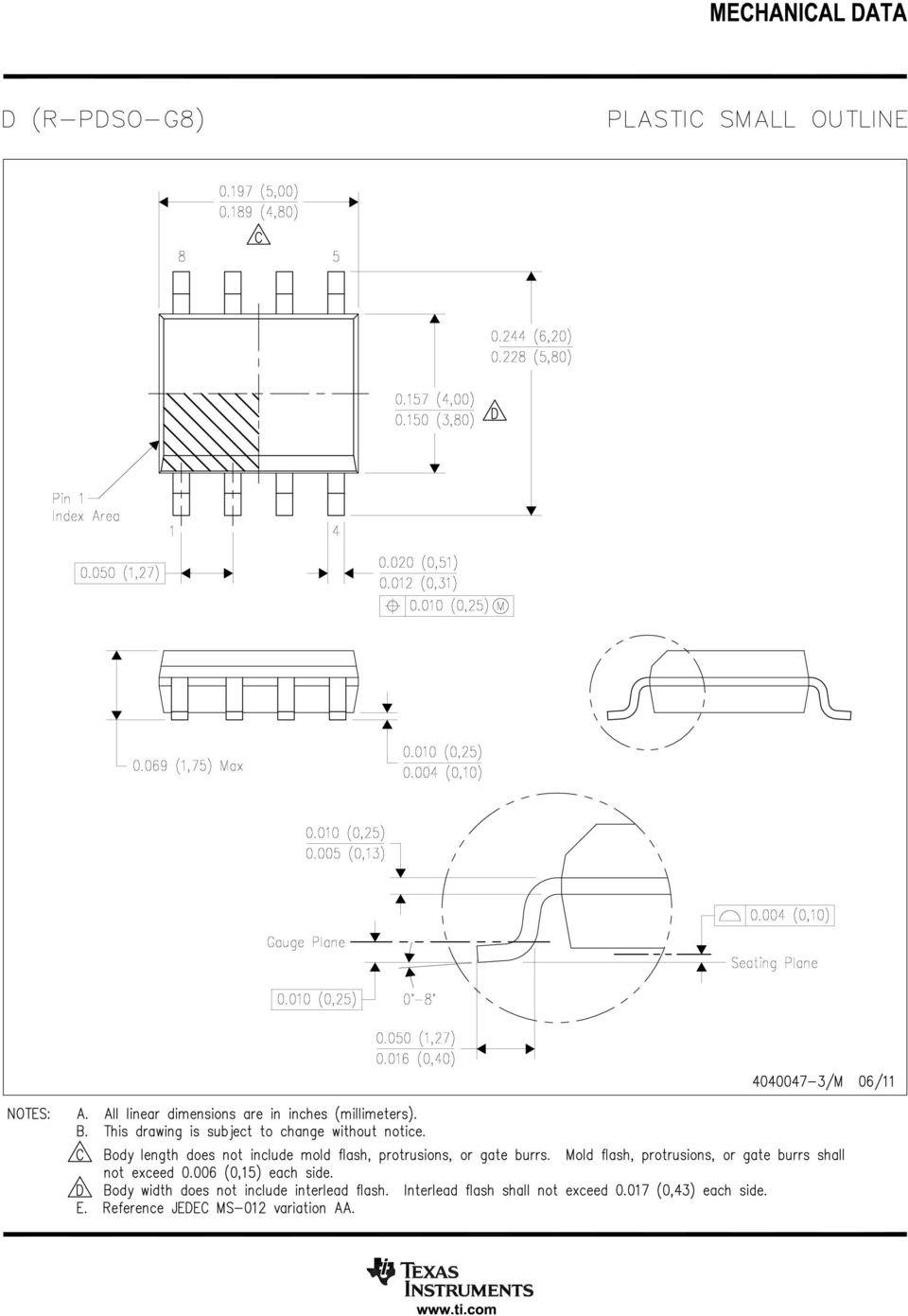
2 ABSOLUTE MAXIMUM RATINGS (1) Analog Input: Current... ±1mA, Momentary ±1mA, Continuous Voltage... GND.3V to V DD +.3V V DD to GND....3V to 6V V REF Voltage to GND....3V to V DD +.3V Digital Input Voltage to GND....3V to V DD +.3V Digital Output Voltage to GND....3V to V DD +.3V Lead Temperature (soldering, 1s) C Power Dissipation (any package)... 5mW NOTE: (1) Stresses above these ratings may cause permanent damage. Exposure to absolute maximum conditions for extended periods may degrade device reliability. ELECTROSTATIC DISCHARGE SENSITIVITY This integrated circuit can be damaged by ESD. Texas Instruments recommends that all integrated circuits be handled with appropriate precautions. Failure to observe proper handling and installation procedures can cause damage. ESD damage can range from subtle performance degradation to complete device failure. Precision integrated circuits may be more susceptible to damage because very small parametric changes could cause the device not to meet its published specifications. PACKAGE/ORDERING INFORMATION (1) SPECIFIED PACKAGE TEMPERATURE PACKAGE ORDERING TRANSPORT PRODUCT PACKAGE-LEAD DESIGNATOR RANGE MARKING NUMBER MEDIA, QUANTITY SO-8 D 4 C to +85 C U U Rails, 1 " " " " " U/2K5 Tape and Reel, 25 NOTE: (1) For the most current package and ordering information, see the Package Option Addendum at the end of this document, or see the TI web site at. PIN CONFIGURATION Top View +V IN 1 8 V REF V IN 2 7 GND U +V DD 3 6 SCLK CLK 4 5 DOUT/DRDY SO PIN DESCRIPTIONS PIN NAME PIN DESCRIPTION 1 +V IN Analog Input: Positive Input of the Differential Analog Input 2 V IN Analog Input: Negative Input of the Differential Analog Input 3 +V DD Input: Power-Supply Voltage, +5V 4 CLK Digital Input: Device System Clock. The system clock is in the form of a CMOScompatible clock. This is a Schmitt-Trigger input. 5 DOUT/DRDY Digital Output: Serial Data Output/Data Ready. A logic LOW on this output indicates that a new output word is available from the data output register. The serial data is clocked out of the serial data output shift register using SCLK. 6 SCLK Digital Input: Serial Clock. The serial clock is in the form of a CMOS-compatible clock. The serial clock operates independently from the system clock, therefore, it is possible to run SCLK at a higher frequency than CLK. The normal state of SCLK is LOW. Holding SCLK HIGH will either initiate a modulator reset for synchronizing multiple converters or enter power-down mode. This is a Schmitt-Trigger input. 7 GND Input: Ground 8 V REF Analog Input: Reference Voltage Input 2

3 ELECTRICAL CHARACTERISTICS All specifications at T MIN to T MAX, V DD = +5V, CLK = 16MHz, and V REF = 4.96V, unless otherwise specified. U PARAMETER CONDITIONS MIN TYP MAX UNITS ANALOG INPUT Full-Scale Input Voltage ±V REF V Absolute Input Voltage +V IN or V IN to GND.3 V DD V Differential Input Impedance CLK = 3.84kHz 125 MΩ CLK = 1MHz 48 kω CLK = 16MHz 3 kω Input Capacitance 2 pf Input Leakage At +25 C 5 5 pa At T MIN to T MAX 1 na DYNAMIC CHARACTERISTICS Data Rate 41.7 khz Bandwidth 3dB 9 khz Serial Clock (SCLK) 16 MHz System Clock Input (CLK) 16 MHz ACCURACY Integral Nonlinearity (1) ±.3 ±.15 % of FSR THD 1kHz Input;.1dB below FS 97 db Noise ppm of FSR, rms Resolution 24 Bits No Missing Codes 24 Bits Common-Mode Rejection (2) at DC 9 1 db Gain Error.4 1 % of FSR Offset Error ±1 ±2 ppm of FSR Gain Sensitivity to V REF V REF = 4.96V ±.1V 1:1 Power-Supply Rejection Ratio 6 8 db PERFORMANCE OVER TEMPERATURE Offset Drift.7 ppm/ C Gain Drift CLK = 16MHz 7.5 ppm/ C CLK = 14MHz 5.2 ppm/ C CLK = 12MHz 3.9 ppm/ C CLK < 1MHz 3.4 ppm/ C VOLTAGE REFERENCE V REF V DD V Load Current 22 µa DIGITAL INPUT/OUTPUT Logic Family CMOS Logic Level: V IH +4. +V DD +.3 V V IL V V OH I OH = 5µA +4.5 V V OL I OL = 5µA.4 V Input (SCLK, CLK) Hysteresis.6 V Data Format Offset Binary Two s Complement POWER-SUPPLY REQUIREMENTS Operation V Quiescent Current V DD = +5VDC 8 1 ma Operating Power 4 5 mw Power-Down Current 1 1 µa TEMPERATURE RANGE Operating C Storage 6 +1 C NOTES: (1) Applies to full-differential signals. (2) The common-mode rejection test is performed with a 1mV differential input. 3
 16 MHz System Clock Input (CLK) 16 MHz ACCURACY Integral Nonlinearity (1) ±.3 ±.15 % of FSR THD 1kHz Input;.1dB below FS 97 db Noise 2.5 3.")
4 TYPICAL CHARACTERISTICS At T A = +25 C, V DD = +5V, CLK = 16MHz, and V REF = 4.96V, unless otherwise specified. 3. RMS NOISE vs DATA OUTPUT RATE 19.5 EFFECTIVE RESOLUTION vs DATA OUTPUT RATE 2.5 RMS Noise (ppm of FS) Effective Resolution (bits) k 1k 1k k 1k 1k Data Output Rate (Hz) Data Output Rate (Hz) 3. RMS NOISE vs TEMPERATURE 19. EFFECTIVE RESOLUTION vs TEMPERATURE RMS Noise (ppm of FS) Effective Resolution (bits) Temperature ( C) Temperature ( C) 25 RMS NOISE vs V REF VOLTAGE 1 RMS NOISE vs V REF VOLTAGE 9 RMS Noise (µv) RMS Noise (ppm of FS) V REF (V) V REF (V) 4

5 TYPICAL CHARACTERISTICS (Cont.) At T A = +25 C, V DD = +5V, CLK = 16MHz, and V REF = 4.96V, unless otherwise specified. 3. RMS NOISE vs INPUT VOLTAGE 19. EFFECTIVE RESOLUTION vs V REF RMS Noise (ppm of FS) Effective Resolution (Bits) Differential Input Voltage (V) V REF (V) 4. INTEGRAL NON-LINEARITY vs TEMPERATURE 4 INTEGRAL NON-LINEARITY vs DATA OUTPUT RATE INL (ppm of FS) INL (ppm of FS) Temperature ( C) 1 1k 1k 1k Data Output Rate (Hz) Offset Drift (ppm of FS) OFFSET DRIFT vs TEMPERATURE GAIN DRIFT vs TEMPERATURE CLK = 16MHz CLK = 14.3MHz 2 2 CLK < 1MHz 4 CLK < 1MHz CLK = 16MHz Temperature ( C) Temperature ( C) Drift (ppm) 5
 2 1.")
6 TYPICAL CHARACTERISTICS (Cont.) At T A = +25 C, V DD = +5V, CLK = 16MHz, and V REF = 4.96V, unless otherwise specified. 1 POWER-SUPPLY REJECTION RATIO vs CLK FREQUENCY 11 COMMON-MODE REJECTION RATIO vs CLK FREQUENCY PSRR (db) CMRR (db) CLK Frequency (MHz) CLK Frequency (MHz) 9.5 CURRENT vs TEMPERATURE 45 POWER DISSIPATION vs CLOCK FREQUENCY 9. 4 Supply Current (ma) Power Dissipation (mw) Temperature ( C) CLK Frequency (MHz) TYPICAL FFT ANALYSIS OF THE 1kHz f S INPUT SIGNAL 2 Dynamic Range (db) Imput Signal Frequency (Hz) 6
 35 3 25 2 15 1 5.5 5 5.")
7 THEORY OF OPERATION The is a precision, high-dynamic range, 24-bit, deltasigma, A/D converter capable of achieving very high-resolution digital results at high data rates. The analog-input signal is sampled at a rate determined by the frequency of the system clock (CLK). The sampled analog input is modulated by the delta-sigma A/D modulator, which is followed by a digital filter. A Sinc 5 digital low-pass filter processes the output of the delta-sigma modulator and writes the result into the dataoutput register. The DOUT/DRDY pin is pulled LOW, indicating that new data is available to be read by the external microcontroller/microprocessor. As shown in the block diagram, the main functional blocks of the are the 4th-order delta-sigma modulator, a digital filter, control logic, and a serial interface. Each of these functional blocks is described below. ANALOG INPUT The contains a fully differential analog input. In order to provide low system noise, common-mode rejection of 1dB, and excellent power-supply rejection, the design topology is based on a fully differential switched-capacitor architecture. The bipolar input voltage range is from 4.96 to +4.96V, when the reference input voltage equals +4.96V; the bipolar range is with respect to V IN, and not with respect to GND. With regard to the analog input signal, the overall analog performance of the device is affected by three items. First, the input impedance can affect accuracy; therefore, if the source impedance of the input signal is significant, or if there is passive filtering prior to the, a significant portion of the signal can be lost across this external impedance. The magnitude of the effect is dependent on the desired system performance. See application note Understanding the ADS1251, ADS1253, and ADS1254 Input Circuitry (SBAA86), available for download from TI s web site,. Second, the current into or out of the analog inputs must be limited. Under no conditions should the current into or out of the analog inputs exceed 1mA. Third, to prevent aliasing of the input signal, the bandwidth of the analog input signal must be band limited; the bandwidth is a function of the system clock frequency. With a system clock frequency of 16MHz, the data-output rate is kHz with a 3dB frequency of 9kHz, where the 3dB frequency scales with the system clock frequency. To ensure the best linearity of the, a fully differential signal is recommended. BIPOLAR INPUT The differential inputs of the are designed to accept differential signals; however, each analog input voltage must stay between.3v and V DD. With a reference voltage at less than half of V DD, one input can be tied to the reference voltage, and the other input can range from V to 2 V REF. By using a single op amp circuit featuring a single amplifier and four external resistors, the can be configured to accept bipolar inputs referenced to ground. The conventional ±2.5V, ±5V, and ±1V input ranges can be interfaced to the using the resistor values shown in Figure 1. Bipolar Input 1kΩ 2kΩ R 2 BIPOLAR INPUT R1 R2 ±1V 2.5kΩ 5kΩ ±5V 5kΩ 1kΩ ±2.5V 1kΩ 2kΩ FIGURE 1. Level Shift Circuit for Bipolar Input Ranges. R 1 OPA235 REF 2.5V +IN IN OPA235 V REF 7

8 DELTA-SIGMA MODULATOR The operates from a nominal system clock frequency of 16MHz which is fixed in relation to the system clock frequency that is divided by 6 to derive the modulator frequency; therefore, with a system clock frequency of 16MHz, the modulator frequency is 2.667MHz. Furthermore, the oversampling ratio of the modulator is fixed in relation to the modulator frequency. The oversampling ratio of the modulator is 64, and with the modulator frequency running at 2.667MHz, the data rate is kHz; thus, using a slower system clock frequency will result in a lower data output rate, as shown in Table I. REFERENCE INPUT Reference input takes an average current of 22µA with a 16MHz system clock; this current will be proportional to the system clock. A buffered reference is recommended for. The recommended reference circuit is shown in Figure 2. Reference voltages higher than 4.96V will increase the fullscale range, whereas the absolute internal circuit noise of the converter remains the same. This will decrease the noise in terms of ppm of full scale, which increases the effective resolution (see the typical characteristic curve, RMS Noise vs V REF ). CLK (MHz) DATA OUTPUT RATE (Hz) DIGITAL FILTER 16. (1) (1) (1) (1) (1) (1) (1) (1) (1) (1) (1) (1) (1) (1) (1) (1) (1) The digital filter of the, referred to as a sinc 5 filter, computes the digital result based on the most recent outputs from the delta-sigma modulator. At the most basic level, the digital filter can be thought of as simply averaging the modulator results in a weighted form and presenting this average as the digital output. The digital output rate, or data rate, scales directly with the system CLK frequency, this allows the data output rate to be changed over a very wide range (five orders of magnitude) by changing the system CLK frequency. However, it is important to note that the 3dB point of the filter is.216 times the data output rate, so the data output rate must allow for sufficient margin to prevent attenuation of the signal of interest. As the conversion result is essentially an average, the data-output rate determines the location of the resulting notches in the digital filter (see Figure 3). Note that the first notch is located at the data-output rate frequency, and subsequent notches are located at integer multiples of the data-output rate to allow for rejection of not only the fundamental frequency, but also harmonic frequencies. In this manner, the data-output rate can be used to set specific notch frequencies in the digital filter response. NOTE: (1) Standard Clock Oscillator. TABLE I. CLK Rate versus Data Output Rate. +5V +5V.1µF.1µF REF µF 1kΩ + 1µF.1µF 3 OPA µF.1µF To V REF Pin 8 of the FIGURE 2. Recommended External Voltage Reference Circuit for Best Low-Noise Operation with the. 8

9 For example, if the rejection of power-line frequencies is desired, then the data-output rate can simply be set to the power-line frequency. For 5Hz rejection, the system CLK frequency must be 19.2kHz, and this will set the dataoutput rate to 5Hz (see Table I and Figure 4). For 6Hz rejection, the system CLK frequency must be 2.4kHz, and this will set the data-output rate to 6Hz (see Table I and Figure 5). If both 5Hz and 6Hz rejection is required, then the system CLK must be 3.84kHz; this will set the dataoutput rate to 1Hz and reject both 5Hz and 6Hz (see Table I and Figure 6). There is an additional benefit in using a lower data-output rate: it provides better rejection of signals in the frequency band of interest. For example, with a 5Hz data-output rate, a significant signal at 75Hz can alias back into the passband at 25Hz; this is due to the fact that rejection at 75Hz must only be 66dB in the stopband frequencies higher than the first-notch frequency (see Figure 4). However, setting the data-output rate to 1Hz will provide 135dB rejection at 75Hz (see Figure 6). A similar benefit is gained at frequencies near the data-output rate (see Figures 7, 8, 9, and 1). For example, with a 5Hz data-output rate, rejection at 55Hz may only be 15dB (see Figure 7); however, with a 1Hz dataoutput rate, rejection at 55Hz will be 122dB (see Figure 8). If a slower data-output rate does not meet the system requirements, then the analog front end can be designed to provide the needed attenuation to prevent aliasing. Additionally, the data-output rate can be increased and additional digital filtering can be done in the processor or controller. Application note SBAA13, A Spreadsheet to Calculate the Frequency Response of the ADS (available for download at ) provides a simple tool for calculating the ADS125 frequency response for any CLK frequency. The digital filter is described by the following transfer function: Hf () = 5 π f 64 sin f MOD π f 64 sin f MOD or 5 64 z Hz ( ) = ( 1 z ) The digital filter requires five conversions to fully settle. The modulator has an oversampling ratio of 64; therefore, it requires 5 64, or 32 modulator results, or clocks, to fully settle. As the modulator clock is derived from the system clock (CLK) (modulator clock = CLK 6), the number of system clocks required for the digital filter to fully settle is , or 192 CLKs. This means that any significant step change at the analog input requires five full conversions to settle. However, if the analog input change occurs asynchronously to the DOUT/DRDY pulse, then six conversions are required to ensure full settling. CONTROL LOGIC The control logic is used for communications and control of the. Power-Up Sequence Prior to power-up, all digital and analog-input pins must be LOW. At the time of power-up, these signal inputs can be biased to a voltage other than V, however, they must never exceed +V DD. Once the powers up, the DOUT/DRDY line pulses LOW on the first conversion; this data is not valid. The sixth pulse of DOUT/DRDY is valid data from the analog input signal. DOUT/DRDY The DOUT/DRDY output signal alternates between two modes of operation. The first mode of operation is the Data Ready (DRDY) mode to indicate that new data has been loaded into the data-output register and is ready to be read. The second mode of operation is the Data Output (DOUT) mode and is used to serially shift data out of the Data Output Register (DOR). See Figure 11 for the time domain partitioning of the DRDY and DOUT function. See Figure 12 for the basic timing of DOUT/DRDY. During the time defined by t 2, t 3, and t 4, the DOUT/DRDY pin functions in DRDY mode. The state of the DOUT/DRDY pin is HIGH prior to the internal transfer of new data to the DOR. The result of the A/D conversion is written 9
.")
10 NORMALIZED DIGITAL FILTER RESPONSE DIGITAL FILTER RESPONSE Gain (db) Gain (db) Frequency (Hz) Frequency (Hz) FIGURE 3. Normalized Digital Filter Response. FIGURE 4. Digital Filter Response (5Hz). DIGITAL FILTER RESPONSE DIGITAL FILTER RESPONSE Gain (db) Gain (db) Frequency (Hz) Frequency (Hz) FIGURE 5. Digital Filter Response (6Hz). FIGURE 6. Digital Filter Response (1Hz Multiples). DIGITAL FILTER RESPONSE DIGITAL FILTER RESPONSE Gain (db) Gain (db) Frequency (Hz) Frequency (Hz) FIGURE 7. Expanded Digital Filter Response (5Hz with a 5Hz Notch). FIGURE 8. Expanded Digital Filter Response (5Hz with a 1Hz Notch). 1
. FIGURE 6. Digital Filter Response (1Hz Multiples).")
11 Gain (db) DIGITAL FILTER RESPONSE Frequency (Hz) to the DOR from MSB to LSB in the time defined by t 1 (see Figures 11 and 12). The DOUT/DRDY line then drives the line LOW for the time defined by t 2, and then drives the line HIGH for the time defined by t 3 to indicate that new data is available to be read. At this point, the function of the DOUT/ DRDY pin changes to DOUT mode, and data is shifted out on the pin after t 7. If the MSB is high (because of a negative result) the DOUT/DRDY signal will stay HIGH after the end of time t 3. The device communicating with the can provide SCLKs to the after the time defined by t 6. The normal mode of reading data from the is for the device reading the to latch the data on the rising edge of SCLK (since data is shifted out of the on the falling edge of SCLK). In order to retrieve valid data, the entire DOR must be read before the DOUT/DRDY pin reverts back to DRDY mode. FIGURE 9. Expanded Digital Filter Response (6Hz with a 6Hz Notch). Gain (db) DIGITAL FILTER RESPONSE Frequency (Hz) FIGURE 1. Expanded Digital Filter Response (6Hz with a 1Hz Notch). If SCLKs are not provided to the during the DOUT mode, the MSB of the DOR is present on the DOUT/DRDY line until the beginning of the time defined by t 4. If an incomplete read of the takes place in DOUT mode (that is, fewer than 24 SCLKs are provided), the state of the last bit read is present on the DOUT/DRDY line until the beginning of the time defined by t 4. If more than 24 SCLKs are provided during DOUT mode, the DOUT/DRDY line stays LOW until the beginning of the time defined by t 4. The internal data pointer for shifting data out on DOUT/DRDY is reset on the falling edge of the time defined by t 1 and t 4. This ensures that the first bit of data shifted out of the after DRDY mode is always the MSB of new data. SYNCHRONIZING MULTIPLE CONVERTERS The normal state of SCLK is LOW; however, by holding SCLK HIGH, multiple s can be synchronized. This is accomplished by holding SCLK HIGH for at least four, but less than 2, consecutive DOUT/DRDY cycles (see Figure 13). After the circuitry detects that SCLK has been held HIGH for four consecutive DOUT/DRDY cycles, the DOUT/ DRDY pin pulses LOW for 3 CLK cycles and then held HIGH, and the modulator is held in a reset state. The modulator is released from reset and synchronization occurs on the falling edge of SCLK. It is important to note that prior to synchronization, the DOUT/DRDY pulse of multiple s in the system can have a difference in timing up to one DRDY period. Therefore, to ensure synchronization, the SCLK must be held HIGH for at least five DRDY cycles. The first DOUT/DRDY pulse after the falling edge of SCLK occurs at t 14. Valid data is not present until the sixth DOUT/DRDY pulse. 11
 the DOUT/DRDY signal will stay HIGH after the end of time t 3.")
12 POWER-DOWN MODE The normal state of SCLK is LOW; however, by holding SCLK HIGH, the enters power-down mode. This is accomplished by holding SCLK HIGH for at least 2 consecutive DOUT/DRDY periods (see Figure 14). After the circuitry detects that SCLK is held HIGH for four consecutive DOUT/DRDY cycles, the DOUT/DRDY pin pulses LOW for three CLK cycles, then held HIGH, and the modulator will be held in a reset state. If SCLK is held HIGH for an additional 16 DOUT/DRDY periods, the enters power-down mode and the part is released from power-down mode on the falling edge of SCLK. It is important to note that the DOUT/DRDY pin is held HIGH after four DOUT/DRDY cycles, but power-down mode is not entered for an additional 16 DOUT/DRDY periods. The first DOUT/DRDY pulse after the falling edge of SCLK occurs at t 16 ; however, subsequent DOUT/DRDY pulses occur normally. Valid data is not present until the sixth DOUT/DRDY pulse. SERIAL INTERFACE The includes a simple serial interface which can be connected to microcontrollers and digital signal processors in a variety of ways. Communications with the can commence on the first detection of the DOUT/DRDY pulse after power up, although data is valid until the sixth conversion. It is important to note that the data from the is a 24-bit result transmitted MSB-first in Offset Binary Two s Complement format, as shown in Table III. The data must be clocked out before the enters DRDY mode to ensure reception of valid data, as described in the DOUT/DRDY section of this data sheet. DIFFERENTIAL VOLTAGE INPUT +Full-Scale Zero Full-Scale DIGITAL OUTPUT (HEX) 7FFFFF H H 8 H TABLE III. Data Format (Offset Binary Two's Complement). SYMBOL DESCRIPTION MIN TYP MAX UNITS t DRDY Conversion Cycle 384 CLK ns DRDY Mode DRDY Mode 36 CLK ns DOUT Mode DOUT Mode 348 CLK ns t 1 DOR Write Time 6 CLK ns t 2 DOUT/DRDY LOW Time 6 CLK ns t 3 DOUT/DRDY HIGH Time (Prior to Data Out) 6 CLK ns t 4 DOUT/DRDY HIGH Time (Prior to Data Ready) 24 CLK ns t 5 Rising Edge of CLK to Falling Edge of DOUT/DRDY 3 ns t 6 End of DRDY Mode to Rising Edge of First SCLK 3 ns t 7 End of DRDY Mode to Data Valid (Propagation Delay) 3 ns t 8 Falling Edge of SCLK to Data Valid (Hold Time) 5 ns t 9 Falling Edge of SCLK to Next Data Out Valid (Propagation Delay) 3 ns t 1 SCLK Setup Time for Synchronization or Power Down 3 ns t 11 DOUT/DRDY Pulse for Synchronization or Power Down 3 CLK ns t 12 Rising Edge of SCLK Until Start of Synchronization 1537 CLK 7679 CLK ns t 13 Synchronization Time.5 CLK CLK ns t 14 Falling Edge of CLK (After SCLK Goes LOW) Until Start of DRDY Mode CLK ns t 15 Rising Edge of SCLK Until Start of Power Down 7681 CLK ns t 16 Falling Edge of CLK (After SCLK Goes LOW) Until Start of DRDY Mode CLK CLK ns t 17 Falling Edge of Last DOUT/DRDY to Start of Power Down CLK ns TABLE II. Digital Timing. DOUT Mode DRDY Mode DOUT Mode DRDY Mode t 4 t 2 t 3 DOUT/DRDY DATA DATA DATA t 1 FIGURE 11. DOUT/DRDY Partitioning. 12

13 CLK t 5 t 6 SCLK t 1 t 7 t 8 t 9 DOUT/DRDY MSB LSB t 4 t 2 t 3 DRDY Mode DOUT Mode t DRDY FIGURE 12. DOUT/DRDY Timing. Synchronization Mode Starts Here CLK t 1 Synchronization Begins Here SCLK t 12 DOUT/DRDY DATA DATA DATA DOUT Mode t 2 t 3 t 4 t 11 t DRDY 4 t DRDY t 3 t 4 t 2 DOUT t 13 t 14 t DRDY Mode FIGURE 13. Synchronization Mode. Power Down Occurs Here CLK t 1 t 17 SCLK t 15 DOUT/DRDY DATA DATA DATA DOUT Mode t 2 t 3 t 4 t 11 t 11 t DRDY 4 t DRDY t 3 t 4 t 2 DOUT t 16 t DRDY Mode FIGURE 14. Power-Down Mode. 13

14 ISOLATION The serial interface of the provides for simple isolation methods. The CLK signal can be local to the, which then only requires two signals (SCLK and DOUT/DRDY) to be used for isolated data acquisition. LAYOUT POWER SUPPLY The power supply should be well regulated and low noise. For designs requiring very high resolution from the, power-supply rejection will be a concern. Avoid running digital lines under the device because they can couple noise onto the die. High-frequency noise can capacitively couple into the analog portion of the device and will alias back into the passband of the digital filter, affecting the conversion result. GROUNDING The analog and digital sections of the system design must be carefully and cleanly partitionedl; each section must have its own ground plane with no overlap between them. GND must be connected to the analog ground plane, as well as all other analog grounds. Do not join the analog and digital ground planes on the board, but instead connect the two with a moderate signal trace. For multiple converters, connect the two ground planes at one location as central to all of the converters as possible. In some cases, experimentation is required to find the best point to connect the two planes together. The printed circuit board can be designed to provide different analog/digital ground connections via short jumpers; the initial prototype can be used to establish which connection works best. DECOUPLING Good decoupling practices must be used for the and for all components in the design. All decoupling capacitors, and specifically the.1µf ceramic capacitors, must be placed as close as possible to the pin being decoupled. A 1µF to 1µF capacitor, in parallel with a.1µf ceramic capacitor, must be used to decouple V DD to GND. SYSTEM CONSIDERATIONS The recommendations for power supplies and grounding change depending on the requirements and specific design of the overall system. Achieving 24 bits of noise performance is a great deal more difficult than achieving 12 bits of noise performance. In general, a system can be broken up into four different stages: Analog Processing Analog Portion of the Digital Portion of the Digital Processing For the simplest system consisting of minimal analog signal processing (basic filtering and gain), a microcontroller, and one clock source, one can achieve high resolution by powering all components by a common power supply. In addition, all components can share a common ground plane; thus, there would be no distinctions between analog power and ground, and digital power and ground. The layout must still include a power plane, a ground plane, and careful decoupling. In a more extreme case, the design can include: Multiple s Extensive Analog Signal Processing One or More Microcontrollers, Digital Signal Processors, or Microprocessors Many Different Clock Sources Interconnections to Various Other Systems High resolution will be very difficult to achieve for this design. The approach would be to break the system into as many different parts as possible. For example, each may have its own analog processing front end. DEFINITION OF TERMS An attempt has been made to be consistent with the terminology used in this data sheet. In that regard, the definition of each term is given as follows: Analog-Input Differential Voltage for an analog signal that is fully differential, the voltage range can be compared to that of an instrumentation amplifier. For example, if both analog inputs of the are at 2.48V, the differential voltage is V; however, if one analog input is at V and the other analog input is at 4.96V, then the differential voltage magnitude is 4.96V. This is the case regardless of which input is at V and which is at 4.96V. The digital-output 14

15 result, however, is quite different. The analog-input differential voltage is given by the following equation: +V IN ( V IN ) A positive digital output is produced whenever the analog-input differential voltage is positive, whereas negative digital output is produced whenever the differential is negative. For example, a positive full-scale output is produced when the converter is configured with a 4.96V reference, and the analog-input differential is 4.96V, the negative fullscale output is produced when the differential voltage is 4.96V. In each case, the actual input voltages must remain within the.3v to +V DD range. Actual Analog-Input Voltage the voltage at any one analog input relative to GND. Full-Scale Range (FSR) as with most A/D converters, the full-scale range of the is defined as the input which produces the positive full-scale digital output minus the input which produces the negative full-scale digital output. For example, when the converter is configured with a 4.96V reference, the differential full-scale range is: [4.96V (positive full-scale) ( 4.96V) (negative full-scale)] = 8.192V Least Significant Bit (LSB) Weight this is the theoretical amount of voltage that the differential voltage at the analog input has to change in order to observe a change in the output data of one least significant bit. It is computed as follows: Full ScaleRange LSB Weight = N 2 where N is the number of bits in the digital output. Conversion Cycle as used here, a conversion cycle refers to the time period between DOUT/DRDY pulses. Effective Resolution (ER) of the in a particular configuration can be expressed in two different units: bits rms (referenced to output) and µvrms (referenced to input). Computed directly from the converter output data, each is a statistical calculation based on a given number of results. Noise occurs randomly; the rms value represents a statistical measure which is one standard deviation. The ER in bits can be computed as follows: 2 VREF 2 log Vrms noise ER in bits rms = 62. The 2 V REF figure in each calculation represents the full-scale range of the, this means that both units are absolute expressions of resolution the performance in different configurations can be directly compared, regardless of the units. Noise Reduction for random noise, the ER can be improved with averaging. The result is the reduction in noise by the factor N, where N is the number of averages, as shown in Table IV; this can be used to achieve true 24-bit performance at a lower data rate. To achieve 24 bits of resolution, more than 24 bits must be accumulated. A 36-bit accumulator is required to achieve an ER of 24 bits. The following uses V REF = 4.96V, with the outputting data at 4kHz, a 496 point average takes 12.4ms. The benefits of averaging is degraded if the input signal drifts during that 1ms. N NOISE ER ER (NUMBER REDUCTION IN IN OF AVERAGES) FACTOR µvrms BITS rms µV µV µV µV µV µV µV µV µV µV nV nV nV 24 TABLE IV. Averaging. 15

16 Revision History DATE REVISION PAGE SECTION DESCRIPTION 6/6 D 11 DOUT/DRDY Text changes to DOUT/DRDY section. NOTE: Page numbers for previous revisions may differ from page numbers in the current version. 16

17 PACKAGE OPTION ADDENDUM 3-Jun-216 PACKAGING INFORMATION Orderable Device Status (1) Package Type Package Drawing Pins Package Qty Eco Plan U ACTIVE SOIC D 8 75 Green (RoHS & no Sb/Br) U/2K5 ACTIVE SOIC D 8 25 Green (RoHS & no Sb/Br) U/2K5G4 ACTIVE SOIC D 8 25 Green (RoHS & no Sb/Br) UG4 ACTIVE SOIC D 8 75 Green (RoHS & no Sb/Br) (2) Lead/Ball Finish (6) MSL Peak Temp (3) Op Temp ( C) CU NIPDAU Level-2-26C-1 YEAR -4 to 85 ADS 1252U CU NIPDAU Level-2-26C-1 YEAR -4 to 85 ADS 1252U CU NIPDAU Level-2-26C-1 YEAR -4 to 85 ADS 1252U CU NIPDAU Level-2-26C-1 YEAR -4 to 85 ADS 1252U Device Marking (4/5) Samples (1) The marketing status values are defined as follows: ACTIVE: Product device recommended for new designs. LIFEBUY: TI has announced that the device will be discontinued, and a lifetime-buy period is in effect. NRND: Not recommended for new designs. Device is in production to support existing customers, but TI does not recommend using this part in a new design. PREVIEW: Device has been announced but is not in production. Samples may or may not be available. OBSOLETE: TI has discontinued the production of the device. (2) Eco Plan - The planned eco-friendly classification: Pb-Free (RoHS), Pb-Free (RoHS Exempt), or Green (RoHS & no Sb/Br) - please check for the latest availability information and additional product content details. TBD: The Pb-Free/Green conversion plan has not been defined. Pb-Free (RoHS): TI's terms "Lead-Free" or "Pb-Free" mean semiconductor products that are compatible with the current RoHS requirements for all 6 substances, including the requirement that lead not exceed.1% by weight in homogeneous materials. Where designed to be soldered at high temperatures, TI Pb-Free products are suitable for use in specified lead-free processes. Pb-Free (RoHS Exempt): This component has a RoHS exemption for either 1) lead-based flip-chip solder bumps used between the die and package, or 2) lead-based die adhesive used between the die and leadframe. The component is otherwise considered Pb-Free (RoHS compatible) as defined above. Green (RoHS & no Sb/Br): TI defines "Green" to mean Pb-Free (RoHS compatible), and free of Bromine (Br) and Antimony (Sb) based flame retardants (Br or Sb do not exceed.1% by weight in homogeneous material) (3) MSL, Peak Temp. - The Moisture Sensitivity Level rating according to the JEDEC industry standard classifications, and peak solder temperature. (4) There may be additional marking, which relates to the logo, the lot trace code information, or the environmental category on the device. (5) Multiple Device Markings will be inside parentheses. Only one Device Marking contained in parentheses and separated by a "~" will appear on a device. If a line is indented then it is a continuation of the previous line and the two combined represent the entire Device Marking for that device. (6) Lead/Ball Finish - Orderable Devices may have multiple material finish options. Finish options are separated by a vertical ruled line. Lead/Ball Finish values may wrap to two lines if the finish value exceeds the maximum column width. Addendum-Page 1
 Samples (1) The marketing status values are defined as follows: ACTIVE: Product device recommended for new designs.")
18 PACKAGE OPTION ADDENDUM 3-Jun-216 Important Information and Disclaimer:The information provided on this page represents TI's knowledge and belief as of the date that it is provided. TI bases its knowledge and belief on information provided by third parties, and makes no representation or warranty as to the accuracy of such information. Efforts are underway to better integrate information from third parties. TI has taken and continues to take reasonable steps to provide representative and accurate information but may not have conducted destructive testing or chemical analysis on incoming materials and chemicals. TI and TI suppliers consider certain information to be proprietary, and thus CAS numbers and other limited information may not be available for release. In no event shall TI's liability arising out of such information exceed the total purchase price of the TI part(s) at issue in this document sold by TI to Customer on an annual basis. Addendum-Page 2

19
20

21 IMPORTANT NOTICE Texas Instruments Incorporated and its subsidiaries (TI) reserve the right to make corrections, enhancements, improvements and other changes to its semiconductor products and services per JESD46, latest issue, and to discontinue any product or service per JESD48, latest issue. Buyers should obtain the latest relevant information before placing orders and should verify that such information is current and complete. All semiconductor products (also referred to herein as components ) are sold subject to TI s terms and conditions of sale supplied at the time of order acknowledgment. TI warrants performance of its components to the specifications applicable at the time of sale, in accordance with the warranty in TI s terms and conditions of sale of semiconductor products. Testing and other quality control techniques are used to the extent TI deems necessary to support this warranty. Except where mandated by applicable law, testing of all parameters of each component is not necessarily performed. TI assumes no liability for applications assistance or the design of Buyers products. Buyers are responsible for their products and applications using TI components. To minimize the risks associated with Buyers products and applications, Buyers should provide adequate design and operating safeguards. TI does not warrant or represent that any license, either express or implied, is granted under any patent right, copyright, mask work right, or other intellectual property right relating to any combination, machine, or process in which TI components or services are used. Information published by TI regarding third-party products or services does not constitute a license to use such products or services or a warranty or endorsement thereof. Use of such information may require a license from a third party under the patents or other intellectual property of the third party, or a license from TI under the patents or other intellectual property of TI. Reproduction of significant portions of TI information in TI data books or data sheets is permissible only if reproduction is without alteration and is accompanied by all associated warranties, conditions, limitations, and notices. TI is not responsible or liable for such altered documentation. Information of third parties may be subject to additional restrictions. Resale of TI components or services with statements different from or beyond the parameters stated by TI for that component or service voids all express and any implied warranties for the associated TI component or service and is an unfair and deceptive business practice. TI is not responsible or liable for any such statements. Buyer acknowledges and agrees that it is solely responsible for compliance with all legal, regulatory and safety-related requirements concerning its products, and any use of TI components in its applications, notwithstanding any applications-related information or support that may be provided by TI. Buyer represents and agrees that it has all the necessary expertise to create and implement safeguards which anticipate dangerous consequences of failures, monitor failures and their consequences, lessen the likelihood of failures that might cause harm and take appropriate remedial actions. Buyer will fully indemnify TI and its representatives against any damages arising out of the use of any TI components in safety-critical applications. In some cases, TI components may be promoted specifically to facilitate safety-related applications. With such components, TI s goal is to help enable customers to design and create their own end-product solutions that meet applicable functional safety standards and requirements. Nonetheless, such components are subject to these terms. No TI components are authorized for use in FDA Class III (or similar life-critical medical equipment) unless authorized officers of the parties have executed a special agreement specifically governing such use. Only those TI components which TI has specifically designated as military grade or enhanced plastic are designed and intended for use in military/aerospace applications or environments. Buyer acknowledges and agrees that any military or aerospace use of TI components which have not been so designated is solely at the Buyer's risk, and that Buyer is solely responsible for compliance with all legal and regulatory requirements in connection with such use. TI has specifically designated certain components as meeting ISO/TS16949 requirements, mainly for automotive use. In any case of use of non-designated products, TI will not be responsible for any failure to meet ISO/TS Products Applications Audio /audio Automotive and Transportation /automotive Amplifiers amplifier.ti.com Communications and Telecom /communications Data Converters dataconverter.ti.com Computers and Peripherals /computers DLP Products Consumer Electronics /consumer-apps DSP dsp.ti.com Energy and Lighting /energy Clocks and Timers /clocks Industrial /industrial Interface interface.ti.com Medical /medical Logic logic.ti.com Security /security Power Mgmt power.ti.com Space, Avionics and Defense /space-avionics-defense Microcontrollers microcontroller.ti.com Video and Imaging /video RFID OMAP Applications Processors /omap TI E2E Community e2e.ti.com Wireless Connectivity /wirelessconnectivity Mailing Address: Texas Instruments, Post Office Box 65533, Dallas, Texas Copyright 216, Texas Instruments Incorporated
24-Bit, 20kHz, Low-Power ANALOG-TO-DIGITAL CONVERTER
 ADS1251 ADS1251 MARCH 21 REVISED JUNE 29 24-Bit, 2kHz, Low-Power ANALOG-TO-DIGITAL CONVERTER FEATURES 24 BITS NO MISSING CODES 19 BITS EFFECTIVE RESOLUTION UP TO 2kHz DATA RATE LOW NOISE: 1.5ppm DIFFERENTIAL
Data sheet acquired from Harris Semiconductor SCHS078C -- Revised October 2003
 Data sheet acquired from Harris Semiconductor SCHS078C -- Revised October 2003 The CD4521B types are supplied in 16-lead dual-in-line plastic packages (E suffix), 16-lead small-outline packages (M, M96,
SDLS940A MARCH 1974 REVISED MARCH 1988. Copyright 1988, Texas Instruments Incorporated
 SN5490A, SN5492A, SN5493A, SN54LS90, SN54LS92, SN54LS93 SN7490A, SN7492A, SN7493A, SN74LS90, SN74LS92, SN74LS93 DECADE, DIVIDE-BY-TWELVE AND BINARY COUNTERS SDLS940A MARCH 1974 REVISED MARCH 1988 PRODUCTION
FEATURES APPLICATIONS
 FEATURES DIGITALLY-CONTROLLED ANALOG VOLUME CONTROL: Four Independent Audio Channels Serial Control Interface Zero Crossing Detection Mute Function WIDE GAIN AND ATTENUATION RANGE: +31.5dB to 95.5dB with
with Ultra-Fast Transient Response and High Light-Load Efficiency
 1 Adaptor 6-24V Optional N-FET Driver Ultra-Fast DPM Simplified Application Diagram Iin Ultra-Low Quiescent Current Enhanced Safety Features OCP, OVP, FET Short Support CPU Turbo Mode To System bq24715
Data sheet acquired from Harris Semiconductor SCHS020C Revised October 2003
 Data sheet acquired from Harris Semiconductor SCHS020C Revised October 2003 The CD4009UB and CD4010B types are supplied in 16-lead hermetic dual-in-line ceramic packages (F3A suffix), 16-lead dual-in-line
Data sheet acquired from Harris Semiconductor SCHS067B Revised July 2003
 Data sheet acquired from Harris Semiconductor SCHS067B Revised July 2003 The CD4502B types are supplied in 16-lead hermetic dual-in-line ceramic packages (F3A suffix), 16-lead dual-in-line plastic packages
AMC1100: Replacement of Input Main Sensing Transformer in Inverters with Isolated Amplifier
 Application Report SLAA552 August 2012 AMC1100: Replacement of Input Main Sensing Transformer in Inverters with Isolated Amplifier Ambreesh Tripathi and Harmeet Singh Analog/Digital Converters ABSTRACT
 PACKAGE OPTION ADDENDUM www.ti.com 12-Jan-2006 PACKAGING INFORMATION Orderable Device Status (1) Package Type Package Drawing Pins Package Qty Eco Plan (2) Lead/Ball Finish MSL Peak Temp (3) 76005012A
LM556 LM556 Dual Timer
 LM556 LM556 Dual Timer Literature Number: SNAS549 LM556 Dual Timer General Description The LM556 Dual timing circuit is a highly stable controller capable of producing accurate time delays or oscillation.
Data sheet acquired from Harris Semiconductor SCHS087D Revised October 2003
 Data sheet acquired from Harris Semiconductor SCHS087D Revised October 2003 The CD4555B and CD4556B types are supplied in 16-lead hermetic dual-in-line ceramic packages (F3A suffix), 16-lead dual-in-line
CD4071B Quad 2-Input OR Gate CD4072B Dual 4-Input OR Gate CD4075B Triple 3-Input OR Gate
 Data sheet acquired from Harris Semiconductor SCHS056D Revised August 2003 CD4071B Quad 2-Input OR Gate CD4072B Dual 4-Input OR Gate CD4075B Triple 3-Input OR Gate CD4071B, CD4072B, and CD4075B OR gates
Data sheet acquired from Harris Semiconductor SCHS049C Revised October 2003
 Data sheet acquired from Harris Semiconductor SCHS049C Revised October 2003 CD4060B consists of an oscillator section and 14 ripple-carry binary counter stages. The oscillator configuration allows design
16-Bit, 10µs Sampling, CMOS ANALOG-to-DIGITAL CONVERTER
 JANUARY 1996 REVISED OCTOBER 2006 16-Bit, 10µs Sampling, CMOS ANALOG-to-DIGITAL CONVERTER FEATURES 100kHz min SAMPLING RATE STANDARD ±10V INPUT RANGE 86dB min SINAD WITH 20kHz INPUT ±3.0 LSB max INL DNL:
 PACKAGE OPTION ADDENDUM www.ti.com 12-Jan-2006 PACKAGING INFORMATION Orderable Device Status (1) Package Type Package Drawing Pins Package Qty Eco Plan (2) Lead/Ball Finish MSL Peak Temp (3) 5962-9557401QCA
24-Bit ANALOG-TO-DIGITAL CONVERTER
 ADS1211 ADS1211 ADS1211 ADS1210 ADS1210 ADS1210 ADS1211 JANUARY 1996 REVISED SEPTEMBER 2005 24-Bit ANALOG-TO-DIGITAL CONVERTER FEATURES DELTA-SIGMA A/D CONVERTER 23 BITS EFFECTIVE RESOLUTION AT 10Hz AND
RF37S114 Tag-it HF-I Type 5 NFC, ISO/IEC 15693 Transponder, 4 mm 4 mm
 1 1 Product Folder Sample & Buy Technical Documents Tools & Software Support & Community RF37S114 SCBS907 NOVEMBER 2015 RF37S114 Tag-it HF-I Type 5 NFC, ISO/IEC 15693 Transponder, 4 mm 4 mm 1 Device Overview
Application Note AN107
 Murata Balun for CC253x and CC254x LFB182G45BG2D280 By Fredrik Kervel Keywords Balun LFB182G45BG2D280 CC253x CC254x CC257x CC85xx 1 Introduction Murata s LFB182G45BG2D280 integrated balun is specially
LM5030 LM5030 Application: DC - DC Converter Utilizing the Push-Pull Topology
 LM5030 LM5030 Application: DC - DC Converter Utilizing the Push-Pull Topology Literature Number: SNVA553 LM5030 Application DC DC Converter Utilizing the Push-Pull Topology 1 Push-Pull Topology D1 L +
16-Bit DIGITAL-TO-ANALOG CONVERTER With Serial Data Interface
 SBAS0A JULY 997 REVISED NOVEMBER 00 -Bit DIGITAL-TO-ANALOG CONVERTER With Serial Data Interface FEATURES: SERIAL DIGITAL INTERFACE VOLTAGE OUTPUT: ±0V, ±V, 0 to +0V ± LSB INTEGRAL LINEARITY -BIT MONOTONIC
3V Video Amplifier with 6dB Gain and Filter in SC70
 OPA360 SB0S294E DECEMBER 2003 REVISED SEPTEMBER 2006 3V Video Amplifier with 6dB Gain and Filter in SC70 FEATURES EXCELLENT VIDEO PERFORMANCE INTERNAL GAIN: 6dB 2-POLE RECONSTRUCTION FILTER SAG CORRECTION
Stereo Audio Volume Control
 PGA2320 Stereo Audio Volume Control FEATURES DIGITALLY-CONTROLLED ANALOG VOLUME CONTROL: Two Independent Audio Channels Serial Control Interface Zero Crossing Detection Mute Function WIDE GAIN AND ATTENUATION
Wireless Subwoofer TI Design Tests
 Wireless Subwoofer TI Design Tests This system design was tested for THD+N vs. frequency at 5 watts and 30 watts and THD+N vs. power at 00. Both the direct analog input and the wireless systems were tested.
Wide Bandwidth, Fast Settling Difet OPERATIONAL AMPLIFIER
 Wide Bandwidth, Fast Settling Difet OPERATIONAL AMPLIFIER FEATURES HIGH GAIN-BANDWIDTH: 35MHz LOW INPUT NOISE: 1nV/ Hz HIGH SLEW RATE: V/µs FAST SETTLING: 24ns to.1% FET INPUT: I B = 5pA max HIGH OUTPUT
Cold-Junction-Compensated K-Thermocoupleto-Digital Converter (0 C to +1024 C)
") 19-2235; Rev 1; 3/02 Cold-Junction-Compensated K-Thermocoupleto-Digital General Description The performs cold-junction compensation and digitizes the signal from a type-k thermocouple. The data is output
19-2235; Rev 1; 3/02 Cold-Junction-Compensated K-Thermocoupleto-Digital General Description The performs cold-junction compensation and digitizes the signal from a type-k thermocouple. The data is output
54LS174,54LS175,DM54LS174,DM54LS175, DM74LS174,DM74LS175
 54LS174,54LS175,DM54LS174,DM54LS175, DM74LS174,DM74LS175 54LS174 DM54LS174 DM74LS174 54LS175 DM54LS175 DM74LS175 Hex/Quad D Flip-Flops with Clear Literature Number: SNOS290A 54LS174 DM54LS174 DM74LS174
APPLICATION NOTE BUILDING A QAM MODULATOR USING A GC2011 DIGITAL FILTER CHIP
 SLWA022 APPLICATION NOTE BUILDING A QAM MODULATOR USING A GC2011 DIGITAL CHIP October 6, 1994 1.0 INTRODUCTION This report describes how one can use the GC2011 Digital Filter chip to build digital modulators
12-Bit, 8-Channel Sampling ANALOG-TO-DIGITAL CONVERTER with I 2 C Interface
 ADS7828 ADS7828 NOVEMBER 2001 - REVISED MARCH 2005 12-Bit, 8-Channel Sampling ANALOG-TO-DIGITAL CONVERTER with I 2 C Interface FEATURES 8-CHANNEL MULTIPLEXER 50kHz SAMPLING RATE NO MISSING CODES 2.7V TO
AUDIO DIFFERENTIAL LINE RECEIVER. 0dB (G = 1)
") INA4 INA4 INA4 INA4 INA4 INA4 AUDIO DIFFERENTIAL LINE RECEIVERS db (G = ) FEATURES SINGLE AND DUAL VERSIONS LOW DISTORTION:.% at f = khz HIGH SLEW RATE: 4V/µs FAST SETTLING TIME: µs to.% WIDE SUPPLY RANGE:
INA4 INA4 INA4 INA4 INA4 INA4 AUDIO DIFFERENTIAL LINE RECEIVERS db (G = ) FEATURES SINGLE AND DUAL VERSIONS LOW DISTORTION:.% at f = khz HIGH SLEW RATE: 4V/µs FAST SETTLING TIME: µs to.% WIDE SUPPLY RANGE:
Multi-Transformer LED TV Power User Guide. Anderson Hsiao
 Multi-Transformer LED TV Power User Guide Anderson Hsiao Operation Range Input Range: 90Vac~264Vac 47Hz~63Hz Dimming Range: Reverse Signal 0V ~ 5V 100Hz ~200Hz 1%~100% Output Range :STBY-5V 20mA~1A 5V
LM709 LM709 Operational Amplifier
 LM709 LM709 Operational Amplifier Literature Number: SNOS659A LM709 Operational Amplifier General Description The LM709 series is a monolithic operational amplifier intended for general-purpose applications
12-Bit, 4-Channel Parallel Output Sampling ANALOG-TO-DIGITAL CONVERTER
 For most current data sheet and other product information, visit www.burr-brown.com 12-Bit, 4-Channel Parallel Output Sampling ANALOG-TO-DIGITAL CONVERTER FEATURES SINGLE SUPPLY: 2.7V to 5V 4-CHANNEL INPUT
Calculating Gain for Audio Amplifiers
 Application eport SLOA105A October 003 evised September 005 Calculating Gain for Audio Amplifiers Audio Power Amplifiers ABSTACT This application report explains the different types of audio power amplifier
FEATURES DESCRIPTION APPLICATIONS
 FEATURES 240SPS Data Rate with 4MHz Clock 20-Bit Effective Resolution Input Multiplexer with Four Differential Channels Pin-Selectable, High-Impedance Input Buffer ±5V Differential Input Range 0.0003%
Designing Gain and Offset in Thirty Seconds
 Application Report SLOA097 February 2002 Designing Gain and Offset in Thirty Seconds Bruce Carter High Performance Linear ABSTRACT This document discusses how to design an operational amplifier (op amp)
NTE2053 Integrated Circuit 8 Bit MPU Compatible A/D Converter
 NTE2053 Integrated Circuit 8 Bit MPU Compatible A/D Converter Description: The NTE2053 is a CMOS 8 bit successive approximation Analog to Digital converter in a 20 Lead DIP type package which uses a differential
DS8907 DS8907 AM/FM Digital Phase-Locked Loop Frequency Synthesizer
 DS8907 DS8907 AM/FM Digital Phase-Locked Loop Frequency Synthesizer Literature Number: SNOSBR1A DS8907 AM FM Digital Phase-Locked Loop Frequency Synthesizer General Description The DS8907 is a PLL synthesizer
Texas Instruments. FB PS LLC Test Report HVPS SYSTEM AND APPLICATION TEAM REVA
 Texas Instruments FB PS LLC Test Report HVPS SYSTEM AND APPLICATION TEAM REVA 12/05/2014 1 General 1.1 PURPOSE Provide the detailed data for evaluating and verifying the FB-PS-LLC. The FB-PS-LLC is a Full
LM388 LM388 1.5W Audio Power Amplifier
 LM388 LM388 1.5W Audio Power Amplifier Literature Number: SNOSBT8A LM388 1 5W Audio Power Amplifier General Description The LM388 is an audio amplifier designed for use in medium power consumer applications
PACKAGE OPTION ADDENDUM
 PACKAGE OPTION ADDENDUM www.ti.com 10-Jun-2014 PACKAGING INFORMATION Orderable Device Status (1) Package Type Package Drawing Pins Package Qty Eco Plan (2) Lead/Ball Finish (6) MSL Peak Temp (3) Op Temp
TS555. Low-power single CMOS timer. Description. Features. The TS555 is a single CMOS timer with very low consumption:
 Low-power single CMOS timer Description Datasheet - production data The TS555 is a single CMOS timer with very low consumption: Features SO8 (plastic micropackage) Pin connections (top view) (I cc(typ)
V OUT. I o+ & I o- (typical) 2.3A & 3.3A. Package Type
 2.3A & 3.3A. Package Type") July 25 th, 2012 Automotive Grade AUIRS4427S DUAL LOW SIDE DRIVER Features Gate drive supply range from 6 V to 20 V CMOS Schmitt-triggered inputs 3.3V and 5V logic compatible Two independent gate drivers
July 25 th, 2012 Automotive Grade AUIRS4427S DUAL LOW SIDE DRIVER Features Gate drive supply range from 6 V to 20 V CMOS Schmitt-triggered inputs 3.3V and 5V logic compatible Two independent gate drivers
description typical application
 Overvoltage Protection and Lockout for 12 V, 5 V, 3.3 V Undervoltage Protection and Lockout for 5 V and 3.3 V Fault Protection Output With Open-Drain Output Stage Open-Drain Power Good Output Signal for
ICS514 LOCO PLL CLOCK GENERATOR. Description. Features. Block Diagram DATASHEET
 DATASHEET ICS514 Description The ICS514 LOCO TM is the most cost effective way to generate a high-quality, high-frequency clock output from a 14.31818 MHz crystal or clock input. The name LOCO stands for
1OE 3B NC 3B V GND ORDERING INFORMATION. QFN RGY Tape and reel SN74CBT3125RGYR CU125. SOIC D Tape and reel SN74CBT3125DR
 SN74CBT3125 QUADRUPLE FET BUS SWITCH SCDS021I MAY 1995 REVISED SEPTEMBER 2002 Standard 125-Type Pinout (D, DB, DGV, and PW Packages) 5-Ω Switch Connection Between Two Ports TTL-Compatible Input Levels
Application Report. 1 Introduction. 2 Resolution of an A-D Converter. 2.1 Signal-to-Noise Ratio (SNR) Harman Grewal... ABSTRACT
 Harman Grewal... ABSTRACT") Application Report SLAA323 JULY 2006 Oversampling the ADC12 for Higher Resolution Harman Grewal... ABSTRACT This application report describes the theory of oversampling to achieve resolutions greater than
Application Report SLAA323 JULY 2006 Oversampling the ADC12 for Higher Resolution Harman Grewal... ABSTRACT This application report describes the theory of oversampling to achieve resolutions greater than
Precision, Unity-Gain Differential Amplifier AMP03
 a FEATURES High CMRR: db Typ Low Nonlinearity:.% Max Low Distortion:.% Typ Wide Bandwidth: MHz Typ Fast Slew Rate: 9.5 V/ s Typ Fast Settling (.%): s Typ Low Cost APPLICATIONS Summing Amplifiers Instrumentation
High-Voltage, Internally Powered ISOLATION AMPLIFIER
 ISO17 High-Voltage, Internally Powered ISOLATION AMPLIFIER FEATURES SIGNAL AND POWER IN ONE TRIPLE-WIDE PACKAGE 8Vpk TEST VOLTAGE 5Vrms CONTINUOUS AC BARRIER RATING WIDE INPUT SIGNAL RANGE: 1V to 1V WIDE
Self-Calibrating, 16-Bit ANALOG-TO-DIGITAL CONVERTER
 AD0 MAY 2002 REVISED NOVEMBER 2003 Self-Calibrating, 16-Bit ANALOG-TO-DIGITAL CONVERTER FEATURES COMPLETE DATA ACQUISITION SYSTEM IN A TINY SOT23-6 PACKAGE 16-BITS NO MISSING CODES INL: 0.0125% of FSR
24-Bit, 96kHz BiCMOS Sign-Magnitude DIGITAL-TO-ANALOG CONVERTER
 49% FPO 24-Bit, 96kHz BiCMOS Sign-Magnitude DIGITAL-TO-ANALOG CONVERTER TM FEATURES SAMPLING FREQUEY (f S ): 16kHz to 96kHz 8X OVERSAMPLING AT 96kHz INPUT AUDIO WORD: 20-, 24-Bit HIGH PERFORMAE: Dynamic
AN-1733 Load Transient Testing Simplified
 Application Report... ABSTRACT The load transient test may be the simplest diagnostic tool available to instantly analyze the loop stability of a system: the visual appearance of the output voltage as
Dual Current Input 20-Bit ANALOG-TO-DIGITAL CONVERTER
 JANUARY 2000 REVISED OCTOBER 2004 Dual Current Input 20-Bit ANALOG-TO-DIGITAL ERTER FEATURES MONOLITHIC CHARGE MEASUREMENT A/D ERTER DIGITAL FILTER NOISE REDUCTION: 3.2ppm, rms INTEGRAL LINEARITY: ±0.005%
Analysis of Power Supply Topologies for IGBT Gate Drivers in Industrial
 Application Report SLAA672 July 2015 Analysis of Power Supply Topologies for IGBT Gate Drivers in Industrial Sanjay Pithadia, N. Navaneeth Kumar ABSTRACT This application report explains different parameters
SINGLE-SUPPLY OPERATION OF OPERATIONAL AMPLIFIERS
 SINGLE-SUPPLY OPERATION OF OPERATIONAL AMPLIFIERS One of the most common applications questions on operational amplifiers concerns operation from a single supply voltage. Can the model OPAxyz be operated
Low-Power, Single-Supply, CMOS INSTRUMENTATION AMPLIFIERS
 INA INA INA INA Low-Power, Single-Supply, CMOS INSTRUMENTATION AMPLIFIERS SBOSC DECEMBER REVISED APRIL FEATURES DESIGNED FOR LOW COST HIGH GAIN ACCURACY: G =,.%, ppm/ C GAIN SET WITH EXT. RESISTORS FOR
Application Report. 1 Description of the Problem. Jeff Falin... PMP Portable Power Applications ABSTRACT
 Application Report SLVA255 September 2006 Minimizing Ringing at the Switch Node of a Boost Converter Jeff Falin... PMP Portable Power Applications ABSTRACT This application report explains how to use proper
LM138,LM338. LM138/LM338 5-Amp Adjustable Regulators. Literature Number: SNVS771A
 LM138,LM338 LM138/LM338 5-Amp Adjustable Regulators Literature Number: SNVS771A LM138/LM338 5-Amp Adjustable Regulators General Description The LM138 series of adjustable 3-terminal positive voltage regulators
LC 2 MOS Signal Conditioning ADC with RTD Excitation Currents AD7711
 FEATURES Charge-Balancing ADC 24 Bits, No Missing Codes 0.0015% Nonlinearity 2-Channel Programmable Gain Front End Gains from 1 to 128 1 Differential Input 1 Single-Ended Input Low-Pass Filter with Programmable
TMP100 EP DIGITAL TEMPERATURE SENSOR WITH I 2 C INTERFACE
 Controlled Baseline One Assembly/Test Site, One Fabrication Site Enhanced Diminishing Manufacturing Sources (DMS) Support Enhanced Product-Change Notification Qualification Pedigree Digital Output: I 2
AAT3520/2/4 MicroPower Microprocessor Reset Circuit
 General Description Features PowerManager The AAT3520 series of PowerManager products is part of AnalogicTech's Total Power Management IC (TPMIC ) product family. These microprocessor reset circuits are
SN54LVT574, SN74LVT574 3.3-V ABT OCTAL EDGE-TRIGGERED D-TYPE FLIP-FLOPS WITH 3-STATE OUTPUTS
 SN54LVT574, SN74LVT574 3.3-V ABT OCTAL EDGE-TRIGGERED D-TYPE FLIP-FLOPS WITH 3-STATE OUTPUTS SCBS139D MAY 1992 REVISED JULY 1995 State-of-the-Art Advanced BiCMOS Technology (ABT) Design for 3.3-V Operation
Pressure Transducer to ADC Application
 Application Report SLOA05 October 2000 Pressure Transducer to ADC Application John Bishop ABSTRACT Advanced Analog Products/OpAmp Applications A range of bridgetype transducers can measure numerous process
Description. Table 1. Device summary. Order code Temperature range Package Packaging Marking
 14-stage ripple carry binary counter/divider and oscillator Applications Automotive Industrial Computer Consumer Description Datasheet - production data Features Medium speed operation Common reset Fully
Very Low Noise, 24-Bit Analog-to-Digital Converter
 ADS1255 FEATURES 24 Bits, No Missing Codes All Data Rates and PGA Settings Up to 23 Bits Noise-Free Resolution ±.1% Nonlinearity (max) Data Output Rates to 3kSPS Fast Channel Cycling 18.6 Bits Noise-Free
HEF4021B. 1. General description. 2. Features and benefits. 3. Ordering information. 8-bit static shift register
 Rev. 10 21 March 2016 Product data sheet 1. General description 2. Features and benefits 3. Ordering information The is an (parallel-to-serial converter) with a synchronous serial data input (DS), a clock
ORDERING INFORMATION. TOP-SIDE MARKING PDIP N Tube SN74LS07N SN74LS07N PACKAGE. SOIC D Tape and reel SN74LS07DR
 The SN54LS07 and SN74LS17 are obsolete and are no longer supplied. Convert TTL Voltage Levels to MOS Levels High Sink-Current Capability Input Clamping Diodes Simplify System Design Open-Collector Driver
Providing Continuous Gate Drive Using a Charge Pump
 Application Report Philip Meyer and John Tucker... Power Management Products ABSTRACT Certain applications require that output voltage regulation be maintained when the input voltage is only slightly higher
TRIPLE PLL FIELD PROG. SPREAD SPECTRUM CLOCK SYNTHESIZER. Features
 DATASHEET ICS280 Description The ICS280 field programmable spread spectrum clock synthesizer generates up to four high-quality, high-frequency clock outputs including multiple reference clocks from a low-frequency
High Common-Mode Rejection. Differential Line Receiver SSM2141. Fax: 781/461-3113 FUNCTIONAL BLOCK DIAGRAM FEATURES. High Common-Mode Rejection
 a FEATURES High Common-Mode Rejection DC: 00 db typ 60 Hz: 00 db typ 20 khz: 70 db typ 40 khz: 62 db typ Low Distortion: 0.00% typ Fast Slew Rate: 9.5 V/ s typ Wide Bandwidth: 3 MHz typ Low Cost Complements
Spread-Spectrum Crystal Multiplier DS1080L. Features
 Rev 1; 3/0 Spread-Spectrum Crystal Multiplier General Description The is a low-jitter, crystal-based clock generator with an integrated phase-locked loop (PLL) to generate spread-spectrum clock outputs
14-stage ripple-carry binary counter/divider and oscillator
 Rev. 8 25 March 2016 Product data sheet 1. General description 2. Features and benefits 3. Ordering information The is a with three oscillator terminals (RS, REXT and CEXT), ten buffered outputs (Q3 to
HEF4011B. 1. General description. 2. Features and benefits. 3. Ordering information. 4. Functional diagram. Quad 2-input NAND gate
 Rev. 6 10 December 2015 Product data sheet 1. General description 2. Features and benefits 3. Ordering information The is a quad 2-input NAND gate. The outputs are fully buffered for the highest noise
High Dynamic Range DELTA-SIGMA MODULATOR
 High Dynamic Range DELTA-SIGMA MODULATOR FEATURES 0dB DYNAMIC RANGE FULLY DIFFERENTIAL INPUT TWO-WIRE INTERFACE INTERNAL/EXTERNAL REFERENCE ON-CHIP SWITCHES FOR IBRATION APPLICATIONS INDUSTRIAL PROCESS
DATA SHEET. TDA1543 Dual 16-bit DAC (economy version) (I 2 S input format) INTEGRATED CIRCUITS
 (I 2 S input format) INTEGRATED CIRCUITS") INTEGRATED CIRCUITS DATA SHEET File under Integrated Circuits, IC01 February 1991 FEATURES Low distortion 16-bit dynamic range 4 oversampling possible Single 5 V power supply No external components required
INTEGRATED CIRCUITS DATA SHEET File under Integrated Circuits, IC01 February 1991 FEATURES Low distortion 16-bit dynamic range 4 oversampling possible Single 5 V power supply No external components required
FEATURES DESCRIPTION. www.ti.com SLUS247F APRIL 1997 REVISED NOVEMBER 2007 VDD 8 POWER TO CIRCUITRY. 400 na RES POWER ON RESET 1.
 SLUS247F APRIL 1997 REVISED NOVEMBER 2007 FEATURES Fully Programmable Reset Threshold Fully Programmable Reset Period Fully Programmable Watchdog Period 2% Accurate Reset Threshold Input Voltage Down to
4-20mA Current-Loop Transmitter
 4-0mA Current-Loop Transmitter SBOS44C SEPTEMBER 005 REVISED MAY 01 FEATURES LOW QUIESCENT CURRENT: 10μA 5V REGULATOR FOR EXTERNAL CIRCUITS LOW SPAN ERROR: 0.05% LOW NONLINEARITY ERROR: 0.00% WIDE-LOOP
3 V/5 V Low Power, Synchronous Voltage-to-Frequency Converter AD7740*
 a FEATURES Synchronous Operation Full-Scale Frequency Set by External System Clock 8-Lead SOT-23 and 8-Lead MSOP Packages 3 V or 5 V Operation Low Power: 3 mw (Typ) Nominal Input Range: 0 to V REF True
ELECTROSTATIC DISCHARGE SENSITIVITY
 INA INA SBOSD DECEMBER REVISED JANUARY micropower, Single-Supply, CMOS Instrumentation Amplifier FEATURES LOW QUIESCENT CURRENT: µa/channel Shut Down: < µa HIGH GAIN ACCURACY: G =,.%, ppm/ C GAIN SET WITH
ICS650-44 SPREAD SPECTRUM CLOCK SYNTHESIZER. Description. Features. Block Diagram DATASHEET
 DATASHEET ICS650-44 Description The ICS650-44 is a spread spectrum clock synthesizer intended for video projector and digital TV applications. It generates three copies of an EMI optimized 50 MHz clock
TL081 TL081 Wide Bandwidth JFET Input Operational Amplifier
 TL081 TL081 Wide Bandwidth JFET Input Operational Amplifier Literature Number: SNOSBW6A TL081 Wide Bandwidth JFET Input Operational Amplifier General Description The TL081 is a low cost high speed JFET
Design Note DN004. Folded Dipole Antenna for CC25xx By Audun Andersen. Keywords. 1 Introduction CC2500 CC2550 CC2510 CC2511
 Folded Dipole Antenna for CC25xx By Audun Andersen Keywords CC2500 CC2550 CC2510 CC2511 Folded Dipole PCB Antenna 2.4 GHz 1 Introduction This document describes a folded dipole PCB antenna design that
How To Close The Loop On A Fully Differential Op Amp
 Application Report SLOA099 - May 2002 Fully Differential Op Amps Made Easy Bruce Carter High Performance Linear ABSTRACT Fully differential op amps may be unfamiliar to some designers. This application
Ultra-Low Noise, Precision OPERATIONAL AMPLIFIERS
 OPA7 OPA7 OPA7 OPA7 Ultra-Low Noise, Precision OPERATIONAL AMPLIFIERS SBOS5C JANUARY 984 REVISED AUGUST 5 FEATURES LOW NOISE: 4.5nV/ Hz max at khz LOW OFFSET: µv max LOW DRIFT:.4µV/ C HIGH OPEN-LOOP GAIN:
WHAT DESIGNERS SHOULD KNOW ABOUT DATA CONVERTER DRIFT
 WHAT DESIGNERS SHOULD KNOW ABOUT DATA CONVERTER DRIFT Understanding the Components of Worst-Case Degradation Can Help in Avoiding Overspecification Exactly how inaccurate will a change in temperature make
Design Note DN304. Cebal CCxxxx Development Tools USB Driver Installation Guide By Åsmund B. Bø. Keywords. 1 Introduction
 Cebal CCxxxx Development Tools USB Driver Installation Guide By Åsmund B. Bø Keywords Cebal Driver Windows x86 Windows x64 SmartRF Studio SmartRF Packet Sniffer SmartRF Flash Programmer SmartRF05EB SmartRF04EB
AVR127: Understanding ADC Parameters. Introduction. Features. Atmel 8-bit and 32-bit Microcontrollers APPLICATION NOTE
 Atmel 8-bit and 32-bit Microcontrollers AVR127: Understanding ADC Parameters APPLICATION NOTE Introduction This application note explains the basic concepts of analog-to-digital converter (ADC) and the
description V CC A CLR BO CO LOAD C D B Q B Q A DOWN UP Q C Q D GND D OR N PACKAGE (TOP VIEW) SDFS031A D3693, JANUARY 1991 REVISED OCTOBER 1993
 SDFS031A D3693, JANUARY 1991 REVISED OCTOBER 1993") High-Speed f max of 100 MHz Typical Parallel Asynchronous Load for Modulo-N Count Lengths Look-Ahead Circuitry Enhances Speed of Cascaded Counters Fully Synchronous in Count Modes Package Optio Include
High-Speed f max of 100 MHz Typical Parallel Asynchronous Load for Modulo-N Count Lengths Look-Ahead Circuitry Enhances Speed of Cascaded Counters Fully Synchronous in Count Modes Package Optio Include
Regulating Pulse Width Modulator
 Regulating Pulse Width Modulator UC1526 FEATURES 8 To 35V Operation 5V Reference Trimmed To ±1% 1Hz To 400kHz Oscillator Range Dual 100mA Source/Sink Outputs Digital Current Limiting Double Pulse Suppression
+5 V Powered RS-232/RS-422 Transceiver AD7306
 a FEATURES RS- and RS- on One Chip Single + V Supply. F Capacitors Short Circuit Protection Excellent Noise Immunity Low Power BiCMOS Technology High Speed, Low Skew RS- Operation C to + C Operations APPLICATIONS
High-Voltage, High-Current OPERATIONAL AMPLIFIER
 High-Voltage, High-Current OPERATIONAL AMPLIFIER SBOS93E MARCH 1999 REVISED OCTOBER 2 FEATURES HIGH OUTPUT CURRENT: 8A Continuous 1A Peak WIDE POWER-SUPPLY RANGE: Single Supply: +8V to +6V Dual Supply:
INSTRUMENTATION AMPLIFIER With Precision Voltage Reference
 INSTRUMENTATION AMPLIFIER With Precision Voltage Reference FEATURES LOW QUIESCENT CURRENT: 46µA PRECISION VOLTAGE REFERENCE: 1.24V, 2.V, V or 1V SLEEP MODE LOW OFFSET VOLTAGE: 2µV max LOW OFFSET DRIFT:
TSL213 64 1 INTEGRATED OPTO SENSOR
 TSL 64 INTEGRATED OPTO SENSOR SOES009A D4059, NOVEMBER 99 REVISED AUGUST 99 Contains 64-Bit Static Shift Register Contains Analog Buffer With Sample and Hold for Analog Output Over Full Clock Period Single-Supply
µa7800 SERIES POSITIVE-VOLTAGE REGULATORS
 SLS056J MAY 976 REISED MAY 2003 3-Terminal Regulators Output Current up to.5 A Internal Thermal-Overload Protection High Power-Dissipation Capability Internal Short-Circuit Current Limiting Output Transistor
AP331A XX G - 7. Lead Free G : Green. Packaging (Note 2)
") Features General Description Wide supply Voltage range: 2.0V to 36V Single or dual supplies: ±1.0V to ±18V Very low supply current drain (0.4mA) independent of supply voltage Low input biasing current:
Features General Description Wide supply Voltage range: 2.0V to 36V Single or dual supplies: ±1.0V to ±18V Very low supply current drain (0.4mA) independent of supply voltage Low input biasing current:
RETRIEVING DATA FROM THE DDC112
 RETRIEVING DATA FROM THE by Jim Todsen This application bulletin explains how to retrieve data from the. It elaborates on the discussion given in the data sheet and provides additional information to allow
The 74LVC1G11 provides a single 3-input AND gate.
 Rev. 8 17 September 2015 Product data sheet 1. General description The provides a single 3-input AND gate. The input can be driven from either 3.3 V or 5 V devices. This feature allows the use of this
HA-5104/883. Low Noise, High Performance, Quad Operational Amplifier. Features. Description. Applications. Ordering Information. Pinout.
 HA5104/883 April 2002 Features This Circuit is Processed in Accordance to MILSTD 883 and is Fully Conformant Under the Provisions of Paragraph 1.2.1. Low Input Noise Voltage Density at 1kHz. 6nV/ Hz (Max)
Ultrasonic Sensing Basics for Liquid Level Sensing, Flow Sensing, and Fluid
 Application Report SNAA0A March 015 Revised June 015 Ultrasonic Sensing Basics for Liquid Level Sensing, Flow Sensing, and Fluid AmyLe ABSTRACT The need for accurate and reliable sensors is growing in
V CC TOP VIEW. f SSO = 20MHz to 134MHz (DITHERED)
") 19-013; Rev 1; 10/11 0MHz to 13MHz Spread-Spectrum General Description The is a spread-spectrum clock modulator IC that reduces EMI in high clock-frequency-based, digital electronic equipment. Using an
19-013; Rev 1; 10/11 0MHz to 13MHz Spread-Spectrum General Description The is a spread-spectrum clock modulator IC that reduces EMI in high clock-frequency-based, digital electronic equipment. Using an