LinCMOS is a trademark of Texas Instruments Incorporated. All other trademarks are the property of their respective owners.
|
|
|
- Ralph Mosley
- 7 years ago
- Views:
Transcription
1 Single or Dual-Supply Operation Wide Range of Supply Voltages 2 V to 18 V Low Supply Current Drain 150 µa Typ at 5 V Fast Response Time ns Typ for TTL-Level Input Step Built-in ESD Protection High Input Impedance Ω Typ Extremely Low Input Bias Current 5 pa Typ Ultrastable Low Input Offset Voltage Input Offset Voltage Change at Worst-Case Input Conditions Typically 0.23 µv/month, Including the First 30 Days Common-Mode Input Voltage Range Includes Ground Output Compatible With TTL, MOS, and CMOS Pin-Compatible With LM393 description This device is fabricated using LinCMOS technology and consists of two independent voltage comparators, each designed to operate from a single power supply. Operation from dual supplies is also possible if the difference between the two supplies is 2 V to 18 V. Each device features extremely high input impedance (typically greater than Ω), allowing direct interfacing with high-impedance sources. The outputs are n-channel open-drain configurations and can be connected to achieve positive-logic wired-and relationships. The TLC372 has internal electrostatic discharge (ESD) protection circuits and has been classified with a 1000-V ESD rating using human body model testing. However, care should be exercised in handling this device as exposure to ESD may result in a degradation of the device parametric performance. SLCS114E NOVEMBER 1983 REVISED JULY 2008 TLC372C, TLC372I, TLC372M, TLC372Q D, P, OR PW PACKAGE TLC372M... JG PACKAGE (TOP VIEW) NC 1IN NC 1IN+ NC 1OUT 1IN 1IN+ GND The TLC372C is characterized for operation from 0 C to 70 C. The TLC372I is characterized for operation from 40 C to 85 C. The TLC372M is characterized for operation over the full military temperature range of 55 C to 125 C. The TLC372Q is characterized for operation from 40 C to 125 C. IN V CC 2OUT 2IN 2IN+ TLC372M... FK PACKAGE (TOP VIEW) NC 1OUT NC NC GND NC 2IN+ V DD NC NC NC No internal connection symbol (each comparator) IN NC 1OUT 1IN 1IN+ GND TLC372M U PACKAGE (TOP VIEW) NC V CC 2OUT 2IN 2IN+ NC 2OUT NC 2IN NC OUT Please be aware that an important notice concerning availability, standard warranty, and use in critical applications of Texas Instruments semiconductor products and disclaimers thereto appears at the end of this data sheet. LinCMOS is a trademark of Texas Instruments Incorporated. All other trademarks are the property of their respective owners. Copyright , Texas Instruments Incorporated POST OFFICE BOX DALLAS, TEXAS

2 SLCS114E NOVEMBER 1983 REVISED JULY 2008 equivalent schematic (each comparator) VDD Common to All Channels OUT GND IN + IN TA VIO max AT 25 C SMALL OUTLINE (D) (2) AVAILABLE OPTIONS (1) PACKAGED DEVICES CHIP CARRIER (FK) CERAMIC DIP (JG) PLASTIC DIP (P) TSSOP (PW) CERAMIC FLAT PACK (U) 0 C to 70 C 5 mv TLC372CD TLC372CP TLC372CPW 40 C to 85 C 5 mv TLC372ID TLC372IP 55 C to 125 C 5 mv TLC372MD TLC372MFK TLC372MJG TLC372MP TLC372MU 40 C to 125 C 5 mv TLC372QD TLC372QP 1. For the most current package and ordering information see the Package Option Addendum at the end of this document, or see the TI web site at 2.The D packages are available taped and reeled. Add R suffix to device type (e.g., TLC372CDR). 2 POST OFFICE BOX DALLAS, TEXAS 75265

3 SLCS114E NOVEMBER 1983 REVISED JULY 2008 absolute maximum ratings over operating free-air temperature range (unless otherwise noted) Supply voltage, V DD (see Note 1) V Differential input voltage, V ID (see Note 2) ±18 V Input voltage range, V I V to 18 V Output voltage, V O V Input current, I I ±5 ma Output current, I O ma Duration of output short circuit to ground (see Note 3) unlimited Package thermal impedance, θ JA (see Notes 6 and 7): D package C/W P package C/W PW package C/W Package thermal impedance, θ JC (see Notes 6 and 7): FK package C/W JG package C/W U package C/W Operating free-air temperature range, T A : TLC372C C to 70 C TLC372I C to 85 C TLC372M C to 125 C TLC372Q C to 125 C Storage temperature range C to 150 C Case temperature for 60 seconds: FK package C Lead temperature 1,6 mm (1/16 inch) from case for 10 seconds: D, P, or PW package C Lead temperature 1,6 mm (1/16 inch) from case for 60 seconds: JG or U package C Stresses beyond those listed under absolute maximum ratings may cause permanent damage to the device. These are stress ratings only, and functional operation of the device at these or any other conditions beyond those indicated under recommended operating conditions is not implied. Exposure to absolute-maximum-rated conditions for extended periods may affect device reliability. NOTES: 3. All voltage values except differential voltages are with respect to network ground. 4. Differential voltages are at IN+ with respect to IN. 5. Short circuits from outputs to VDD can cause excessive heating and eventual device destruction. 6. Maximum power dissipation is a function of TJ(max), θ JA, and TA. The maximum allowable power dissipation at any allowable ambient temperature is PD = (TJ(max) TA)/θ JA. Operating at the absolute maximum TJ of 150 C can affect reliability. 7. The package thermal impedance is calculated in accordance with JESD 51-7 (plastic) or MIL-STD-883 Method 1012 (ceramic). recommended operating conditions TLC372C TLC372I TLC372M TLC372Q MIN MAX MIN MAX MIN MAX MIN MAX UNIT Supply voltage, VDD V Common-mode input voltage, VIC VDD = 5 V VDD = 10 V Operating free-air temperature, TA C V POST OFFICE BOX DALLAS, TEXAS
.")
4 Template Release Date: SLCS114E NOVEMBER 1983 REVISED JULY 2008 electrical characteristics at specified free-air temperature, V DD = 5 V (unless otherwise noted) TLC372C TLC372I TLC372M, TLC372Q PARAMETER TEST CONDITIONS TA MIN TYP MAX MIN TYP MAX MIN TYP MAX VIO Input offset voltage VIC = VICRmin, See Note 4 IIO Input offset current IIB Input bias current VICR voltage range Common-mode input 25 C Full range 25 C Full range C pa MAX na 25 C pa MAX na 0 to VDD 1 0 to VDD to VDD 1 0 to VDD to VDD 1 0 to VDD 1.5 UNIT mv V IOH High-level output current VID = 1 V VOL Low-level output voltage VID = 1 V, IOL = 4 ma VOH = 5 V 25 C na VOH = 15 V Full range µa 25 C Full range IOL Low-level output current VID = 1 V, VOL = 1.5 V 25 C ma IDD Supply current (two comparators) VID = 1 V, No load 25 C Full range All characteristics are measured with zero common-mode input voltage unless otherwise noted. Full range is 0 C to 70 C for TLC372C, 40 C to 85 C for TLC372I, and 55 C to 125 C for TLC372M and 40 C to 125 C for TLC372Q. IMPORTANT: See Parameter Measurement Information. NOTE 8: The offset voltage limits given are the maximum values required to drive the output above 4 V or below 400 mv with a 10-kΩ resistor between the output and VDD. They can be verified by applying the limit value to the input and checking for the appropriate output state. mv µa switching characteristics, V DD = 5 V, T A = 25 C PARAMETER TEST CONDITIONS MIN TYP MAX UNIT Response time RL connected to 5 V through 5.1 kω, CL = 15 pf, 100-mV input step with 5-mV overdrive 650 See Note 5 TTL-level input step 200 CL includes probe and jig capacitance. NOTE 9: The response time specified is the interval between the input step function and the instant when the output crosses 1.4 V. ns 4 POST OFFICE BOX DALLAS, TEXAS 75265

5 SLCS114E NOVEMBER 1983 REVISED JULY 2008 electrical characteristics at specified free-air temperature, V DD = 5 V, T A = 25 C (unless otherwise noted) PARAMETER TEST CONDITIONS TLC372Y MIN TYP MAX VIO Input offset voltage VIC = VICRmin, See Note mv IIO Input offset current 1 pa IIB Input bias current 5 pa VICR Common-mode input voltage range 0 to VDD 1 IOH High-level output current VID = 1 V, VOH = 5 V 0.1 na VOL Low-level output voltage VID = 1 V, IOL = 4 ma mv IOL Low-level output current VID = 1 V, VOL = 1.5 V 6 16 ma IDD Supply current (two comparators) VID = 1 V, No load µa All characteristics are measured with zero common-mode input voltage unless otherwise noted. IMPORTANT: See Parameter Measurement Information. NOTE 4: The offset voltage limits given are the maximum values required to drive the output above 4 V or below 400 mv with a 10-kΩ resistor between the output and VDD. They can be verified by applying the limit value to the input and checking for the appropriate output state. UNIT V PARAMETER MEASUREMENT INFORMATION The digital output stage of the TLC372 can be damaged if it is held in the linear region of the transfer curve. Conventional operational amplifier/comparator testing incorporates the use of a servo loop that is designed to force the device output to a level within this linear region. Since the servo-loop method of testing cannot be used, the following alternatives for measuring parameters such as input offset voltage, common-mode rejection, etc., are offered. To verify that the input offset voltage falls within the limits specified, the limit value is applied to the input as shown in Figure 1(a). With the noninverting input positive with respect to the inverting input, the output should be high. With the input polarity reversed, the output should be low. A similar test can be made to verify the input offset voltage at the common-mode extremes. The supply voltages can be slewed as shown in Figure 1(b) for the V ICR test, rather than changing the input voltages, to provide greater accuracy. 5 V 1 V kω kω Applied VIO Limit VO Applied VIO Limit 4 V VO (a) VIO WITH VIC = 0 (b) VIO WITH VIC = 4 V Figure 1. Method for Verifying That Input Offset Voltage is Within Specified Limits POST OFFICE BOX DALLAS, TEXAS
 VID = 1 V, No load 150 300 µa All characteristics are measured with zero common-mode input voltage unless otherwise noted.")
6 SLCS114E NOVEMBER 1983 REVISED JULY 2008 PARAMETER MEASUREMENT INFORMATION A close approximation of the input offset voltage can be obtained by using a binary search method to vary the differential input voltage while monitoring the output state. When the applied input voltage differential is equal, but opposite in polarity, to the input offset voltage, the output changes states. Figure 2 illustrates a practical circuit for direct dc measurement of input offset voltage that does not bias the comparator into the linear region. The circuit consists of a switching-mode servo loop in which U1a generates a triangular waveform of approximately 20-mV amplitude. U1b acts as a buffer, with C2 and R4 removing any residual dc offset. The signal is then applied to the inverting input of the comparator under test, while the noninverting input is driven by the output of the integrator formed by U1c through the voltage divider formed by R9 and R10. The loop reaches a stable operating point when the output of the comparator under test has a duty cycle of exactly 50%, which can only occur when the incoming triangle wave is sliced symmetrically or when the voltage at the noninverting input exactly equals the input offset voltage. Voltage divider R9 and R10 provides a step up of the input offset voltage by a factor of 100 to make measurement easier. The values of R5, R8, R9, and R10 can significantly influence the accuracy of the reading; therefore, it is suggested that their tolerance level be 1% or lower. Measuring the extremely low values of input current requires isolation from all other sources of leakage current and compensation for the leakage of the test socket and board. With a good picoammeter, the socket and board leakage can be measured with no device in the socket. Subsequently, this open-socket leakage value can be subtracted from the measurement obtained with a device in the socket to obtain the actual input current of the device. VDD R5 1.8 kω, 1% C µf U1b 1/4 TLC274C + Buffer C2 1 µf R6 5.1 kω U1c 1/4 TLC274CN R1 240 kω U1a 1/4 TLC274CN R4 47 kω DUT R7 1 MΩ R8 1.8 kω, 1% + Integrator C4 0.1 µf VIO (X100) C1 0.1 µf + R3 100 kω Triangle Generator R2 10 kω R Ω, 1% R9 10 kω, 1% Figure 2. Circuit for Input Offset Voltage Measurement 6 POST OFFICE BOX DALLAS, TEXAS 75265

7 PARAMETER MEASUREMENT INFORMATION SLCS114E NOVEMBER 1983 REVISED JULY 2008 Response time is defined as the interval between the application of an input step function and the instant when the output reaches 50% of its maximum value. Response time, low-to-high level output, is measured from the leading edge of the input pulse, while response time, high-to-low level output, is measured from the trailing edge of the input pulse. Response-time measurement at low input signal levels can be greatly affected by the input offset voltage. The offset voltage should be balanced by the adjustment at the inverting input as shown in Figure 3, so that the circuit is just at the transition point. Then a low signal, for example 105-mV or 5-mV overdrive, causes the output to change state. VDD Pulse Generator 50 Ω DUT 5.1 kω 1 µf 1 V Input Offset Voltage Compensation Adjustment 1 V 10 Ω 10 Turn 1 kω 0.1 µf CL (see Note A) TEST CIRCUIT Input Overdrive Input 100 mv Overdrive 100 mv 50% 10% ÁÁÁ 90% Low-to-High- Level Output High-to-Low- Level Output 90% 50% 10% tplh NOTE A: CL includes probe and jig capacitance. tr VOLTAGE WAVEFORMS tf tphl Figure 3. Response, Rise, and Fall Times Circuit and Voltage Waveforms POST OFFICE BOX DALLAS, TEXAS

8 SLCS114E NOVEMBER 1983 REVISED JULY 2008 PRINCIPLES OF OPERATION LinCMOS process The LinCMOS process is a Linear polysilicon-gate complementary-mos process. Primarily designed for single-supply applications, LinCMOS products facilitate the design of a wide range of high-performance analog functions, from operational amplifiers to complex mixed-mode converters. While digital designers are experienced with CMOS, MOS technologies are relatively new for analog designers. This short guide is intended to answer the most frequently asked questions related to the quality and reliability of LinCMOS products. Further questions should be directed to the nearest Texas Instruments field sales office. electrostatic discharge CMOS circuits are prone to gate oxide breakdown when exposed to high voltages even if the exposure is only for very short periods of time. Electrostatic discharge (ESD) is one of the most common causes of damage to CMOS devices. It can occur when a device is handled without proper consideration for environmental electrostatic charges, e.g. during board assembly. If a circuit in which one amplifier from a dual operational amplifier is being used and the unused pins are left open, high voltages tends to develop. If there is no provision for ESD protection, these voltages may eventually punch through the gate oxide and cause the device to fail. To prevent voltage buildup, each pin is protected by internal circuitry. Standard ESD-protection circuits safely shunt the ESD current by providing a mechanism whereby one or more transistors break down at voltages higher than the normal operating voltages but lower than the breakdown voltage of the input gate. This type of protection scheme is limited by leakage currents which flow through the shunting transistors during normal operation after an ESD voltage has occurred. Although these currents are small, on the order of tens of nanoamps, CMOS amplifiers are often specified to draw input currents as low as tens of picoamps. To overcome this limitation, Texas Instruments design engineers developed the patented ESD-protection circuit shown in Figure 4. This circuit can withstand several successive 1-kV ESD pulses, while reducing or eliminating leakage currents that may be drawn through the input pins. A more detailed discussion of the operation of Texas Instruments s ESD- protection circuit is presented on the next page. All input and output pins on LinCMOS and Advanced LinCMOS products have associated ESD-protection circuitry that undergoes qualification testing to withstand 1000 V discharged from a 100-pF capacitor through a 1500-Ω resistor (human body model) and 200 V from a 100-pF capacitor with no current-limiting resistor (charged device model). These tests simulate both operator and machine handling of devices during normal test and assembly operations. Input R1 VDD To Protected Circuit R2 Q1 Q2 D1 D2 D3 VSS Figure 4. LinCMOS ESD-Protection Schematic Advanced LinCMOS is a trademark of Texas Instruments Incorporated. 8 POST OFFICE BOX DALLAS, TEXAS 75265

9 PRINCIPLES OF OPERATION SLCS114E NOVEMBER 1983 REVISED JULY 2008 input protection circuit operation Texas Instruments patented protection circuitry allows for both positive-and negative-going ESD transients. These transients are characterized by extremely fast rise times and usually low energies, and can occur both when the device has all pins open and when it is installed in a circuit. positive ESD transients Initial positive charged energy is shunted through Q1 to V SS. Q1 turns on when the voltage at the input rises above the voltage on the V DD pin by a value equal to the V EB of Q1. The base current increases through R2 with input current as Q1 saturates. The base current through R2 forces the voltage at the drain and gate of Q2 to exceed its threshold level (V T ~ 22 V to 26 V) and turn Q2 on. The shunted input current through Q1 to V SS is now shunted through the n-channel enhancement-type MOSFET Q2 to V SS. If the voltage on the input pin continues to rise, the breakdown voltage of the zener diode D3 is exceeded, and all remaining energy is dissipated in R1 and D3. The breakdown voltage of D3 is designed to be 24 V to 27 V, which is well below the gate oxide voltage of the circuit to be protected. negative ESD transients The negative charged ESD transients are shunted directly through D1. Additional energy is dissipated in R1 and D2 as D2 becomes forward biased. The voltage seen by the protected circuit is 0.3 V to 1 V (the forward voltage of D1 and D2). circuit-design considerations LinCMOS products are being used in actual circuit environments that have input voltages that exceed the recommended common-mode input voltage range and activate the input protection circuit. Even under normal operation, these conditions occur during circuit power up or power down, and in many cases, when the device is being used for a signal conditioning function. The input voltages can exceed V ICR and not damage the device only if the inputs are current limited. The recommended current limit shown on most product data sheets is ± 5 ma. Figure 5 and Figure 6 show typical characteristics for input voltage versus input current. Normal operation and correct output state can be expected even when the input voltage exceeds the positive supply voltage. Again, the input current should be externally limited even though internal positive current limiting is achieved in the input protection circuit by the action of Q1. When Q1 is on, it saturates and limits the current to approximately 5-mA collector current by design. When saturated, Q1 base current increases with input current. This base current is forced into the V DD pin and into the device I DD or the V DD supply through R2 producing the current limiting effects shown in Figure 5. This internal limiting lasts only as long as the input voltage is below the V T of Q2. When the input voltage exceeds the negative supply voltage, normal operation is affected and output voltage states may not be correct. Also, the isolation between channels of multiple devices (duals and quads) can be severely affected. External current limiting must be used since this current is directly shunted by D1 and D2 and no internal limiting is achieved. If normal output voltage states are required, an external input voltage clamp is required (see Figure 7). POST OFFICE BOX DALLAS, TEXAS

10 SLCS114E NOVEMBER 1983 REVISED JULY 2008 PRINCIPLES OF OPERATION circuit-design considerations (continued) INPUT CURRENT vs POSITIVE INPUT VOLTAGE INPUT CURRENT vs NEGATIVE INPUT VOLTAGE 8 7 TA = 25 C 10 9 TA = 25 C Input Current (ma) Input Current (ma) VDD VDD + 4 VDD + 8 VDD Input Voltage (V) Input Voltage (V) Figure 5 Figure 6 VDD Positive Voltage Input Current Limit: RI = +V I VDD 0.3 V 5 ma VI RI See Note A Vref + TLC372 RL Negative Voltage Input Current Limit: RI = VI 0.3 V 5 ma NOTE A: If the correct output state is required when the negative input is less than GND, a schottky clamp is required. Figure 7. Typical Input Current-Limiting Configuration for a LinCMOS Comparator 10 POST OFFICE BOX DALLAS, TEXAS 75265

11 PACKAGE OPTION ADDENDUM 10-Jun-2014 PACKAGING INFORMATION Orderable Device Status (1) Package Type Package Drawing Pins Package Qty Eco Plan (2) Lead/Ball Finish (6) MSL Peak Temp (3) Op Temp ( C) A ACTIVE LCCC FK 20 1 TBD POST-PLATE N / A for Pkg Type -55 to A TLC372MFKB PA ACTIVE CDIP JG 8 1 TBD A42 N / A for Pkg Type -55 to PA TLC372M NXD ACTIVE SOIC D Green (RoHS NXDR ACTIVE SOIC D Green (RoHS TLC372CD ACTIVE SOIC D 8 75 Green (RoHS TLC372CDG4 ACTIVE SOIC D 8 75 Green (RoHS TLC372CDR ACTIVE SOIC D Green (RoHS TLC372CDRG4 ACTIVE SOIC D Green (RoHS TLC372CP ACTIVE PDIP P 8 50 Pb-Free (RoHS) TLC372CPSR ACTIVE SO PS Green (RoHS TLC372CPSRG4 ACTIVE SO PS Green (RoHS TLC372CPW ACTIVE TSSOP PW Green (RoHS TLC372CPWG4 ACTIVE TSSOP PW Green (RoHS CU NIPDAU Level-1-260C-UNLIM -55 to 125 Q372M CU NIPDAU Level-1-260C-UNLIM -55 to 125 Q372M CU NIPDAU Level-1-260C-UNLIM 0 to C CU NIPDAU Level-1-260C-UNLIM 0 to C CU NIPDAU Level-1-260C-UNLIM 0 to C CU NIPDAU Level-1-260C-UNLIM 0 to C CU NIPDAU N / A for Pkg Type 0 to 70 TLC372CP CU NIPDAU Level-1-260C-UNLIM 0 to 70 P372 CU NIPDAU Level-1-260C-UNLIM 0 to 70 P372 CU NIPDAU Level-1-260C-UNLIM 0 to 70 P372 CU NIPDAU Level-1-260C-UNLIM 0 to 70 P372 TLC372CPWLE OBSOLETE TSSOP PW 8 TBD Call TI Call TI 0 to 70 TLC372CPWR ACTIVE TSSOP PW Green (RoHS TLC372CPWRG4 ACTIVE TSSOP PW Green (RoHS TLC372ID ACTIVE SOIC D 8 75 Green (RoHS CU NIPDAU Level-1-260C-UNLIM 0 to 70 P372 CU NIPDAU Level-1-260C-UNLIM 0 to 70 P372 CU NIPDAU Level-1-260C-UNLIM -40 to I Device Marking (4/5) Samples Addendum-Page 1

12 PACKAGE OPTION ADDENDUM 10-Jun-2014 Orderable Device Status (1) Package Type Package Drawing Pins Package Qty Eco Plan TLC372IDG4 ACTIVE SOIC D 8 75 Green (RoHS TLC372IDR ACTIVE SOIC D Green (RoHS TLC372IDRG4 ACTIVE SOIC D Green (RoHS TLC372IP ACTIVE PDIP P 8 50 Pb-Free (RoHS) TLC372IPE4 ACTIVE PDIP P 8 50 Pb-Free (RoHS) TLC372MD ACTIVE SOIC D 8 75 Green (RoHS TLC372MDG4 ACTIVE SOIC D 8 75 Green (RoHS TLC372MDR ACTIVE SOIC D Green (RoHS TLC372MDRG4 ACTIVE SOIC D Green (RoHS (2) Lead/Ball Finish (6) MSL Peak Temp (3) Op Temp ( C) CU NIPDAU Level-1-260C-UNLIM -40 to I CU NIPDAU Level-1-260C-UNLIM -40 to I CU NIPDAU Level-1-260C-UNLIM -40 to I CU NIPDAU N / A for Pkg Type -40 to 85 TLC372IP CU NIPDAU N / A for Pkg Type -40 to 85 TLC372IP CU NIPDAU Level-1-260C-UNLIM -55 to M CU NIPDAU Level-1-260C-UNLIM 372M CU NIPDAU Level-1-260C-UNLIM -55 to M CU NIPDAU Level-1-260C-UNLIM 372M TLC372MFKB ACTIVE LCCC FK 20 1 TBD POST-PLATE N / A for Pkg Type -55 to A TLC372MFKB TLC372MJG ACTIVE CDIP JG 8 1 TBD A42 N / A for Pkg Type -55 to 125 TLC372MJG Device Marking (4/5) Samples TLC372MJGB ACTIVE CDIP JG 8 1 TBD A42 N / A for Pkg Type -55 to PA TLC372M TLC372MP ACTIVE PDIP P 8 50 Pb-Free (RoHS) CU NIPDAU N / A for Pkg Type -55 to 125 TLC372MP TLC372MUB ACTIVE CFP U 10 1 TBD A42 N / A for Pkg Type -55 to 125 TLC372MUB TLC372QD ACTIVE SOIC D 8 75 Green (RoHS TLC372QDG4 ACTIVE SOIC D 8 75 Green (RoHS TLC372QDR ACTIVE SOIC D Green (RoHS TLC372QDRG4 ACTIVE SOIC D Green (RoHS CU NIPDAU Level-1-260C-UNLIM -40 to Q CU NIPDAU Level-1-260C-UNLIM -40 to Q CU NIPDAU Level-1-260C-UNLIM -40 to Q CU NIPDAU Level-1-260C-UNLIM -40 to Q Addendum-Page 2
 Lead/Ball Finish (6) MSL Peak Temp (3) Op Temp ( C) CU NIPDAU Level-1-260C-UNLIM -40 to 85 372I CU")
13 PACKAGE OPTION ADDENDUM 10-Jun-2014 (1) The marketing status values are defined as follows: ACTIVE: Product device recommended for new designs. LIFEBUY: TI has announced that the device will be discontinued, and a lifetime-buy period is in effect. NRND: Not recommended for new designs. Device is in production to support existing customers, but TI does not recommend using this part in a new design. PREVIEW: Device has been announced but is not in production. Samples may or may not be available. OBSOLETE: TI has discontinued the production of the device. (2) Eco Plan - The planned eco-friendly classification: Pb-Free (RoHS), Pb-Free (RoHS Exempt), or Green (RoHS - please check for the latest availability information and additional product content details. TBD: The Pb-Free/Green conversion plan has not been defined. Pb-Free (RoHS): TI's terms "Lead-Free" or "Pb-Free" mean semiconductor products that are compatible with the current RoHS requirements for all 6 substances, including the requirement that lead not exceed 0.1% by weight in homogeneous materials. Where designed to be soldered at high temperatures, TI Pb-Free products are suitable for use in specified lead-free processes. Pb-Free (RoHS Exempt): This component has a RoHS exemption for either 1) lead-based flip-chip solder bumps used between the die and package, or 2) lead-based die adhesive used between the die and leadframe. The component is otherwise considered Pb-Free (RoHS compatible) as defined above. Green (RoHS : TI defines "Green" to mean Pb-Free (RoHS compatible), and free of Bromine (Br) and Antimony (Sb) based flame retardants (Br or Sb do not exceed 0.1% by weight in homogeneous material) (3) MSL, Peak Temp. - The Moisture Sensitivity Level rating according to the JEDEC industry standard classifications, and peak solder temperature. (4) There may be additional marking, which relates to the logo, the lot trace code information, or the environmental category on the device. (5) Multiple Device Markings will be inside parentheses. Only one Device Marking contained in parentheses and separated by a "~" will appear on a device. If a line is indented then it is a continuation of the previous line and the two combined represent the entire Device Marking for that device. (6) Lead/Ball Finish - Orderable Devices may have multiple material finish options. Finish options are separated by a vertical ruled line. Lead/Ball Finish values may wrap to two lines if the finish value exceeds the maximum column width. Important Information and Disclaimer:The information provided on this page represents TI's knowledge and belief as of the date that it is provided. TI bases its knowledge and belief on information provided by third parties, and makes no representation or warranty as to the accuracy of such information. Efforts are underway to better integrate information from third parties. TI has taken and continues to take reasonable steps to provide representative and accurate information but may not have conducted destructive testing or chemical analysis on incoming materials and chemicals. TI and TI suppliers consider certain information to be proprietary, and thus CAS numbers and other limited information may not be available for release. In no event shall TI's liability arising out of such information exceed the total purchase price of the TI part(s) at issue in this document sold by TI to Customer on an annual basis. OTHER QUALIFIED VERSIONS OF TLC372, TLC372M : Catalog: TLC372 Enhanced Product: TLC372-EP, TLC372-EP Addendum-Page 3

14 PACKAGE OPTION ADDENDUM 10-Jun-2014 Military: TLC372M NOTE: Qualified Version Definitions: Catalog - TI's standard catalog product Enhanced Product - Supports Defense, Aerospace and Medical Applications Military - QML certified for Military and Defense Applications Addendum-Page 4

15 PACKAGE MATERIALS INFORMATION 17-Feb-2016 TAPE AND REEL INFORMATION *All dimensions are nominal Device Package Type Package Drawing Pins SPQ Reel Diameter (mm) Reel Width W1 (mm) A0 (mm) B0 (mm) K0 (mm) P1 (mm) W (mm) Pin1 Quadrant NXDR SOIC D Q1 TLC372CDR SOIC D Q1 TLC372CPSR SO PS Q1 TLC372CPWR TSSOP PW Q1 TLC372IDR SOIC D Q1 TLC372MDR SOIC D Q1 TLC372MDRG4 SOIC D Q1 TLC372QDR SOIC D Q1 Pack Materials-Page 1

16 PACKAGE MATERIALS INFORMATION 17-Feb-2016 *All dimensions are nominal Device Package Type Package Drawing Pins SPQ Length (mm) Width (mm) Height (mm) NXDR SOIC D TLC372CDR SOIC D TLC372CPSR SO PS TLC372CPWR TSSOP PW TLC372IDR SOIC D TLC372MDR SOIC D TLC372MDRG4 SOIC D TLC372QDR SOIC D Pack Materials-Page 2

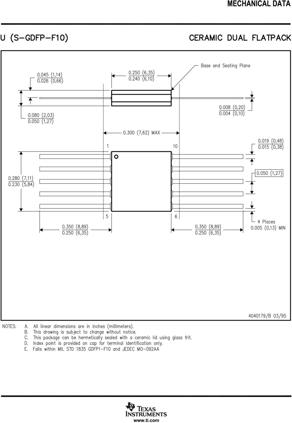
17 MECHANICAL DATA MCER001A JANUARY 1995 REVISED JANUARY 1997 JG (R-GDIP-T8) CERAMIC DUAL-IN-LINE (10,16) (9,00) (7,11) (6,22) (1,65) (1,14) (1,60) (0,38) (0,51) MIN (7,87) (7,37) (5,08) MAX Seating Plane (3,30) MIN (2,54) (0,58) (0,38) (0,36) (0,20) /C 08/96 NOTES: A. All linear dimensions are in inches (millimeters). B. This drawing is subject to change without notice. C. This package can be hermetically sealed with a ceramic lid using glass frit. D. Index point is provided on cap for terminal identification. E. Falls within MIL STD 1835 GDIP1-T8 POST OFFICE BOX DALLAS, TEXAS 75265

18
19

20

21 SCALE PW0008A PACKAGE OUTLINE TSSOP mm max height SMALL OUTLINE PACKAGE 6.6 TYP 6.2 SEATING PLANE C A PIN 1 ID AREA 0.1 C 1 8 6X NOTE 3 2X B NOTE 4 5 8X C A B 1.2 MAX SEE DETAIL A (0.15) TYP 0.25 GAGE PLANE DETAIL A TYPICAL /A 02/2015 NOTES: 1. All linear dimensions are in millimeters. Any dimensions in parenthesis are for reference only. Dimensioning and tolerancing per ASME Y14.5M. 2. This drawing is subject to change without notice. 3. This dimension does not include mold flash, protrusions, or gate burrs. Mold flash, protrusions, or gate burrs shall not exceed 0.15 mm per side. 4. This dimension does not include interlead flash. Interlead flash shall not exceed 0.25 mm per side. 5. Reference JEDEC registration MO-153, variation AA.
22 PW0008A EXAMPLE BOARD LAYOUT TSSOP mm max height SMALL OUTLINE PACKAGE 8X (0.45) 1 8X (1.5) SYMM 8 (R 0.05) TYP SYMM 6X (0.65) 4 5 (5.8) LAND PATTERN EXAMPLE SCALE:10X SOLDER MASK OPENING METAL METAL UNDER SOLDER MASK SOLDER MASK OPENING 0.05 MAX ALL AROUND 0.05 MIN ALL AROUND NON SOLDER MASK DEFINED SOLDER MASK DEFINED SOLDER MASK DETAILS NOT TO SCALE /A 02/2015 NOTES: (continued) 6. Publication IPC-7351 may have alternate designs. 7. Solder mask tolerances between and around signal pads can vary based on board fabrication site.
23 PW0008A EXAMPLE STENCIL DESIGN TSSOP mm max height SMALL OUTLINE PACKAGE 8X (0.45) 1 8X (1.5) SYMM 8 (R 0.05) TYP SYMM 6X (0.65) 4 5 (5.8) SOLDER PASTE EXAMPLE BASED ON mm THICK STENCIL SCALE:10X /A 02/2015 NOTES: (continued) 8. Laser cutting apertures with trapezoidal walls and rounded corners may offer better paste release. IPC-7525 may have alternate design recommendations. 9. Board assembly site may have different recommendations for stencil design.
24
25
26
27
28 IMPORTANT NOTICE Texas Instruments Incorporated and its subsidiaries (TI) reserve the right to make corrections, enhancements, improvements and other changes to its semiconductor products and services per JESD46, latest issue, and to discontinue any product or service per JESD48, latest issue. Buyers should obtain the latest relevant information before placing orders and should verify that such information is current and complete. All semiconductor products (also referred to herein as components ) are sold subject to TI s terms and conditions of sale supplied at the time of order acknowledgment. TI warrants performance of its components to the specifications applicable at the time of sale, in accordance with the warranty in TI s terms and conditions of sale of semiconductor products. Testing and other quality control techniques are used to the extent TI deems necessary to support this warranty. Except where mandated by applicable law, testing of all parameters of each component is not necessarily performed. TI assumes no liability for applications assistance or the design of Buyers products. Buyers are responsible for their products and applications using TI components. To minimize the risks associated with Buyers products and applications, Buyers should provide adequate design and operating safeguards. TI does not warrant or represent that any license, either express or implied, is granted under any patent right, copyright, mask work right, or other intellectual property right relating to any combination, machine, or process in which TI components or services are used. Information published by TI regarding third-party products or services does not constitute a license to use such products or services or a warranty or endorsement thereof. Use of such information may require a license from a third party under the patents or other intellectual property of the third party, or a license from TI under the patents or other intellectual property of TI. Reproduction of significant portions of TI information in TI data books or data sheets is permissible only if reproduction is without alteration and is accompanied by all associated warranties, conditions, limitations, and notices. TI is not responsible or liable for such altered documentation. Information of third parties may be subject to additional restrictions. Resale of TI components or services with statements different from or beyond the parameters stated by TI for that component or service voids all express and any implied warranties for the associated TI component or service and is an unfair and deceptive business practice. TI is not responsible or liable for any such statements. Buyer acknowledges and agrees that it is solely responsible for compliance with all legal, regulatory and safety-related requirements concerning its products, and any use of TI components in its applications, notwithstanding any applications-related information or support that may be provided by TI. Buyer represents and agrees that it has all the necessary expertise to create and implement safeguards which anticipate dangerous consequences of failures, monitor failures and their consequences, lessen the likelihood of failures that might cause harm and take appropriate remedial actions. Buyer will fully indemnify TI and its representatives against any damages arising out of the use of any TI components in safety-critical applications. In some cases, TI components may be promoted specifically to facilitate safety-related applications. With such components, TI s goal is to help enable customers to design and create their own end-product solutions that meet applicable functional safety standards and requirements. Nonetheless, such components are subject to these terms. No TI components are authorized for use in FDA Class III (or similar life-critical medical equipment) unless authorized officers of the parties have executed a special agreement specifically governing such use. Only those TI components which TI has specifically designated as military grade or enhanced plastic are designed and intended for use in military/aerospace applications or environments. Buyer acknowledges and agrees that any military or aerospace use of TI components which have not been so designated is solely at the Buyer's risk, and that Buyer is solely responsible for compliance with all legal and regulatory requirements in connection with such use. TI has specifically designated certain components as meeting ISO/TS16949 requirements, mainly for automotive use. In any case of use of non-designated products, TI will not be responsible for any failure to meet ISO/TS Products Applications Audio Automotive and Transportation Amplifiers amplifier.ti.com Communications and Telecom Data Converters dataconverter.ti.com Computers and Peripherals DLP Products Consumer Electronics DSP dsp.ti.com Energy and Lighting Clocks and Timers Industrial Interface interface.ti.com Medical Logic logic.ti.com Security Power Mgmt power.ti.com Space, Avionics and Defense Microcontrollers microcontroller.ti.com Video and Imaging RFID OMAP Applications Processors TI E2E Community e2e.ti.com Wireless Connectivity Mailing Address: Texas Instruments, Post Office Box , Dallas, Texas Copyright 2016, Texas Instruments Incorporated
Data sheet acquired from Harris Semiconductor SCHS078C -- Revised October 2003
 Data sheet acquired from Harris Semiconductor SCHS078C -- Revised October 2003 The CD4521B types are supplied in 16-lead dual-in-line plastic packages (E suffix), 16-lead small-outline packages (M, M96,
SDLS940A MARCH 1974 REVISED MARCH 1988. Copyright 1988, Texas Instruments Incorporated
 SN5490A, SN5492A, SN5493A, SN54LS90, SN54LS92, SN54LS93 SN7490A, SN7492A, SN7493A, SN74LS90, SN74LS92, SN74LS93 DECADE, DIVIDE-BY-TWELVE AND BINARY COUNTERS SDLS940A MARCH 1974 REVISED MARCH 1988 PRODUCTION
CD4071B Quad 2-Input OR Gate CD4072B Dual 4-Input OR Gate CD4075B Triple 3-Input OR Gate
 Data sheet acquired from Harris Semiconductor SCHS056D Revised August 2003 CD4071B Quad 2-Input OR Gate CD4072B Dual 4-Input OR Gate CD4075B Triple 3-Input OR Gate CD4071B, CD4072B, and CD4075B OR gates
Data sheet acquired from Harris Semiconductor SCHS049C Revised October 2003
 Data sheet acquired from Harris Semiconductor SCHS049C Revised October 2003 CD4060B consists of an oscillator section and 14 ripple-carry binary counter stages. The oscillator configuration allows design
Data sheet acquired from Harris Semiconductor SCHS020C Revised October 2003
 Data sheet acquired from Harris Semiconductor SCHS020C Revised October 2003 The CD4009UB and CD4010B types are supplied in 16-lead hermetic dual-in-line ceramic packages (F3A suffix), 16-lead dual-in-line
Data sheet acquired from Harris Semiconductor SCHS067B Revised July 2003
 Data sheet acquired from Harris Semiconductor SCHS067B Revised July 2003 The CD4502B types are supplied in 16-lead hermetic dual-in-line ceramic packages (F3A suffix), 16-lead dual-in-line plastic packages
with Ultra-Fast Transient Response and High Light-Load Efficiency
 1 Adaptor 6-24V Optional N-FET Driver Ultra-Fast DPM Simplified Application Diagram Iin Ultra-Low Quiescent Current Enhanced Safety Features OCP, OVP, FET Short Support CPU Turbo Mode To System bq24715
 PACKAGE OPTION ADDENDUM www.ti.com 12-Jan-2006 PACKAGING INFORMATION Orderable Device Status (1) Package Type Package Drawing Pins Package Qty Eco Plan (2) Lead/Ball Finish MSL Peak Temp (3) 76005012A
Data sheet acquired from Harris Semiconductor SCHS087D Revised October 2003
 Data sheet acquired from Harris Semiconductor SCHS087D Revised October 2003 The CD4555B and CD4556B types are supplied in 16-lead hermetic dual-in-line ceramic packages (F3A suffix), 16-lead dual-in-line
LM556 LM556 Dual Timer
 LM556 LM556 Dual Timer Literature Number: SNAS549 LM556 Dual Timer General Description The LM556 Dual timing circuit is a highly stable controller capable of producing accurate time delays or oscillation.
TLC556, TLC556Y DUAL LinCMOS TIMERS
 TLC556, TLC556Y DUAL LinCMOS TIMERS ery Low Power Consumption...2 mw Typ at DD = 5 Capable of Operation in Astable Mode CMOS Output Capable of Swinging Rail to Rail High Output-Current Capability Sink
 PACKAGE OPTION ADDENDUM www.ti.com 12-Jan-2006 PACKAGING INFORMATION Orderable Device Status (1) Package Type Package Drawing Pins Package Qty Eco Plan (2) Lead/Ball Finish MSL Peak Temp (3) 5962-9557401QCA
AMC1100: Replacement of Input Main Sensing Transformer in Inverters with Isolated Amplifier
 Application Report SLAA552 August 2012 AMC1100: Replacement of Input Main Sensing Transformer in Inverters with Isolated Amplifier Ambreesh Tripathi and Harmeet Singh Analog/Digital Converters ABSTRACT
PACKAGE OPTION ADDENDUM
 PACKAGE OPTION ADDENDUM www.ti.com 10-Jun-2014 PACKAGING INFORMATION Orderable Device Status (1) Package Type Package Drawing Pins Package Qty Eco Plan (2) Lead/Ball Finish (6) MSL Peak Temp (3) Op Temp
LM5030 LM5030 Application: DC - DC Converter Utilizing the Push-Pull Topology
 LM5030 LM5030 Application: DC - DC Converter Utilizing the Push-Pull Topology Literature Number: SNVA553 LM5030 Application DC DC Converter Utilizing the Push-Pull Topology 1 Push-Pull Topology D1 L +
ORDERING INFORMATION. TOP-SIDE MARKING PDIP N Tube SN74LS07N SN74LS07N PACKAGE. SOIC D Tape and reel SN74LS07DR
 The SN54LS07 and SN74LS17 are obsolete and are no longer supplied. Convert TTL Voltage Levels to MOS Levels High Sink-Current Capability Input Clamping Diodes Simplify System Design Open-Collector Driver
RF37S114 Tag-it HF-I Type 5 NFC, ISO/IEC 15693 Transponder, 4 mm 4 mm
 1 1 Product Folder Sample & Buy Technical Documents Tools & Software Support & Community RF37S114 SCBS907 NOVEMBER 2015 RF37S114 Tag-it HF-I Type 5 NFC, ISO/IEC 15693 Transponder, 4 mm 4 mm 1 Device Overview
1OE 3B NC 3B V GND ORDERING INFORMATION. QFN RGY Tape and reel SN74CBT3125RGYR CU125. SOIC D Tape and reel SN74CBT3125DR
 SN74CBT3125 QUADRUPLE FET BUS SWITCH SCDS021I MAY 1995 REVISED SEPTEMBER 2002 Standard 125-Type Pinout (D, DB, DGV, and PW Packages) 5-Ω Switch Connection Between Two Ports TTL-Compatible Input Levels
SN54LVT574, SN74LVT574 3.3-V ABT OCTAL EDGE-TRIGGERED D-TYPE FLIP-FLOPS WITH 3-STATE OUTPUTS
 SN54LVT574, SN74LVT574 3.3-V ABT OCTAL EDGE-TRIGGERED D-TYPE FLIP-FLOPS WITH 3-STATE OUTPUTS SCBS139D MAY 1992 REVISED JULY 1995 State-of-the-Art Advanced BiCMOS Technology (ABT) Design for 3.3-V Operation
SN55115, SN75115 DUAL DIFFERENTIAL RECEIVERS
 SN55115, SN75115 DUAL DIFFERENTIAL RECEIVERS Choice of Open-Collector or Active Pullup (Totem-Pole) Outputs Single 5-V Supply Differential Line Operation Dual-Channel Operation TTL Compatible ± 15-V Common-Mode
LM709 LM709 Operational Amplifier
 LM709 LM709 Operational Amplifier Literature Number: SNOS659A LM709 Operational Amplifier General Description The LM709 series is a monolithic operational amplifier intended for general-purpose applications
TLC548C, TLC548I, TLC549C, TLC549I 8-BIT ANALOG-TO-DIGITAL CONVERTERS WITH SERIAL CONTROL
 Microprocessor Peripheral or Standalone Operation 8-Bit Resolution A/D Converter Differential Reference Input Voltages Conversion Time...17 µs Max Total Access and Conversion Cycles Per Second TLC548...up
description typical application
 Overvoltage Protection and Lockout for 12 V, 5 V, 3.3 V Undervoltage Protection and Lockout for 5 V and 3.3 V Fault Protection Output With Open-Drain Output Stage Open-Drain Power Good Output Signal for
Application Note AN107
 Murata Balun for CC253x and CC254x LFB182G45BG2D280 By Fredrik Kervel Keywords Balun LFB182G45BG2D280 CC253x CC254x CC257x CC85xx 1 Introduction Murata s LFB182G45BG2D280 integrated balun is specially
description/ordering information
 SLLS047L FEBRUARY 1989 REVISED MARCH 2004 Meets or Exceeds TIA/EIA-232-F and ITU Recommendation V.28 Operates From a Single 5-V Power Supply With 1.0-F Charge-Pump Capacitors Operates Up To 120 kbit/s
54LS174,54LS175,DM54LS174,DM54LS175, DM74LS174,DM74LS175
 54LS174,54LS175,DM54LS174,DM54LS175, DM74LS174,DM74LS175 54LS174 DM54LS174 DM74LS174 54LS175 DM54LS175 DM74LS175 Hex/Quad D Flip-Flops with Clear Literature Number: SNOS290A 54LS174 DM54LS174 DM74LS174
SN54ABT377, SN74ABT377A OCTAL EDGE-TRIGGERED D-TYPE FLIP-FLOPS WITH CLOCK ENABLE
 State-of-the-Art EPIC-ΙΙB BiCMOS Design Significantly Reduces Power Dissipation Latch-Up Performance Exceeds 500 ma Per JEDEC Standard JESD-17 Typical V OLP (Output Ground Bounce) < 1 V at V CC = 5 V,
SN54HC574, SN74HC574 OCTAL EDGE-TRIGGERED D-TYPE FLIP-FLOPS WITH 3-STATE OUTPUTS
 Wide Operating Voltage Range of 2 V to 6 V High-Current 3-State Noninverting Outputs Drive Bus Lines Directly or Up To 15 LSTTL Loads Low Power Consumption, 80-μA Max I CC Typical t pd = 22 ns ±6-mA Output
SN54HC157, SN74HC157 QUADRUPLE 2-LINE TO 1-LINE DATA SELECTORS/MULTIPLEXERS
 SNHC, SNHC QUADRUPLE 2-LINE TO -LINE DATA SELECTORS/MULTIPLEXERS SCLSB DECEMBER 982 REVISED MAY 99 Package Options Include Plastic Small-Outline (D) and Ceramic Flat (W) Packages, Ceramic Chip Carriers
Regulating Pulse Width Modulator
 Regulating Pulse Width Modulator UC1526 FEATURES 8 To 35V Operation 5V Reference Trimmed To ±1% 1Hz To 400kHz Oscillator Range Dual 100mA Source/Sink Outputs Digital Current Limiting Double Pulse Suppression
description/ordering information
 SCES207I APRIL 1999 REVISED SEPTEMBER 2003 Available in the Texas Instruments NanoStar and NanoFree Packages Supports 5-V V CC Operation Inputs Accept Voltages to 5.5 V Max t pd of 6 ns at 3.3 V Low Power
µa7800 SERIES POSITIVE-VOLTAGE REGULATORS
 SLS056J MAY 976 REISED MAY 2003 3-Terminal Regulators Output Current up to.5 A Internal Thermal-Overload Protection High Power-Dissipation Capability Internal Short-Circuit Current Limiting Output Transistor
ESD Protection Exceeds JESD 22 I off. 2000-V Human-Body Model (A114-A) 200-V Machine Model (A115-A)
 200-V Machine Model (A115-A)") www.ti.com FEATURES SN74CBTLV3245A LOW-VOLTAGE OCTAL FET BUS SWITCH SCDS034M JULY 1997 REVISED AUGUST 2005 Standard '245-Type Pinout Latch-Up Performance Exceeds 250 ma Per 5-Ω Switch Connection Between
www.ti.com FEATURES SN74CBTLV3245A LOW-VOLTAGE OCTAL FET BUS SWITCH SCDS034M JULY 1997 REVISED AUGUST 2005 Standard '245-Type Pinout Latch-Up Performance Exceeds 250 ma Per 5-Ω Switch Connection Between
LM388 LM388 1.5W Audio Power Amplifier
 LM388 LM388 1.5W Audio Power Amplifier Literature Number: SNOSBT8A LM388 1 5W Audio Power Amplifier General Description The LM388 is an audio amplifier designed for use in medium power consumer applications
AN-1733 Load Transient Testing Simplified
 Application Report... ABSTRACT The load transient test may be the simplest diagnostic tool available to instantly analyze the loop stability of a system: the visual appearance of the output voltage as
description V CC A CLR BO CO LOAD C D B Q B Q A DOWN UP Q C Q D GND D OR N PACKAGE (TOP VIEW) SDFS031A D3693, JANUARY 1991 REVISED OCTOBER 1993
 SDFS031A D3693, JANUARY 1991 REVISED OCTOBER 1993") High-Speed f max of 100 MHz Typical Parallel Asynchronous Load for Modulo-N Count Lengths Look-Ahead Circuitry Enhances Speed of Cascaded Counters Fully Synchronous in Count Modes Package Optio Include
High-Speed f max of 100 MHz Typical Parallel Asynchronous Load for Modulo-N Count Lengths Look-Ahead Circuitry Enhances Speed of Cascaded Counters Fully Synchronous in Count Modes Package Optio Include
FEATURES DESCRIPTION. www.ti.com SLUS247F APRIL 1997 REVISED NOVEMBER 2007 VDD 8 POWER TO CIRCUITRY. 400 na RES POWER ON RESET 1.
 SLUS247F APRIL 1997 REVISED NOVEMBER 2007 FEATURES Fully Programmable Reset Threshold Fully Programmable Reset Period Fully Programmable Watchdog Period 2% Accurate Reset Threshold Input Voltage Down to
LM138,LM338. LM138/LM338 5-Amp Adjustable Regulators. Literature Number: SNVS771A
 LM138,LM338 LM138/LM338 5-Amp Adjustable Regulators Literature Number: SNVS771A LM138/LM338 5-Amp Adjustable Regulators General Description The LM138 series of adjustable 3-terminal positive voltage regulators
AUDIO DIFFERENTIAL LINE RECEIVER. 0dB (G = 1)
") INA4 INA4 INA4 INA4 INA4 INA4 AUDIO DIFFERENTIAL LINE RECEIVERS db (G = ) FEATURES SINGLE AND DUAL VERSIONS LOW DISTORTION:.% at f = khz HIGH SLEW RATE: 4V/µs FAST SETTLING TIME: µs to.% WIDE SUPPLY RANGE:
INA4 INA4 INA4 INA4 INA4 INA4 AUDIO DIFFERENTIAL LINE RECEIVERS db (G = ) FEATURES SINGLE AND DUAL VERSIONS LOW DISTORTION:.% at f = khz HIGH SLEW RATE: 4V/µs FAST SETTLING TIME: µs to.% WIDE SUPPLY RANGE:
Analysis of Power Supply Topologies for IGBT Gate Drivers in Industrial
 Application Report SLAA672 July 2015 Analysis of Power Supply Topologies for IGBT Gate Drivers in Industrial Sanjay Pithadia, N. Navaneeth Kumar ABSTRACT This application report explains different parameters
SN54HC191, SN74HC191 4-BIT SYNCHRONOUS UP/DOWN BINARY COUNTERS
 Single Down/Up Count-Control Line Look-Ahead Circuitry Enhances Speed of Cascaded Counters Fully Synchronous in Count Modes Asynchronously Presettable With Load Control Package Options Include Plastic
Providing Continuous Gate Drive Using a Charge Pump
 Application Report Philip Meyer and John Tucker... Power Management Products ABSTRACT Certain applications require that output voltage regulation be maintained when the input voltage is only slightly higher
TL081 TL081 Wide Bandwidth JFET Input Operational Amplifier
 TL081 TL081 Wide Bandwidth JFET Input Operational Amplifier Literature Number: SNOSBW6A TL081 Wide Bandwidth JFET Input Operational Amplifier General Description The TL081 is a low cost high speed JFET
CD4051B-Q1, CD4052B-Q1, CD4053B-Q1 CMOS ANALOG MULTIPLEXERS/DEMULTIPLEXERS WITH LOGIC LEVEL CONVERSION
 Features Qualified for Automotive Applications Wide Range of Digital and Analog Signal Levels Digital: V to 0 V Analog: 0 V P-P Low ON Resistance, Ω (Typ) Over V P-P Signal Input Range for = V High OFF
FEATURES APPLICATIONS
 FEATURES DIGITALLY-CONTROLLED ANALOG VOLUME CONTROL: Four Independent Audio Channels Serial Control Interface Zero Crossing Detection Mute Function WIDE GAIN AND ATTENUATION RANGE: +31.5dB to 95.5dB with
AP331A XX G - 7. Lead Free G : Green. Packaging (Note 2)
") Features General Description Wide supply Voltage range: 2.0V to 36V Single or dual supplies: ±1.0V to ±18V Very low supply current drain (0.4mA) independent of supply voltage Low input biasing current:
Features General Description Wide supply Voltage range: 2.0V to 36V Single or dual supplies: ±1.0V to ±18V Very low supply current drain (0.4mA) independent of supply voltage Low input biasing current:
SN28838 PAL-COLOR SUBCARRIER GENERATOR
 Solid-State Reliability Surface-Mount Package NS PACKAE (TOP VIEW) description The SN28838 is a monolithic integrated circuit designed to interface with the SN28837 PALtiming generator in order to generate
LMS8117A LMS8117A 1A Low-Dropout Linear Regulator
 LMS8117A LMS8117A 1A Low-Dropout Linear Regulator Literature Number: SNOS487E LMS8117A 1A Low-Dropout Linear Regulator General Description The LMS8117A is a series of low dropout voltage regulators with
AVAILABLE OPTIONS SMALL OUTLINE (D)
") SLOS65D MARCH 1991 REVISED APRIL 22 2.5-V Virtual Ground for 5-V/GND Analog Systems High Output-Current Capability Sink or Source... 2 ma Typ Micropower Operation... 17 µa Typ Excellent Regulation Characteristics
SLOS65D MARCH 1991 REVISED APRIL 22 2.5-V Virtual Ground for 5-V/GND Analog Systems High Output-Current Capability Sink or Source... 2 ma Typ Micropower Operation... 17 µa Typ Excellent Regulation Characteristics
TS555. Low-power single CMOS timer. Description. Features. The TS555 is a single CMOS timer with very low consumption:
 Low-power single CMOS timer Description Datasheet - production data The TS555 is a single CMOS timer with very low consumption: Features SO8 (plastic micropackage) Pin connections (top view) (I cc(typ)
TSL250, TSL251, TLS252 LIGHT-TO-VOLTAGE OPTICAL SENSORS
 TSL50, TSL5, TLS5 SOES004C AUGUST 99 REVISED NOVEMBER 995 Monolithic Silicon IC Containing Photodiode, Operational Amplifier, and Feedback Components Converts Light Intensity to Output Voltage High Irradiance
AN-225 IC Temperature Sensor Provides Thermocouple Cold-Junction
 Application Report AN-225 IC Temperature Sensor Provides Thermocouple Cold-Junction... ABSTRACT Two circuits using the LM335 for thermocouple cold-junction compensation have been described. With a single
SN74ACT7808 2048 9 STROBED FIRST-IN, FIRST-OUT MEMORY
 Load Clocks and Unload Clocks Can Be Asynchronous or Coincident 2048 Words by 9 Bits Low-Power Advanced CMOS Technology Fast Access Times of 5 ns With a 50-pF Load Programmable Almost-Full/Almost-Empty
SN54LV163A, SN74LV163A 4-BIT SYNCHRONOUS BINARY COUNTERS
 SN54LV163A, SN74LV163A 4-BIT SYNCHRONOUS BINARY COUNTERS 2-V to 5.5-V V CC Operation Max t pd of 9.5 ns at 5 V Typical V OLP (Output Ground Bounce)
Wireless Subwoofer TI Design Tests
 Wireless Subwoofer TI Design Tests This system design was tested for THD+N vs. frequency at 5 watts and 30 watts and THD+N vs. power at 00. Both the direct analog input and the wireless systems were tested.
DS8907 DS8907 AM/FM Digital Phase-Locked Loop Frequency Synthesizer
 DS8907 DS8907 AM/FM Digital Phase-Locked Loop Frequency Synthesizer Literature Number: SNOSBR1A DS8907 AM FM Digital Phase-Locked Loop Frequency Synthesizer General Description The DS8907 is a PLL synthesizer
Multi-Transformer LED TV Power User Guide. Anderson Hsiao
 Multi-Transformer LED TV Power User Guide Anderson Hsiao Operation Range Input Range: 90Vac~264Vac 47Hz~63Hz Dimming Range: Reverse Signal 0V ~ 5V 100Hz ~200Hz 1%~100% Output Range :STBY-5V 20mA~1A 5V
V OUT. I o+ & I o- (typical) 2.3A & 3.3A. Package Type
 2.3A & 3.3A. Package Type") July 25 th, 2012 Automotive Grade AUIRS4427S DUAL LOW SIDE DRIVER Features Gate drive supply range from 6 V to 20 V CMOS Schmitt-triggered inputs 3.3V and 5V logic compatible Two independent gate drivers
July 25 th, 2012 Automotive Grade AUIRS4427S DUAL LOW SIDE DRIVER Features Gate drive supply range from 6 V to 20 V CMOS Schmitt-triggered inputs 3.3V and 5V logic compatible Two independent gate drivers
TSL213 64 1 INTEGRATED OPTO SENSOR
 TSL 64 INTEGRATED OPTO SENSOR SOES009A D4059, NOVEMBER 99 REVISED AUGUST 99 Contains 64-Bit Static Shift Register Contains Analog Buffer With Sample and Hold for Analog Output Over Full Clock Period Single-Supply
LM1851 LM1851 Ground Fault Interrupter
 LM1851 LM1851 Ground Fault Interrupter Literature Number: SNIS158 LM1851 Ground Fault Interrupter General Description The LM1851 is designed to provide ground fault protection for AC power outlets in consumer
CD4049UB, CD4050B. CMOS Hex Buffer/Converters. Applications. [ /Title (CD40 49UB, CD405 0B) /Subject. Ordering Information
 /Subject. Ordering Information") CD4049UB, CD4050B Data sheet acquired from Harris Semiconductor SCHS046I August 1998 - Revised May 2004 [ /Title (CD40 49UB, CD405 0B) /Subject (CMO S Hex Buffer/ Converters) /Autho r () /Keywords (Harris
CD4049UB, CD4050B Data sheet acquired from Harris Semiconductor SCHS046I August 1998 - Revised May 2004 [ /Title (CD40 49UB, CD405 0B) /Subject (CMO S Hex Buffer/ Converters) /Autho r () /Keywords (Harris
AN-311 Theory and Applications of Logarithmic Amplifiers
 Application Report... ABSTRACT A number of instrumentation applications can benefit from the use of logarithmic or exponential signal processing techniques. The design and use of logarithmic/exponential
Application Report. 1 Description of the Problem. Jeff Falin... PMP Portable Power Applications ABSTRACT
 Application Report SLVA255 September 2006 Minimizing Ringing at the Switch Node of a Boost Converter Jeff Falin... PMP Portable Power Applications ABSTRACT This application report explains how to use proper
Design Note DN304. Cebal CCxxxx Development Tools USB Driver Installation Guide By Åsmund B. Bø. Keywords. 1 Introduction
 Cebal CCxxxx Development Tools USB Driver Installation Guide By Åsmund B. Bø Keywords Cebal Driver Windows x86 Windows x64 SmartRF Studio SmartRF Packet Sniffer SmartRF Flash Programmer SmartRF05EB SmartRF04EB
SN55LBC176, SN65LBC176, SN65LBC176Q, SN75LBC176 DIFFERENTIAL BUS TRANSCEIVERS
 Bidirectional Transceiver Meets or Exceeds the Requirements of ANSI Standard TIA/EIA 485 A and ISO 8482:1987(E) High-Speed Low-Power LinBiCMOS Circuitry Designed for High-Speed Operation in Both Serial
LM139/LM239/LM339/LM2901/LM3302 Low Power Low Offset Voltage Quad Comparators
 Low Power Low Offset Voltage Quad Comparators General Description The LM139 series consists of four independent precision voltage comparators with an offset voltage specification as low as 2 mv max for
3V Video Amplifier with 6dB Gain and Filter in SC70
 OPA360 SB0S294E DECEMBER 2003 REVISED SEPTEMBER 2006 3V Video Amplifier with 6dB Gain and Filter in SC70 FEATURES EXCELLENT VIDEO PERFORMANCE INTERNAL GAIN: 6dB 2-POLE RECONSTRUCTION FILTER SAG CORRECTION
SN74ACT7807 2048 9 CLOCKED FIRST-IN, FIRST-OUT MEMORY
 Free-Running Read and Write Clocks Can Be Asynchronous or Coincident Read and Write Operations Synchronized to Independent System Clocks Input-Ready Flag Synchronized to Write Clock Output-Ready Flag Synchronized
TMP100 EP DIGITAL TEMPERATURE SENSOR WITH I 2 C INTERFACE
 Controlled Baseline One Assembly/Test Site, One Fabrication Site Enhanced Diminishing Manufacturing Sources (DMS) Support Enhanced Product-Change Notification Qualification Pedigree Digital Output: I 2
AP1509. 150KHz, 2A PWM BUCK DC/DC CONVERTER. Description. Pin Assignments V IN. Applications. Features. (Top View) GND GND. Output AP1509 GND GND
 GND GND. Output AP1509 GND GND") Description Pin Assignments The series are monolithic IC designed for a stepdown DC/DC converter, and own the ability of driving a 2A load without additional transistor. It saves board space. The external
Description Pin Assignments The series are monolithic IC designed for a stepdown DC/DC converter, and own the ability of driving a 2A load without additional transistor. It saves board space. The external
TPS76901, TPS76912, TPS76915, TPS76918, TPS76925 TPS76927, TPS76928, TPS76930, TPS76933, TPS76950 ULTRALOW-POWER 100-mA LOW-DROPOUT LINEAR REGULATORS
 -ma Low-Dropout Regulator TPS76901, TPS76912, TPS76915, TPS76918, TPS76925 TPS76927, TPS76928, TPS76930,, TPS76950 ULTRALOW-POWER -ma LOW-DROPOUT LINEAR REGULATORS Available in 1.2-V, 1.5-V, 1.8-V, 2.5-V,
Importing a SPICE NetList Into TINA9-TI
 Application Report Importing a SPICE NetList into TINA9-TI John Miller... Analog elab ABSTRACT This application note describes the procedure for importing an unencrypted SPICE netlist into TINA9-TI (available
Design Note DN041. Using CC253X or CC254X with Dipole PCB Antennas. Keywords. 1 Introduction. By Espen Wium CC2530 CC2531 CC2533 CC2540 CC2541
 Using CC253X or CC254X with Dipole PCB Antennas By Espen Wium Keywords Half wave dipole RF Antenna Efficiency Gain TRP (Total Radiated Power) CC2530 CC2531 CC2533 CC2540 CC2541 1 Introduction Many RFICs
Stereo Audio Volume Control
 PGA2320 Stereo Audio Volume Control FEATURES DIGITALLY-CONTROLLED ANALOG VOLUME CONTROL: Two Independent Audio Channels Serial Control Interface Zero Crossing Detection Mute Function WIDE GAIN AND ATTENUATION
Precision, Unity-Gain Differential Amplifier AMP03
 a FEATURES High CMRR: db Typ Low Nonlinearity:.% Max Low Distortion:.% Typ Wide Bandwidth: MHz Typ Fast Slew Rate: 9.5 V/ s Typ Fast Settling (.%): s Typ Low Cost APPLICATIONS Summing Amplifiers Instrumentation
OLF500: High CMR, High-Speed Logic Gate Hermetic Surface Mount Optocoupler
 TM DATA SHEET OLF500: High CMR, High-Speed Logic Gate Hermetic Surface Mount Optocoupler Features Hermetic SMT flat-pack package Electrical parameters guaranteed over 55 C to +125 C ambient temperature
Texas Instruments. FB PS LLC Test Report HVPS SYSTEM AND APPLICATION TEAM REVA
 Texas Instruments FB PS LLC Test Report HVPS SYSTEM AND APPLICATION TEAM REVA 12/05/2014 1 General 1.1 PURPOSE Provide the detailed data for evaluating and verifying the FB-PS-LLC. The FB-PS-LLC is a Full
Hex buffer with open-drain outputs
 Rev. 5 27 October 20 Product data sheet. General description The provides six non-inverting buffers. The outputs are open-drain and can be connected to other open-drain outputs to implement active-low
Ultrasonic Sensing Basics for Liquid Level Sensing, Flow Sensing, and Fluid
 Application Report SNAA0A March 015 Revised June 015 Ultrasonic Sensing Basics for Liquid Level Sensing, Flow Sensing, and Fluid AmyLe ABSTRACT The need for accurate and reliable sensors is growing in
Quad 2-input NAND Schmitt trigger
 Rev. 9 15 December 2015 Product data sheet 1. General description 2. Features and benefits 3. Applications The is a quad two-input NAND gate. Each input has a Schmitt trigger circuit. The gate switches
TS321 Low Power Single Operational Amplifier
 SOT-25 Pin Definition: 1. Input + 2. Ground 3. Input - 4. Output 5. Vcc General Description The TS321 brings performance and economy to low power systems. With high unity gain frequency and a guaranteed
ICS650-44 SPREAD SPECTRUM CLOCK SYNTHESIZER. Description. Features. Block Diagram DATASHEET
 DATASHEET ICS650-44 Description The ICS650-44 is a spread spectrum clock synthesizer intended for video projector and digital TV applications. It generates three copies of an EMI optimized 50 MHz clock
AN-1900 LM3150 Evaluation Boards
 User's Guide 1 Introduction The LM3150 evaluation boards are designed to provide the design engineer with a fully functional power converter based on Constant On-Time with Emulated Ripple mode control
LM2900,LM3301,LM3900. LM2900/LM3900/LM3301 Quad Amplifiers. Literature Number: SNOSBV6
 LM2900,LM3301,LM3900 LM2900/LM3900/LM3301 Quad Amplifiers Literature Number: SNOSBV6 LM2900/LM3900/LM3301 Quad Amplifiers General Description The LM2900 series consists of four independent, dual input,
MC33064DM 5 UNDERVOLTAGE SENSING CIRCUIT
 Order this document by MC3464/D The MC3464 is an undervoltage sensing circuit specifically designed for use as a reset controller in microprocessor-based systems. It offers the designer an economical solution
Wide Bandwidth, Fast Settling Difet OPERATIONAL AMPLIFIER
 Wide Bandwidth, Fast Settling Difet OPERATIONAL AMPLIFIER FEATURES HIGH GAIN-BANDWIDTH: 35MHz LOW INPUT NOISE: 1nV/ Hz HIGH SLEW RATE: V/µs FAST SETTLING: 24ns to.1% FET INPUT: I B = 5pA max HIGH OUTPUT
16-Bit DIGITAL-TO-ANALOG CONVERTER With Serial Data Interface
 SBAS0A JULY 997 REVISED NOVEMBER 00 -Bit DIGITAL-TO-ANALOG CONVERTER With Serial Data Interface FEATURES: SERIAL DIGITAL INTERFACE VOLTAGE OUTPUT: ±0V, ±V, 0 to +0V ± LSB INTEGRAL LINEARITY -BIT MONOTONIC
PDS5100H. Product Summary. Features and Benefits. Mechanical Data. Description and Applications. Ordering Information (Note 5) Marking Information
 Marking Information") Green 5A HIGH VOLTAGE SCHOTTKY BARRIER RECTIFIER POWERDI 5 Product Summary I F V R V F MAX (V) I R MAX (ma) (V) (A) @ +25 C @ +25 C 1 5..71.35 Description and Applications This Schottky Barrier Rectifier
Green 5A HIGH VOLTAGE SCHOTTKY BARRIER RECTIFIER POWERDI 5 Product Summary I F V R V F MAX (V) I R MAX (ma) (V) (A) @ +25 C @ +25 C 1 5..71.35 Description and Applications This Schottky Barrier Rectifier
74HCU04. 1. General description. 2. Features and benefits. 3. Ordering information. Hex unbuffered inverter
 Rev. 7 8 December 2015 Product data sheet 1. General description The is a hex unbuffered inverter. Inputs include clamp diodes. This enables the use of current limiting resistors to interface inputs to
4-bit binary full adder with fast carry CIN + (A1 + B1) + 2(A2 + B2) + 4(A3 + B3) + 8(A4 + B4) = = S1 + 2S2 + 4S3 + 8S4 + 16COUT
 + 2(A2 + B2) + 4(A3 + B3) + 8(A4 + B4) = = S1 + 2S2 + 4S3 + 8S4 + 16COUT") Rev. 03 11 November 2004 Product data sheet 1. General description 2. Features The is a high-speed Si-gate CMOS device and is pin compatible with low power Schottky TTL (LSTTL). The is specified in compliance
Rev. 03 11 November 2004 Product data sheet 1. General description 2. Features The is a high-speed Si-gate CMOS device and is pin compatible with low power Schottky TTL (LSTTL). The is specified in compliance
TI Designs Precision: Verified Design Comparator with Hysteresis Reference Design
 TI Designs Precision: Verified Design Comparator with Hysteresis Reference Design Art Kay, Timothy Claycomb TI Designs Precision TI Designs Precision are analog solutions created by TI s analog experts.
AN-1963 IEEE 1588 Synchronization Over Standard Networks Using the
 Application Report AN-963 IEEE 588 Synchronization Over Standard Networks Using the... ABSTRACT This application report describes a method of synchronization that provides much more accurate synchronization
AP1506. 150KHz, 3A PWM BUCK DC/DC CONVERTER. Pin Assignments. Description. Features. Applications. ( Top View ) 5 SD 4 FB 3 Gnd 2 Output 1 V IN
 5 SD 4 FB 3 Gnd 2 Output 1 V IN") Description Pin Assignments The series are monolithic IC designed for a stepdown DC/DC converter, and own the ability of driving a 3A load without external transistor. Due to reducing the number of external
Description Pin Assignments The series are monolithic IC designed for a stepdown DC/DC converter, and own the ability of driving a 3A load without external transistor. Due to reducing the number of external
www.jameco.com 1-800-831-4242
 Distributed by: www.jameco.com 1-800-831-4242 The content and copyrights of the attached material are the property of its owner. LF411 Low Offset, Low Drift JFET Input Operational Amplifier General Description
APPLICATION NOTE BUILDING A QAM MODULATOR USING A GC2011 DIGITAL FILTER CHIP
 SLWA022 APPLICATION NOTE BUILDING A QAM MODULATOR USING A GC2011 DIGITAL CHIP October 6, 1994 1.0 INTRODUCTION This report describes how one can use the GC2011 Digital Filter chip to build digital modulators
August 2001 PMP Low Power SLVU051
 User s Guide August 2001 PMP Low Power SLVU051 IMPORTANT NOTICE Texas Instruments and its subsidiaries (TI) reserve the right to make changes to their products or to discontinue any product or service
High-Voltage, Internally Powered ISOLATION AMPLIFIER
 ISO17 High-Voltage, Internally Powered ISOLATION AMPLIFIER FEATURES SIGNAL AND POWER IN ONE TRIPLE-WIDE PACKAGE 8Vpk TEST VOLTAGE 5Vrms CONTINUOUS AC BARRIER RATING WIDE INPUT SIGNAL RANGE: 1V to 1V WIDE
HEF4011B. 1. General description. 2. Features and benefits. 3. Ordering information. 4. Functional diagram. Quad 2-input NAND gate
 Rev. 6 10 December 2015 Product data sheet 1. General description 2. Features and benefits 3. Ordering information The is a quad 2-input NAND gate. The outputs are fully buffered for the highest noise
INSTRUMENTATION AMPLIFIER With Precision Voltage Reference
 INSTRUMENTATION AMPLIFIER With Precision Voltage Reference FEATURES LOW QUIESCENT CURRENT: 46µA PRECISION VOLTAGE REFERENCE: 1.24V, 2.V, V or 1V SLEEP MODE LOW OFFSET VOLTAGE: 2µV max LOW OFFSET DRIFT:
NTMS4920NR2G. Power MOSFET 30 V, 17 A, N Channel, SO 8 Features
 NTMS9N Power MOSFET 3 V, 7 A, N Channel, SO Features Low R DS(on) to Minimize Conduction Losses Low Capacitance to Minimize Driver Losses Optimized Gate Charge to Minimize Switching Losses These Devices