ADS1251EVM FEATURES DESCRIPTION
|
|
|
- Horace Thomas
- 9 years ago
- Views:
Transcription
1 SBAU041 MARCH 2001 FEATURES PROVIDES FAST AND EASY PERFORMANCE TESTING FOR ADS1251 PC SERIAL PORT CONTROL WINDOWS 95/98 SOFTWARE Windows is a registered trademark of Microsoft Corp. DESCRIPTION The demo board is designed for ease of use when evaluating the high-resolution analog-to-digital converter ADS1251. The ADS1251 offers 24-bits No Missing Codes performance. It has one differential input channel. The ADS1251 features a synchronous serial interface. It has been designed for closed-loop control applications in the industrial process market and high-resolution applications in the test and measurement market. It is also ideal for remote applications, battery-powered instruments, and isolated systems. Note: The ADS1251 and ADS1252 will both work in the ADS1252EVM. The uses the same board as the ADS1252EVM. Please be aware that an important notice concerning availability, standard warranty, and use in critical applications of Texas Instruments semiconductor products and disclaimers thereto appears at the end of this data sheet. PRODUCTION DATA information is current as of publication date. Products conform to specifications per the terms of Texas Instruments standard warranty. Production processing does not necessarily include testing of all parameters. Copyright 2001, Texas Instruments Incorporated

2 INITIAL CONFIGURATION The is designed to be operational without any user configuration except for connecting power supplies and the communications cable to the PC serial port. Jumpers JMP1 (Clock Oscillator), JMP3 (DUT clock), JMP8 (ADS1251 power), and JMP10 (reference select) have already been installed. POWER SUPPLY The demo board is powered from an 8V to 12V power source. That voltage is regulated to 5V for use of the ADS1251 and the microprocessor. VOLTAGE REFERENCE Jumper JMP10 is used to select the source for the reference voltage. If the jumper is placed on the two pins closest to the BNC connector, the BNC connector will be selected as the source of the reference voltage. If the jumper is placed on the two pins away from the connector, then the on-board 4.096V reference is chosen. The selected voltage is buffered with an OPA350 op amp for the use of the ADS1251. CLOCK The 50MHz crystal oscillator provides the operating frequency for the microprocessor. The processor in combination with a PLL provides a clock for the ADS1251. PC BOARD LAYOUT The demo board consists of a four-layer PC board. To achieve the highest level of performance, surfacemount components are used wherever possible. This reduces the trace length and minimizes the effects of parasitic capacitance and inductance. The demo board has a split ground plane with all the analog signals over one portion and the digital signals in the other. Keep in mind that this approach may not necessarily yield optimum performance results when designing the ADS1251 into different individual applications. In any case, thoroughly bypassing the power supply and reference pins of the converter is strongly recommended. WINDOWS SOFTWARE The serial port used for communications can be specified on the command line. Just add port1, port2, etc. after the command in the Target field, as shown in Figure 1. It can also be specified in the program. The ADS1251 is very easy to use. Basically, supply a clock and read the output data. The Evaluation software provides a convienent method to vary the operation and observe the results. It also can display the results of acquired data and perform a frequency analysis. FIGURE 1. Demo Properties. The program has two windows: 1) The Control Window and 2) The Data Display Window. The Control Window can Acquire data, set the frequency for data acquisition and select the PC communications port. In the Get Data screen, shown in Figure 2, the number of samples can be set from 32 to points. Each data point can be raw data from the ADS1251 or the points can be the result of averages of the Analog-to-Digital (A/D) converter data. Up to 32,768 averages can be performed for each output data point. FIGURE 2. Initial Control Window. The Power Down button will put the part into a low-power state. Collect Data will return the part to the full-power state. The power-down state will only reduce the demo board current by about 1mA. For detailed power analysis, use JMP8 to power the part from an external source. 2 SBAU041

3 The Frequency screen, shown in Figure 3, lets you choose the operating frequency of the device. The frequencies of 2kHz and 10kHz give good noise performance. Although, by selecting Variable Sample Rate, other sample rates can be selected by choosing the output sample rate or the clock frequency (Sample Rate 384). The maximum recommended frequency for the ADS1251 is 8MHz or a sample rate of 20.8kHz. The noise is not as good when using the Variable Sample Rate because of the PLL used to generate the clocks. Along the top of the Time Domain Display, shown in Figure 5, are icons that can be used to select the various display modes. The four displays are 1) Time Domain, 2) FFT, 3) Histogram and 4) Data List. Statistics for the data are also displayed on the top of the Time Domain Display. It shows the Standard Deviation, Mean, Maximum, and Minimum. FIGURE 5. Time Domain Display. FIGURE 3. Frequency Screen. The Options screen, shown in Figure 4, gives you control of which serial port the program will use when it communicates with the evaluation module. This is also where you specify the reference voltage used to normalize the data for a scaled by LSB voltage display. Several figures of merit are computed from the FFT information shown in Figure 6. These include the Signal to Noise Ratio (SNR), Signal to Noise plus Distortion (SINAD), Total Harmonic Distortion (THD) and Spurious Free Dynamic Range (SFDR). FIGURE 4. Configuration Window. FIGURE 6. FFT Display. SBAU041 3

4 There are many options for the FFT display. The options menu selection opens the screen shown in Figure 7. Several windows are provided to modify the data before the FFT computation. Additionally, the FFT display can mark some features such as the main frequency and the harmonics. Finally, the data can be analyzed in detail with the Data List display shown in Figure 8. The Data Formats can be selected. This selection will also be used for the display of the date in the Time Domain display. The Scaled by LSB converts the data to a voltage with the assumption that the voltage reference is as defined in Figure 4. FIGURE 7. FFT Options. FIGURE 8. Data List Display. 4 SBAU041

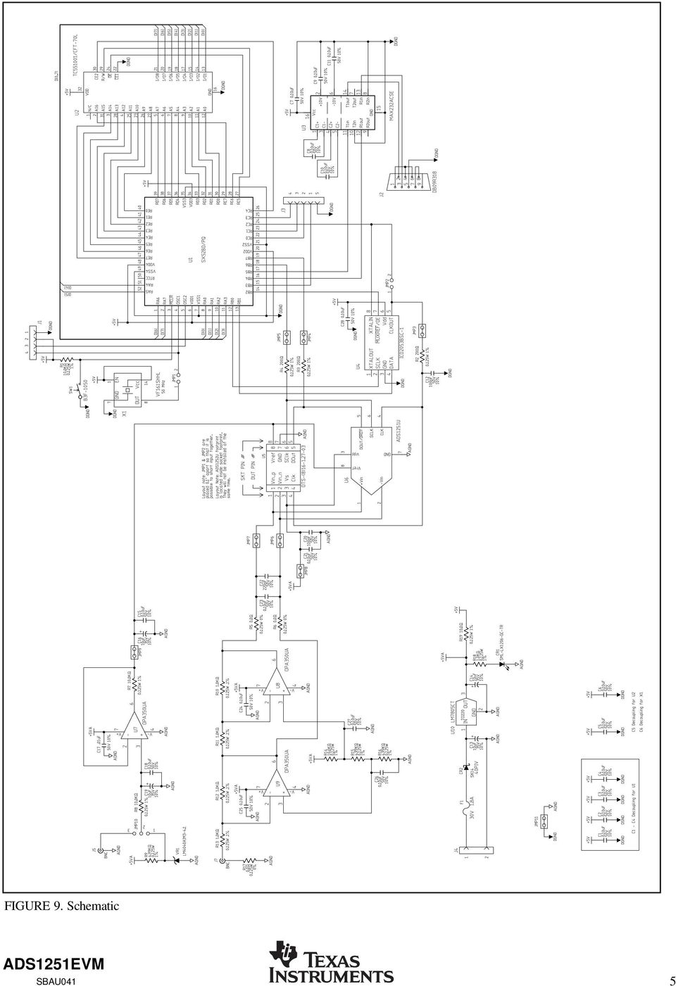
5 FIGURE 9. Schematic SBAU041 5
6 COMPONENT LIST PART NUMBER DESCRIPTION REF. DES. QTY VENDOR PART NUMBER MANUFACTURER ADS1251U IC, A/D CONV, 24-BIT,20kHz U6 1 ADS1251U B3F-1050 SWITCH, SPST, PB-MOM SW1 1 B3F-1050 CRCW120610R0F RES, 10.0Ω, 0.125W, 1%, CHIP-THICK-FILM R 19 1 CRCW120610R0F DALE CRCW RES, 0.0Ω, 0.125W, 0%, CHIP-JUMPER R 5,R 6,R 17 3 CRCW DALE CRCW F RES, 1.0kΩ, 0.125W,.1%, CHIP-THICK-FILM R 18 1 CRCW F DALE CRCW F RES, 10.0kΩ, 0.125W, 1%, CHIP-THICK-FILM R 1,R 7,R 8,R 14 4 CRCW F DALE CRCW RES, 200Ω, 0.125W, 1%, CHIP-THICK-FILM R 2,R 3,R 4 3 CRCW F DALE CRCW F RES, 4.99kΩ, 0.125W, 1%, CHIP-THICK-FILM R 9,R 15,R 16 3 CRCW F DALE C1206C101K5GAC CAP, 100pF, 50V, 10%, CHIP-CERAMIC COG C 12,C 20 2 C1206C101K5GAC KEMET C1206C103K5RAC CAP,.01uF, 50V, 10%, CHIP-CERAMIC X7R C 17 1 C1206C103K5RAC KEMET C1206C104K5RAC CAP, 0.10uF, 50V, 10%, CHIP-CERAMIC X7R C 1,C 2,C 3,C 4,C 5,C 6 20 C1206C104K5RAC KEMET * C 7,C 8,C 9,C 10,C 11 * C 15,C 18,C 21,C 23,C 24 * C 25,C 26,C 27,C 28 C1206C221K5GAC CAP, 220pF, 50V, 10%, CHIP-CERAMIC COG C 22 1 C1206C221K5GAC KEMET ICD2053BSC-1 IC, PROGRAMMABLE CLOCK GENERATOR U4 1 ICD2053BSC-1 LM4040AIM3-4.1 IC, PREC. V REF 4.1V, 0.1% SOT-23 VR1 1 LM4040AIM3-4.1 LM7805CT 3-TERM. 5V/1A POS. FIXED REGULATOR, T U10 1 LM7805CT National Semi MAX232ACSE IC, DRVR/RCVR, RS V U3 1 MAX232ACSE OPA350UA OPAMP, CMOS, SINGLE-SUPPLY U7,U8,U9 1 OTS-(8) RUE090 FUSE, 30V, RESETTABLE POLYSWITCH F1 1 RUE090 SK14 DIODE, SCHOTTKEY, 40PIV,1.0A CR2 1 SK14 SML-LX1206-GC-TR LED, SMT 1206, GREEN CR1 1 SML-LX1206-GC-TR SX52BD/PQ IC, uproc, 4k WORD 50MHz. U1 1 SX52BD/PQ TC551001/CFT-70L IC, MEMORY 1Mb X 8-BIT SRAM U2 1 TC551001/CFT-70L TNPW B RES 1k 1/8W.1% R 10,R 11,R 12,R 4 TNPW B TSW L-S CONN, 2 POS.1 CTR.025 SQ. POST JMP1,JMP2,JMP3,JMP4 10 TSW L-S * JMP5,JMP6,JMP7,JMP8 * JMP9,JMP11 TSW L-S CONN, 3 POS.1 CTR.025 SQ. POST JMP10 1 TSW L-S TSW L-S CONN, 4 POS.1 CTR.025 SQ. POST J1 1 TSW L-S TSW L-S CONN, 5 POS.1 CTR.025 SQ. POST J3 1 TSW L-S T491D106K035AS CAP, 10uF, 35V, 10%, TANTALUM CHIP-MOLDED C 13,C 14,C 16,C 19p 4 T491D106K035AS KEMET VF161SHHL IC, HYBRID XTAL OSC,VERY HI SPEED X1 1 VF161SHHL 2SV-02 TERM. BLK, 2 POS LEVER POWER CONNECTOR J4 1 2SV CONN, JACK, BNC, PCB MNT, VERTICAL, 50Ω J5,J CONN, DB9, RECPT.318 STYLE WITH STD HDWR J Total Parts Used: 80 6 SBAU041

7 IMPORTANT NOTICE Texas Instruments and its subsidiaries (TI) reserve the right to make changes to their products or to discontinue any product or service without notice, and advise customers to obtain the latest version of relevant information to verify, before placing orders, that information being relied on is current and complete. All products are sold subject to the terms and conditions of sale supplied at the time of order acknowledgment, including those pertaining to warranty, patent infringement, and limitation of liability. TI warrants performance of its products to the specifications applicable at the time of sale in accordance with TI s standard warranty. Testing and other quality control techniques are utilized to the extent TI deems necessary to support this warranty. Specific testing of all parameters of each device is not necessarily performed, except those mandated by government requirements. Customers are responsible for their applications using TI components. In order to minimize risks associated with the customer s applications, adequate design and operating safeguards must be provided by the customer to minimize inherent or procedural hazards. TI assumes no liability for applications assistance or customer product design. TI does not warrant or represent that any license, either express or implied, is granted under any patent right, copyright, mask work right, or other intellectual property right of TI covering or relating to any combination, machine, or process in which such products or services might be or are used. TI s publication of information regarding any third party s products or services does not constitute TI s approval, license, warranty or endorsement thereof. Reproduction of information in TI data books or data sheets is permissible only if reproduction is without alteration and is accompanied by all associated warranties, conditions, limitations and notices. Representation or reproduction of this information with alteration voids all warranties provided for an associated TI product or service, is an unfair and deceptive business practice, and TI is not responsible nor liable for any such use. Resale of TI s products or services with statements different from or beyond the parameters stated by TI for that product or service voids all express and any implied warranties for the associated TI product or service, is an unfair and deceptive business practice, and TI is not responsible nor liable for any such use. Also see: Standard Terms and Conditions of Sale for Semiconductor Products. Mailing Address: Texas Instruments Post Office Box Dallas, Texas Copyright 2001, Texas Instruments Incorporated

SDLS068A DECEMBER 1972 REVISED OCTOBER 2001. Copyright 2001, Texas Instruments Incorporated
 SN54174, SN54175, SN54LS174, SN54LS175, SN54S174, SN54S175, SN74174, SN74175, SN74LS174, SN74LS175, SN74S174, SN74S175 PRODUCTION DATA information is current as of publication date. Products conform to
August 2001 PMP Low Power SLVU051
 User s Guide August 2001 PMP Low Power SLVU051 IMPORTANT NOTICE Texas Instruments and its subsidiaries (TI) reserve the right to make changes to their products or to discontinue any product or service
SN54165, SN54LS165A, SN74165, SN74LS165A PARALLEL-LOAD 8-BIT SHIFT REGISTERS
 The SN54165 and SN74165 devices SN54165, SN54LS165A, SN74165, SN74LS165A PRODUCTION DATA information is current as of publication date. Products conform to specifications per the terms of Texas Instruments
Designing Gain and Offset in Thirty Seconds
 Application Report SLOA097 February 2002 Designing Gain and Offset in Thirty Seconds Bruce Carter High Performance Linear ABSTRACT This document discusses how to design an operational amplifier (op amp)
Controlling TAS5026 Volume After Error Recovery
 Application Report SLEA009 March 2003 Controlling TAS5026 Volume After Error Recovery Jorge S. Melson Hwang Soo, Son HPA Digital Audio Applications ABSTRACT The TAS5026 monitors the relationship between
Current-Transformer Phase-Shift Compensation and Calibration
 Application Report SLAA122 February 2001 Current-Transformer Phase-Shift Compensation and Calibration Kes Tam Mixed Signal Products ABSTRACT This application report demonstrates a digital technique to
How To Close The Loop On A Fully Differential Op Amp
 Application Report SLOA099 - May 2002 Fully Differential Op Amps Made Easy Bruce Carter High Performance Linear ABSTRACT Fully differential op amps may be unfamiliar to some designers. This application
Pressure Transducer to ADC Application
 Application Report SLOA05 October 2000 Pressure Transducer to ADC Application John Bishop ABSTRACT Advanced Analog Products/OpAmp Applications A range of bridgetype transducers can measure numerous process
Application Report. 1 Description of the Problem. Jeff Falin... PMP Portable Power Applications ABSTRACT
 Application Report SLVA255 September 2006 Minimizing Ringing at the Switch Node of a Boost Converter Jeff Falin... PMP Portable Power Applications ABSTRACT This application report explains how to use proper
Filter Design in Thirty Seconds
 Application Report SLOA093 December 2001 Filter Design in Thirty Seconds Bruce Carter High Performance Analog ABSTRACT Need a filter fast? No theory, very little math just working filter designs, and in
Application Report. 1 Introduction. 2 Resolution of an A-D Converter. 2.1 Signal-to-Noise Ratio (SNR) Harman Grewal... ABSTRACT
 Harman Grewal... ABSTRACT") Application Report SLAA323 JULY 2006 Oversampling the ADC12 for Higher Resolution Harman Grewal... ABSTRACT This application report describes the theory of oversampling to achieve resolutions greater than
Application Report SLAA323 JULY 2006 Oversampling the ADC12 for Higher Resolution Harman Grewal... ABSTRACT This application report describes the theory of oversampling to achieve resolutions greater than
SINGLE-SUPPLY OPERATION OF OPERATIONAL AMPLIFIERS
 SINGLE-SUPPLY OPERATION OF OPERATIONAL AMPLIFIERS One of the most common applications questions on operational amplifiers concerns operation from a single supply voltage. Can the model OPAxyz be operated
Wide Bandwidth, Fast Settling Difet OPERATIONAL AMPLIFIER
 Wide Bandwidth, Fast Settling Difet OPERATIONAL AMPLIFIER FEATURES HIGH GAIN-BANDWIDTH: 35MHz LOW INPUT NOISE: 1nV/ Hz HIGH SLEW RATE: V/µs FAST SETTLING: 24ns to.1% FET INPUT: I B = 5pA max HIGH OUTPUT
Using the Texas Instruments Filter Design Database
 Application Report SLOA062 July, 2001 Bruce Carter Using the Texas Instruments Filter Design Database High Performance Linear Products ABSTRACT Texas Instruments applications personnel have decades of
Motor Speed Measurement Considerations When Using TMS320C24x DSPs
 Application Report SPRA771 - August 2001 Motor Speed Measurement Considerations When Using TMS320C24x DSPs Shamim Choudhury DCS Applications ABSTRACT The TMS320C24x generation of DSPs provide appropriate
RETRIEVING DATA FROM THE DDC112
 RETRIEVING DATA FROM THE by Jim Todsen This application bulletin explains how to retrieve data from the. It elaborates on the discussion given in the data sheet and provides additional information to allow
APPLICATION BULLETIN
 APPLICATION BULLETIN Mailing Address: PO Box 11400 Tucson, AZ 85734 Street Address: 6730 S. Tucson Blvd. Tucson, AZ 85706 Tel: (602 746-1111 Twx: 910-952-111 Telex: 066-6491 FAX (602 889-1510 Immediate
WHAT DESIGNERS SHOULD KNOW ABOUT DATA CONVERTER DRIFT
 WHAT DESIGNERS SHOULD KNOW ABOUT DATA CONVERTER DRIFT Understanding the Components of Worst-Case Degradation Can Help in Avoiding Overspecification Exactly how inaccurate will a change in temperature make
Audio Tone Control Using The TLC074 Operational Amplifier
 Application Report SLOA42 - JANUARY Audio Tone Control Using The TLC74 Operational Amplifier Dee Harris Mixed-Signal Products ABSTRACT This application report describes the design and function of a stereo
SN28838 PAL-COLOR SUBCARRIER GENERATOR
 Solid-State Reliability Surface-Mount Package NS PACKAE (TOP VIEW) description The SN28838 is a monolithic integrated circuit designed to interface with the SN28837 PALtiming generator in order to generate
APPLICATION BULLETIN
 APPLICATION BULLETIN Mailing Address: PO Box 11400, Tucson, AZ 85734 Street Address: 6730 S. Tucson Blvd., Tucson, AZ 85706 Tel: (520) 746-1111 Telex: 066-6491 FAX (520) 889-1510 Product Info: (800) 548-6132
High-Speed Gigabit Data Transmission Across Various Cable Media at Various Lengths and Data Rate
 Application Report SLLA091 - November 2000 High-Speed Gigabit Data Transmission Across Various Cable Media at Various Lengths and Data Rate Boyd Barrie, Huimin Xia ABSTRACT Wizard Branch, Bus Solution
Design Note DN004. Folded Dipole Antenna for CC25xx By Audun Andersen. Keywords. 1 Introduction CC2500 CC2550 CC2510 CC2511
 Folded Dipole Antenna for CC25xx By Audun Andersen Keywords CC2500 CC2550 CC2510 CC2511 Folded Dipole PCB Antenna 2.4 GHz 1 Introduction This document describes a folded dipole PCB antenna design that
THE RIGHT-HALF-PLANE ZERO --A SIMPLIFIED EXPLANATION
 THE RGHT-HALF-PLANE ZERO --A SMPLFED EXPLANATON n small signal loop analysis, poles and zeros are normally located in the left half of the complex s-plane. The Bode plot of a conventional or lefthalf-plane
CUSTOM GOOGLE SEARCH PRO. User Guide. User Guide Page 1
 CUSTOM GOOGLE SEARCH PRO User Guide User Guide Page 1 Important Notice reserves the right to make corrections, modifications, enhancements, improvements, and other changes to its products and services
Application Report SLVA051
 Application Report November 998 Mixed-Signal Products SLVA05 ltage Feedback Vs Current Feedback Op Amps Application Report James Karki Literature Number: SLVA05 November 998 Printed on Recycled Paper IMPORTANT
Simplifying System Design Using the CS4350 PLL DAC
 Simplifying System Design Using the CS4350 PLL 1. INTRODUCTION Typical Digital to Analog Converters (s) require a high-speed Master Clock to clock their digital filters and modulators, as well as some
TI and ibiquity Introduce Industry s Lowest Cost Single-Chip AM/FM and HD Radio Baseband John Gardner Digital Radio Marketing Manager
 TI and ibiquity Introduce Industry s Lowest Cost Single-Chip AM/FM and HD Radio Baseband John Gardner Digital Radio Marketing Manager SPRT328 HD Radio Products Planned Trunk mounted HD Radio receiver at
PCIe XMC x8 Lane Adapter
 Adapts PCI Express XMC to Desktop with P16 High Speed Communications Ports and JN4 Digital IO FEATURES Adapt one XMC PCI Express VITA 42.3 module to a desktop PCI Express slot Supports up to 8 lanes Transparent
Wireless Subwoofer TI Design Tests
 Wireless Subwoofer TI Design Tests This system design was tested for THD+N vs. frequency at 5 watts and 30 watts and THD+N vs. power at 00. Both the direct analog input and the wireless systems were tested.
Signal Conditioning Wheatstone Resistive Bridge Sensors
 Application Report SLOA034 - September 1999 Signal Conditioning Wheatstone Resistive Bridge Sensors James Karki Mixed Signal Products ABSTRACT Resistive elements configured as Wheatstone bridge circuits
Application Note AN107
 Murata Balun for CC253x and CC254x LFB182G45BG2D280 By Fredrik Kervel Keywords Balun LFB182G45BG2D280 CC253x CC254x CC257x CC85xx 1 Introduction Murata s LFB182G45BG2D280 integrated balun is specially
SN54HC157, SN74HC157 QUADRUPLE 2-LINE TO 1-LINE DATA SELECTORS/MULTIPLEXERS
 SNHC, SNHC QUADRUPLE 2-LINE TO -LINE DATA SELECTORS/MULTIPLEXERS SCLSB DECEMBER 982 REVISED MAY 99 Package Options Include Plastic Small-Outline (D) and Ceramic Flat (W) Packages, Ceramic Chip Carriers
Texas Instruments. FB PS LLC Test Report HVPS SYSTEM AND APPLICATION TEAM REVA
 Texas Instruments FB PS LLC Test Report HVPS SYSTEM AND APPLICATION TEAM REVA 12/05/2014 1 General 1.1 PURPOSE Provide the detailed data for evaluating and verifying the FB-PS-LLC. The FB-PS-LLC is a Full
bq2114 NiCd or NiMH Gas Gauge Module with Charge-Control Output Features General Description Pin Descriptions
 Features Complete bq2014 Gas Gauge solution for NiCd or NiMH battery packs Charge-control output allows communication to external charge controller (bq2004) Battery information available over a single-wire
Calculating Gain for Audio Amplifiers
 Application eport SLOA105A October 003 evised September 005 Calculating Gain for Audio Amplifiers Audio Power Amplifiers ABSTACT This application report explains the different types of audio power amplifier
Buffer Op Amp to ADC Circuit Collection
 Application Report SLOA098 March 2002 Buffer Op Amp to ADC Circuit Collection Bruce Carter High Performance Linear Products ABSTRACT This document describes various techniques that interface buffer op
TSL213 64 1 INTEGRATED OPTO SENSOR
 TSL 64 INTEGRATED OPTO SENSOR SOES009A D4059, NOVEMBER 99 REVISED AUGUST 99 Contains 64-Bit Static Shift Register Contains Analog Buffer With Sample and Hold for Analog Output Over Full Clock Period Single-Supply
Multi-Transformer LED TV Power User Guide. Anderson Hsiao
 Multi-Transformer LED TV Power User Guide Anderson Hsiao Operation Range Input Range: 90Vac~264Vac 47Hz~63Hz Dimming Range: Reverse Signal 0V ~ 5V 100Hz ~200Hz 1%~100% Output Range :STBY-5V 20mA~1A 5V
TSL250, TSL251, TLS252 LIGHT-TO-VOLTAGE OPTICAL SENSORS
 TSL50, TSL5, TLS5 SOES004C AUGUST 99 REVISED NOVEMBER 995 Monolithic Silicon IC Containing Photodiode, Operational Amplifier, and Feedback Components Converts Light Intensity to Output Voltage High Irradiance
Theory of Operation. Figure 1 illustrates a fan motor circuit used in an automobile application. The TPIC2101. 27.4 kω AREF.
 In many applications, a key design goal is to minimize variations in power delivered to a load as the supply voltage varies. This application brief describes a simple DC brush motor control circuit using
A Differential Op-Amp Circuit Collection
 Application Report SLOA0 July 00 Bruce Carter A Differential OpAmp Circuit Collection High Performance Linear Products ABSTRACT All opamps are differential input devices. Designers are accustomed to working
AMC1100: Replacement of Input Main Sensing Transformer in Inverters with Isolated Amplifier
 Application Report SLAA552 August 2012 AMC1100: Replacement of Input Main Sensing Transformer in Inverters with Isolated Amplifier Ambreesh Tripathi and Harmeet Singh Analog/Digital Converters ABSTRACT
Using C to Access Data Stored in Program Space Memory on the TMS320C24x DSP
 Application Report SPRA380 April 2002 Using C to Access Data Stored in Program Space Memory on the TMS320C24x DSP David M. Alter DSP Applications - Semiconductor Group ABSTRACT Efficient utilization of
SN54HC191, SN74HC191 4-BIT SYNCHRONOUS UP/DOWN BINARY COUNTERS
 Single Down/Up Count-Control Line Look-Ahead Circuitry Enhances Speed of Cascaded Counters Fully Synchronous in Count Modes Asynchronously Presettable With Load Control Package Options Include Plastic
EDI s x32 MCM-L SRAM Family: Integrated Memory Solution for TMS320C3x DSPs
 EDI s x32 MCM-L RAM Family: Integrated Memory olution for TM320C3x DPs APPLICATION REPORT: PRA286 Tim tahley Electronic Designs, Inc. Digital ignal Processing olutions March 1997 IMPORTANT NOTICE Texas
Understanding the Terms and Definitions of LDO Voltage Regulators
 Application Report SLVA79 - October 1999 Understanding the Terms and Definitions of ltage Regulators Bang S. Lee Mixed Signal Products ABSTRACT This report provides an understanding of the terms and definitions
6 Output With 1 kω in Series Between the Output and Analyzer... 7 7 Output With RC Low-Pass Filter (1 kω and 4.7 nf) in Series Between the Output
 in Series Between the Output") Application Report SLAA313 December 26 Out-of-Band Noise Measurement Issues for Audio Codecs Greg Hupp... Data Acquisition Products ABSTRACT This report discusses the phenomenon of out-of-band noise, and
Application Report SLAA313 December 26 Out-of-Band Noise Measurement Issues for Audio Codecs Greg Hupp... Data Acquisition Products ABSTRACT This report discusses the phenomenon of out-of-band noise, and
SN54F157A, SN74F157A QUADRUPLE 2-LINE TO 1-LINE DATA SELECTORS/MULTIPLEXERS
 SNFA, SNFA QUADRUPLE -LINE TO -LINE DATA SELECTORS/MULTIPLEXERS SDFS0A MARCH 8 REVISED OCTOBER Buffered Inputs and Outputs Package Optio Include Plastic Small-Outline Packages, Ceramic Chip Carriers, and
Analysis of Filter Coefficient Precision on LMS Algorithm Performance for G.165/G.168 Echo Cancellation
 Application Report SPRA561 - February 2 Analysis of Filter Coefficient Precision on LMS Algorithm Performance for G.165/G.168 Echo Cancellation Zhaohong Zhang Gunter Schmer C6 Applications ABSTRACT This
Smart Battery Module with LEDs and Pack Supervisor
 Features Complete smart battery management solution for Li-Ion battery packs Accurate measurement of available battery capacity Provides overvoltage, undervoltage, and overcurrent protection Designed for
EDI s x32 MCM-L SRAM Family: Integrated Memory Solution for TMS320C4x DSPs
 EDI s x32 MCM-L RAM Family: Integrated Memory olution for TM320C4x DPs APPLICATION REPORT: PRA288 Tim tahley Electronic Designs, Inc. Digital ignal Processing olutions March 1997 IMPORTANT NOTICE Texas
IrDA Transceiver with Encoder/Decoder
 PRELIMINARY IrDA Transceiver with Encoder/Decoder FEATURES Micropower in the Sleep Mode, (2µA) 3V to 5V Operation Wide Dynamic Receiver Range from 200nA to 50mA Typical Direct Interface to IrDA Compatible
DEMO MANUAL DC1833A LTC6362 Fully Differential Amplifier DESCRIPTION PERFORMANCE SUMMARY
 LTC Fully Differential Amplifier DESCRIPTION The LTC is a low power, low noise differential op amp with rail-to-rail input and output swing that has been optimized to drive low power SAR ADCs. The amplifier
LM5030 LM5030 Application: DC - DC Converter Utilizing the Push-Pull Topology
 LM5030 LM5030 Application: DC - DC Converter Utilizing the Push-Pull Topology Literature Number: SNVA553 LM5030 Application DC DC Converter Utilizing the Push-Pull Topology 1 Push-Pull Topology D1 L +
A Low-Cost, Single Coupling Capacitor Configuration for Stereo Headphone Amplifiers
 Application Report SLOA043 - December 1999 A Low-Cost, Single Coupling Capacitor Configuration for Stereo Headphone Amplifiers Shawn Workman AAP Precision Analog ABSTRACT This application report compares
Standard Linear & Logic Semiconductor Marking Guidelines
 Application Report SZZA020C - March 2002 Standard Linear & Logic Semiconductor Marking Guidelines James Huckabee and Cles Troxtell Standard Linear & Logic ABSTRACT The Texas Instruments Standard Linear
QUICK START GUIDE FOR DEMONSTRATION CIRCUIT 956 24-BIT DIFFERENTIAL ADC WITH I2C LTC2485 DESCRIPTION
 LTC2485 DESCRIPTION Demonstration circuit 956 features the LTC2485, a 24-Bit high performance Σ analog-to-digital converter (ADC). The LTC2485 features 2ppm linearity, 0.5µV offset, and 600nV RMS noise.
SN54ALS191A, SN74ALS191A SYNCHRONOUS 4-BIT UP/DOWN BINARY COUNTERS
 Single own/ Up Count-Control Line Look-Ahead Circuitry Enhances Speed of Cascaded Counters Fully Synchronous in Count Modes Asynchronously Presettable With Load Control Package Optio Include Plastic Small-Outline
Providing Continuous Gate Drive Using a Charge Pump
 Application Report Philip Meyer and John Tucker... Power Management Products ABSTRACT Certain applications require that output voltage regulation be maintained when the input voltage is only slightly higher
AN10950. LPC24XX external memory bus example. Document information
 Rev. 1.1 9 November 2012 Application note Document information Info Content Keywords LPC24XX, EMC, memory, SDRAM, SRAM, flash Abstract This application note will detail an example design illustrating how
How To Make A Two Series Cell Battery Pack Supervisor Module
 Features Complete and compact lithium-ion pack supervisor Provides overvoltage, undervoltage, and overcurrent protection for two series Li-Ion cells Combines bq2058t with charge/discharge control FETs
ICS379. Quad PLL with VCXO Quick Turn Clock. Description. Features. Block Diagram
 Quad PLL with VCXO Quick Turn Clock Description The ICS379 QTClock TM generates up to 9 high quality, high frequency clock outputs including a reference from a low frequency pullable crystal. It is designed
ICS514 LOCO PLL CLOCK GENERATOR. Description. Features. Block Diagram DATASHEET
 DATASHEET ICS514 Description The ICS514 LOCO TM is the most cost effective way to generate a high-quality, high-frequency clock output from a 14.31818 MHz crystal or clock input. The name LOCO stands for
Signal Conditioning Piezoelectric Sensors
 Application Report SLOA033A - September 2000 Signal Conditioning Piezoelectric Sensors James Karki Mixed Signal Products ABSTRACT Piezoelectric elements are used to construct transducers for a vast number
AND8336. Design Examples of On Board Dual Supply Voltage Logic Translators. Prepared by: Jim Lepkowski ON Semiconductor. http://onsemi.
 Design Examples of On Board Dual Supply Voltage Logic Translators Prepared by: Jim Lepkowski ON Semiconductor Introduction Logic translators can be used to connect ICs together that are located on the
AN3252 Application note
 Application note Building a wave generator using STM8L-DISCOVERY Application overview This application note provides a short description of how to use the STM8L-DISCOVERY as a basic wave generator for
Implementing an In-Service, Non- Intrusive Measurement Device in Telecommunication Networks Using the TMS320C31
 Disclaimer: This document was part of the First European DSP Education and Research Conference. It may have been written by someone whose native language is not English. TI assumes no liability for the
AN2760 Application note
 Application note Using clock distribution circuits in smart phone system design Introduction As smart phones become more and more popular in the market, additional features such as A-GPS, Bluetooth, WLAN
TS321 Low Power Single Operational Amplifier
 SOT-25 Pin Definition: 1. Input + 2. Ground 3. Input - 4. Output 5. Vcc General Description The TS321 brings performance and economy to low power systems. With high unity gain frequency and a guaranteed
WAN_0240. I 2 S USB Audio Streaming INTRODUCTION IDENTIFYING THE FIRMWARE HARDWARE CONFIGURATION SOFTWARE CONFIGURATION
 I 2 S USB Audio Streaming INTRODUCTION The primary purpose of the USB interface on Wolfson test or customer evaluation boards is to permit access to the device register set using softare such as WISCE.
AN 17.18. SMSC Design Guide for Power Over Ethernet Applications. 1 Introduction. 1.1 Power Over Ethernet
 AN 17.18 SMSC Design Guide for Power Over Ethernet Applications 1 Introduction 1.1 Power Over Ethernet Power over Ethernet (POE) has emerged as a practical method of providing power to Ethernet devices
µa7800 SERIES POSITIVE-VOLTAGE REGULATORS
 SLS056J MAY 976 REISED MAY 2003 3-Terminal Regulators Output Current up to.5 A Internal Thermal-Overload Protection High Power-Dissipation Capability Internal Short-Circuit Current Limiting Output Transistor
EVAL-AD5390/91/92EB. Evaluation Board for 8-/16-Channel, 12-/14-Bit, Serial Input, Voltage-Output DACs
 Evaluation Board for 8-/16-Channel, 12-/14-Bit, Serial Input, Voltage-Output DACs EVAL-AD5390/91/92EB FEATURES Full-featured evaluation board On-board reference On-board ADC for MON_OUT voltage readback
Evaluation Board User Guide UG-127
 Evaluation Board User Guide UG-127 One Technology Way P.O. Box 9106 Norwood, MA 02062-9106, U.S.A. Tel: 781.329.4700 Fax: 781.461.3113 www.analog.com Evaluation Board for High Speed Op Amps Offered in
AVR127: Understanding ADC Parameters. Introduction. Features. Atmel 8-bit and 32-bit Microcontrollers APPLICATION NOTE
 Atmel 8-bit and 32-bit Microcontrollers AVR127: Understanding ADC Parameters APPLICATION NOTE Introduction This application note explains the basic concepts of analog-to-digital converter (ADC) and the
Data sheet acquired from Harris Semiconductor SCHS067B Revised July 2003
 Data sheet acquired from Harris Semiconductor SCHS067B Revised July 2003 The CD4502B types are supplied in 16-lead hermetic dual-in-line ceramic packages (F3A suffix), 16-lead dual-in-line plastic packages
Using C to Access Data Stored in Program Memory on the TMS320C54x DSP
 Application Report SPRA177A August 2005 Using C to Access Data Stored in Program Memory on the TMS320C54x DSP David M. Alter DSP Applications - Semiconductor Group ABSTRACT Efficient utilization of available
MAXREFDES46# Quick Start Guide UG6207; Rev 1; 9/15. Abstract
 MAXREFDES46# Quick Start Guide UG6207; Rev 1; 9/15 Abstract The MAXREFDES46# 4-Channel Analog Input Output Quick Start Guide describes the steps required to quickly get the MAXREFDES46# reference design
W a d i a D i g i t a l
 Wadia Decoding Computer Overview A Definition What is a Decoding Computer? The Wadia Decoding Computer is a small form factor digital-to-analog converter with digital pre-amplifier capabilities. It is
Optical Implementation Using IEEE-1394.b
 Application Report SGZA001A - March 2004 Optical Implementation Using IEEE-1394.b David Rekieta IEEE-1394 Products ABSTRACT IEEE Std 1394b-2002 specification allows the use of optical media for longer
HOW TO GET 23 BITS OF EFFECTIVE RESOLUTION FROM YOUR 24-BIT CONVERTER
 HOW TO GET 23 BITS OF EFFECTIVE RESOLUTION FROM YOUR 24-BIT CONVERTER The ADS20 and ADS2 are precision, wide dynamic range, Σ A/D converters that have 24 bits of no missing code and up to 23 bits rms of
A Differential Op-Amp Circuit Collection
 Application Report SLOA0A April 00 A Differential OpAmp Circuit Collection Bruce Carter High Performance Linear Products ABSTRACT All opamps are differential input devices. Designers are accustomed to
Application Report SLOA030A
 Application Report March 2001 Mixed Signal Products SLOA030A IMPORTANT NOTICE Texas Instruments and its subsidiaries (TI) reserve the right to make changes to their products or to discontinue any product
Glitch Free Frequency Shifting Simplifies Timing Design in Consumer Applications
 Glitch Free Frequency Shifting Simplifies Timing Design in Consumer Applications System designers face significant design challenges in developing solutions to meet increasingly stringent performance and
ORDERING INFORMATION. TOP-SIDE MARKING PDIP N Tube SN74LS07N SN74LS07N PACKAGE. SOIC D Tape and reel SN74LS07DR
 The SN54LS07 and SN74LS17 are obsolete and are no longer supplied. Convert TTL Voltage Levels to MOS Levels High Sink-Current Capability Input Clamping Diodes Simplify System Design Open-Collector Driver
AN48. Application Note DESIGNNOTESFORA2-POLEFILTERWITH DIFFERENTIAL INPUT. by Steven Green. 1. Introduction AIN- AIN+ C2
 Application Note DESIGNNOTESFORA2-POLEFILTERWITH DIFFERENTIAL INPUT by Steven Green C5 AIN- R3 C2 AIN C2 R3 C5 Figure 1. 2-Pole Low-Pass Filter with Differential Input 1. Introduction Many of today s Digital-to-Analog
EVAL-AD5680. Single Channel, 18-Bit, Serial Input, Voltage Output DAC Evaluation Board FEATURES GENERAL DESCRIPTION
 Single Channel, 18-Bit, Serial Input, Voltage Output DAC Evaluation Board EVAL-AD680 FEATURES Full-featured evaluation board for AD680 On-board reference On-board ADC for voltage readback Various link
Pulse Width Modulation Amplifiers EQUIVALENT CIRCUIT DIAGRAM. 200mV + - SMART CONTROLLER .01F OSC Q3. 2200pF
 Pulse Width Modulation Amplifiers MSA MSA FEATURES LOW COST HIGH VOLTAGE VOLTS HIGH OUTPUT CURRENT AMPS kw OUTPUT CAPABILITY VARIABLE SWITCHING FREQUEY APPLICATIONS BRUSH MOTOR CONTROL MRI MAGNETIC BEARINGS
Op Amp and Comparators Don t Confuse Them!
 Application Report SLOA067 September 200 Op Amp and Comparators Don t Confuse Them! Bruce Carter High Performance Linear ABSTRACT Operational amplifiers (op amps) and comparators look similar; they even
HP 8970B Option 020. Service Manual Supplement
 HP 8970B Option 020 Service Manual Supplement Service Manual Supplement HP 8970B Option 020 HP Part no. 08970-90115 Edition 1 May 1998 UNIX is a registered trademark of AT&T in the USA and other countries.
MAX17061A Evaluation Kit/Evaluation System
 19-4654; Rev 0; 5/09 MAX17061A Evaluation Kit/Evaluation System General Description The MAX17061A evaluation system (EV system) consists of the MAX17061A evaluation kit (EV kit) and the Maxim CMAXQUSB+
More Filter Design on a Budget
 Application Report SLOA096 December 2001 More Filter Design on a Budget Bruce Carter High Performance Linear Products ABSTRACT This document describes filter design from the standpoint of cost. Filter
Application Report SLOA024B
 Application Report July 999 Revised September 2002 Mixed Signal Products SLOA024B IMPORTANT NOTICE Texas Instruments Incorporated and its subsidiaries (TI) reserve the right to make corrections, modifications,
AD9125-EBZ Quick Start Guide
 Quick Start Guide One Technology Way P.O. Box 9106 Norwood, MA 02062-9106, U.S.A. Tel: 781.329.4700 Fax: 781.461.3113 www.analog.com Getting Started with the Evaluation Board WHAT S IN THE BOX Evaluation
Data sheet acquired from Harris Semiconductor SCHS087D Revised October 2003
 Data sheet acquired from Harris Semiconductor SCHS087D Revised October 2003 The CD4555B and CD4556B types are supplied in 16-lead hermetic dual-in-line ceramic packages (F3A suffix), 16-lead dual-in-line
Spread-Spectrum Crystal Multiplier DS1080L. Features
 Rev 1; 3/0 Spread-Spectrum Crystal Multiplier General Description The is a low-jitter, crystal-based clock generator with an integrated phase-locked loop (PLL) to generate spread-spectrum clock outputs
Reducing Electromagnetic Interference (EMI) With Low Voltage Differential Signaling (LVDS)
 With Low Voltage Differential Signaling (LVDS)") Application Report SLLA030C September 2000 Revised June 2002 Reducing Electromagnetic Interference (EMI) With Low Voltage Differential Signaling (LVDS) Elliott Cole High-Performance Analog ABSTRACT This
Application Report SLLA030C September 2000 Revised June 2002 Reducing Electromagnetic Interference (EMI) With Low Voltage Differential Signaling (LVDS) Elliott Cole High-Performance Analog ABSTRACT This
EMC6D103S. Fan Control Device with High Frequency PWM Support and Hardware Monitoring Features PRODUCT FEATURES ORDER NUMBERS: Data Brief
 EMC6D103S Fan Control Device with High Frequency PWM Support and Hardware Monitoring Features PRODUCT FEATURES Data Brief 3.3 Volt Operation (5 Volt Tolerant Input Buffers) SMBus 2.0 Compliant Interface